Note: Descriptions are shown in the official language in which they were submitted.
CA 02298831 2000-02-15
ELECTRICAL CIRCUIT INTERRUPTER
BACKGROUND OF THE INVENTION
Field of the Invention
1 o The invention relates to an error detection circuit interrupter device
that includes a
detection circuit for determining whether an error has occurred in an exterior
circuit and includes
an interrupter device for stopping current flow to the exterior circuit when
an error has been
detected. More particularly, the invention relates to a ground fault circuit
interrupter device
(GFCI) that includes a detection circuit for determining whether a ground
fault has occurred in an
1 ~~ exterior circuit and includes an interrupter device for stopping current
flow to the exterior circuit
when a ground fault has been detected.
Description of the Related Art
Fault or error detection devices are well known in the art to provide
additional safety for
electrical components. A specific type of fault or error detection device is
know as a GFCI
2 i) device. In operation, a GFCI type device supplies electricity to an
exterior circuit and opens an
outlet circuit when a ground fault occurs in the exterior circuit, i.e., when
a portion of a circuit
that is plugged into the outlet becomes grounded. For example, if a hair dryer
is negligently
uA018~3619.1 - 2
CA 02298831 2000-02-15
dropped into a bathtub, electricity may flow from the hair dryer circuit to
ground through the
bathtub water. A person might be part of the current path to ground. An
electrical outlet
provided with a GFCI device will detect such a ground fault and, almost
instantaneously, open
the outlet circuit to prevent current from flowing from the hair dryer circuit
to ground. Although
the GFCI device is described above as being associated with an outlet, the
typical GFCI device
can be associated with other different types of electrical junctures.
Conventional GFCI devices include a detection circuit that compares the
current leaving
the outlet circuit to the current returning to the outlet circuit. When there
is a pre-set differential
between the leaving and returning outlet currents, the GFCI opens the outlet
circuit and indicates
1 C~ that a ground fault has occurred. The detection circuit can be
constructed in a number of
different ways, including providing a differential transformer for sensing the
imbalance in the
current flow. In addition, there are many different structures that have
conventionally been used
to open the circuit once the ground fault has been detected. For example, some
conventional
GFCI devices use a trip coil to open the outlet circuit. A test and reset
button are also typically
1 ~~ provided on the GFCI device for testing whether the device is functioning
properly and for
resetting the device after testing or after the device has been tripped.
Conventional GFCI devices
are often complicated structures that require sophisticated manufacturing
processes to ensure that
they work properly and safely. Several other drawbacks exist in the
conventional GFCI devices,
including high manufacturing cost, poor reliability, poor endurance, potential
safety concerns due
2 0 to excessive heat generation and/or poor reliability, and general
aesthetic and ergonomic
drawbacks.
11A018/J619.1
CA 02298831 2000-02-15
SUMMARY OF THE INVENTION
An object of the invention is to provide an faulderror detection device that
is economic
to manufacture, requires as few parts as possible and operates at a high level
of reliability.
Another object of the present invention is to provide a GFCI device that
requires no more than
one splice and no more than one pair of contacts along each current path
located in the GFCI
device. Yet another object of the invention is to provide a GFCI device that
includes a
cantilevered contact which can be opened to prevent current flow there through
by an activation
device that moves in a linear motion. Another object of the invention is to
provide a GFCI
device that includes a transformer boat and a solenoid bobbin that snap onto
the circuit board and
1G are located adjacent each other to provide added rigidity to the circuit
board structure. A further
object of the invention is to provide a GFCI device that has a linearly
actuatable test switch that
is simple to manufacture and operates reliably. Specifically, it is an object
of the invention to
provide a GFCI device in which the test switch includes a cantilevered
integral extension from
the output contact bar such that it can be bent by a one piece linearly
actuated test switch to make
1 ~~ contact with a test circuit and cause the GFCI device to trip. Yet
another object of the invention
is to provide a GFCI device with a housing that is easy to install and
includes improved
ergonomic features. Another object of the invention is to provide a GFCI
device that is simple to
manufacture and includes as few parts as possible while also providing the
structural stability
necessary for the device to be tested on a regular basis. A further object of
the invention is to
2 o reduce the heat that occurs along the current path by minimizing the
number of electrical splices
(e.g., solders and welds) along the current path. Another object of the
invention is to eliminate
the use of separate bus bars or wires attached between the input line and a
conductor that runs
t.1A018/J619.1
CA 02298831 2000-02-15
through the transformer. A still further object of the invention is to provide
a separator that is
integral with the middle housing to separate the conductors running through
the transformer,
thereby eliminating the need for a cover over the transformer. Another object
of the invention is
to provide a GFCI device that will not burn out after it is tripped by
including a "dead" mode or
"desensitized" mode that turns off the ground fault detection device once it
is tripped until it is
reset. Yet another object of the invention is to provide a GFCI device that
includes a test light
indicator that will indicate when the GFCI device has been tripped and whether
the GFCI device
is wired correctly.
To achieve these and other advantages and in accordance with the purpose of
the
invention, as embodied and broadly described, the invention provides a GFCI
device for stopping
current flow through a first circuit when a ground fault has been detected in
the first circuit, the
ground fault circuit interrupter device including a housing, a substructure
located in the housing,
a ground fault detector located on the substructure and capable of detecting
whether a ground
fault has occurred in the first circuit, a current path structure located on
the substructure and
having a first end terminating at an input connector and a second end
terminating at an output
connector, the current path structure including no more than one electrical
splice, and a pair of
contact points located in the current path structure and displaceable from
each other to open the
current path structure and cause current to stop flowing in the first circuit
when the ground fault
detector detects that a ground fault has occurred. Although only one current
path is described
2 0 above, the invention typically includes two current path structures
including a hot current path
and a neutral current path.
-5-
NAO1B/7619.1
CA 02298831 2000-02-15
In another aspect of the invention, a ground fault circuit interrupter device
for stopping
current flow through a first circuit when a ground fault has been detected in
the first circuit
includes a housing, a substructure located in the housing, a ground fault
detector located on the
substructure and capable of detecting whether a ground fault has occurred in
the first circuit, and
a current path structure located on the substructure and having a first end
terminating at an input
connector and a second end terminating at an output connector, the current
path structure
including no more than three separate continuous structures and a pair of
contact points, the
contact points being displaceable from each other to open the current path
structure and cause
current to stop flowing in the first circuit when the ground fault detector
detects that a ground
10~ fault has occurred.
In yet another aspect of the invention, a ground fault circuit interrupter
device for
stopping current flow through a first circuit when a ground fault has been
detected in the first
circuit includes a housing, a substructure located in the housing, a ground
fault detector located
on the substructure and capable of detecting whether a ground fault has
occurred in the first
circuit, and a current path structure located on the substructure and having a
first end terminating
at an input connectorand a second end terminating at an output connector, the
current path
structure including, an input terminal that is a continuous structure having a
first end and a
second end, the first end of the input terminal integrally formed with the
input connector, a first
contact point and a second contact point, a first contact arm that is a
continuous structure having
2 0 a first end and a second end, .the first end of the first contact arm
connected to one of the first
contact point and the second end to the input terminal, and an output terminal
that is a continuous
structure having a first end and a second end, the first end of the output
terminal connected to
HA018/3619.1
CA 02298831 2000-02-15
one of the first contact point and the second end of the first contact arm,
and the second end of
the output terminal integrally formed with the output connector, wherein the
second contact point
is located adjacent the first contact point and on one of the second end of
the input terminal and
the second end of the first contact arm such that the first and second contact
points are biased
into contact with each other and are displaceable from each other to open the
current path
structure and cause current to stop flowing in the first circuit when the
ground fault detector
detects that a ground fault has occurred.
In another aspect of the invention, a method of making a ground fault circuit
intemzpter
device includes providing a substructure having a ground fault detector and
current path structure
located thereon, the current path structure including a first one piece output
terminal with integral
outlet connector, a first one piece contact arm, a first pair of contact
points, and a first one piece
input terminal with integral inlet connector, connecting the first contact arm
to one of the first
output terminal and the first input terminal by a splice type connection, and
connecting the first
contact arm to the other of the first output terminal and the first input
terminal via the first pair of
contact points.
It is to be understood that both the foregoing general description and the
following
detailed description are exemplary and explanatory and are intended to provide
further
explanation of the invention as claimed.
BRIEF DESCRIPTION OF THE DRAWINGS
2 o The accompanying dFawings, which are included to provide a further
understanding of
the invention and are incorporated in and constitute a part of the
specification, illustrate one
11A018/J619.1
CA 02298831 2000-02-15
embodiment of the invention and together with the written description serves
to explain the
principles of the invention. In the drawings:
Figs. lA and 1B are first and second perspective views of a GFCI device
embodying the
principles of the invention;
Fig. 2 is an exploded view of the GFCI device of Figs. lA and 1B;
Fig. 3 A and 3B are exploded and unexploded perspective views, respectively,
of the PC
board assembly as shown in Fig. 2;
Fig. 4 is an isometric view of the back of the top housing cover as shown in
Fig. lA;
Fig. 5 is an isometric view of the back of the bottom housing cover as shown
in Fig. 1B;
1 C~ Figs. 6A and 6B are isometric views of the hot current path and neutral
current path,
respectively, of the GFCI device as shown in Fig. 2;
Figs. 7A-7D are top, first isometric, bottom, and second isometric views of
the middle
housing as shown in Fig. 2;
Figs. 8A-8D are first and second isometric views of the hot output terminal
and first and
1 p second isometric views of the neutral output terminal, respectively, of
the GFCI device of Fig.2;
Figs. 9A and 9B are isometric views of the hot contact arm and the neutral
contact arm,
respectively, of the GFCI device as shown in Fig. 2;
Fig. l0A-lOD are first and second perspective views of the neutral input
terminal and
first and second perspective views of the hot input terminal, respectively, of
the GFCI device as
2 n shown in Fig. 2;
Fig. 11 is an isometric view of the test button of the GFCI device as shown in
Fig. 2;
41AO1B/3619.1
CA 02298831 2000-02-15
Figs. 12A and 12B are first and second isometric views, respectively, of the
latch block
assembly as shown in Fig. 2;
---. Fig. 13 is an exploded view of the latch block assembly shown in Fig. 12;
Figs. 14A and 14B are first and second isometric views, respectively, of the
solenoid and
solenoid bobbin as shown in Fig. 2;
Figs. 15A and 15B are first and second isometric views, respectively, of the
solenoid clip
as shown in Fig. 2;
Figs. 16A and 16B are first and second isometric views, respectively, of the
transformer
boat as shown in Fig. 2.
Fig. 17 is a perspective drawing of the circuit desensitizing switch for the
GFCI device as
shown in Figs. 2;
Figs. 18A-18D are sequential skeleton drawings of the trip/reset structure for
the GFCI
device as shown in Fig. 2.
DETAILED DESCRIPTION OF THE PREFERRED EMBODIMENTS
Reference will now be made in detail to the present preferred embodiment of
the
invention, an example of which is illustrated in the accompanying drawings.
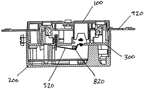
Fig. lA shows a GFCI device 1 that is constructed in accordance with the
principles of
the invention. The GFCI device can have a top housing cover 100 that is
constructed of a size
and shape that is consistent with industry standards for an electrical outlet.
Preferably, the device
2 0 includes two sets of receptacle openings for receiving standard plugs. A
test/reset aperture can
be located along a mid-line of the top housing cover 100 and include a test
button 801 and reset
button 802 located therein. A light aperture 108 can also be located on the
mid-line of the top
ua018/J619.1
CA 02298831 2000-02-15
housing cover 100 to enclose a light for indicating whether the GFCI device
has been tripped due
to either a ground fault detection or a test of the device. The light can also
indicate whether the
GFCI device has been correctly wired.
Top and bottom angled indicia surfaces 101 can be provided on either side of
the mid-line
and include indicia thereon. The indicia can include numerals, letters,
symbols or other markings
that can be viewed from the exterior of the GFCI device and which preferably
provide an
instructional message to a viewer. In the embodiment depicted in Fig. lA, the
indicia comprise
the terms "test" and "reset" to instruct a viewer of the function of the
buttons located adjacent the
indicia surfaces. The angled indicia surfaces are preferably sloped at a 45
° angle with respect to
the substantially planar face surface 107 of the top housing cover 100 so that
the indicia can be
read from above and below the GFCI device. Accordingly, a user can read the
indicia on the
angled indicia surfaces 101 regardless of the orientation of the GFCI device
when installed.
Furthermore, it should be appreciated that this preferred configuration de-
emphasizes the visual
appearance of indica on the top indicia surface and emphasizes indicia located
on the bottom
indicia surface when viewed from above, e.g., when the device is installed in
a wall.
A mounting strap 920 extends from either side of the top housing cover 100 for
attaching
the GFCI device to a wall box. Indents 103 can be provided on either side of
the top housing
cover 100 to facilitate connection to electrical wires.
Fig. 1B shows an isometric view of the bottom housing cover 200 which is
attached to
2 0 the top housing cover 100 via screws inserted through the connection holes
201 in the bottom
housing 200. Neutral connection holes 202 and hot connection holes 203 are
located in the
bottom housing cover 200 to provide an alternate connection for input wires
onto the GFCI
NA018/3619.1 - 1 O -
CA 02298831 2000-02-15
circuit. In addition, neutral connection holes 204 and hot connection holes
205 are located on the
bottom housing cover 200 to provide an alternate attachment structure for
output wires leading
from the GFCI circuit. A wide pathway 20b can be located at one end of the
periphery of the
bottom housing cover 200 to facilitate attachment of a U-shaped wire connector
to the grounding
screw of the GFCI device. Indents 208 may also be provided on the bottom
housing cover 200
and aligned with the indents 103 of the top housing cover 100 to provide
clearance for U-shaped
wire attachment structures for input and output wires.
As shown in Fig. 2, the top housing cover 100 and the bottom housing cover 200
encase
the GFCI components and circuitry including a middle housing 300 and circuit
board 950
therebetween. The middle housing 300 is located above the circuit board 950
and adjacent the
top housing cover 100. The circuit board 950 rests adjacent the bottom wall of
the bottom
housing cover 200. The middle housing 300 can be a one piece molded structure
that has a
plurality of ribs thereon to locate and stabilize the GFCI circuit components.
A mounting strap
920 can be sandwiched between the top housing cover 100 and the middle housing
300 and
extend from either end of the GFCI device so that the GFCI device can be
mounted to a
conventional wall box.
The GFCI circuitry as shown in Fig. 2 includes a transformer device for
detecting a
ground fault, a solenoid trip device for causing both current pathways of the
GFCI device to
open, and a test/reset structure for periodically testing the GFCI device and
for resetting the
2 0 GFCI device after it has been either tested or tripped.
Figures 3A and 3B depict an exploded view and an isometric view, respectively,
of the
electronic components 951 and other various components that are located on the
circuit board
W 018/3619.1 - 1 1 -
CA 02298831 2004-03-08
950 of the GFCI device. The electronic components 951 include resistors,
capacitors:and other
well known electronic circuit components for comprising a GFCI circuit. The
eleetmnie
components 951 can be attached to the circuit board 950 via any well known
attachment method,
e.g., by soldering. The circuit board 950 can include clip apertures 952 and
pivot apertures 953
for attaching the transformer boat 400 and the solenoid bobbin 700 quickly and
easily with
lock/alignment pins and clips located on the base of each of the transformer
boat 400 and
solenoid bobbin 700:
The test light 901 can be raised from the circuit board 950 by the
standoff~900. The,
_ standoff 900 is preferably a two=piece.snap together structure as described
in applicant's
U.S. Patent No. 6,349,908, entitled "Standoff Assembly and Method for
Supporting an Electrical
Component", which issued February 26, ZUU2.
Elements of the, current path can be attached to the circuit board at a hot
attachment point
and a neutral attachment point. ~ Specifically; hot contact aim 520 and hot
input terminal 550 can
be soldered together and to the circuit board 950 at a location underneath the
transformer boat
400. Likewise, the neutral contact anm 620 and neutral input terminal 650 can
be soldered
together and to the circuit board 950 at a location underneath the transformer
boat 400 and
adjacent to the hot attachment point. Accordingly, electrical power can be
suppliod to the
electronic components 951 and all other electronic devices located on the
circuit board 950 via
the hot input terminal 550 and neutral input terminal 650.
As.shown in Fig. 4, the top housing cover 100 can include tapped or self
tapping
attachment holes 102 located at the corners of the top housing cover 100 for
screw connection to
the bottom housing 200. Contact cavities 104 are shown located in the central
portion of the top
housing cover 100 for sealing and protecting the area in which contacts are
located,in the hot and
-12-
CA 02298831 2000-02-15
neutral current paths. Test reset aperture 105 can be configured as a long,
narrow rectangular
opening in the central portion of the top housing cover 100. The tesdreset
aperture 105 permits
the test button 801 and reset button 802 to be contactable from outside of the
top housing cover
100.
5. A reset pin guide 106 can be formed as part of the back surface of the top
housing cover
100 to stabilize and guide the motion of the reset button 802 and shaft 804 in
a linear path when
they are actuated.
Light aperture 108 can be located adjacent the test/reset aperture 105 for
convenient
viewing. The test light 901 is aided by the standoff 900 to extend from the
circuit board 950 and
l0 into the light aperture 108.
Ground hole 110 and slots 109 are shown arranged in the North American
standard
configuration for household electrical outlets. Although not shown, other
configurations for the
ground hole 110 and slots 109 are well known for complying with other types of
electrical plugs
as appropriate in various area of the world and for various applications.
1 ~~ As shown in Fig. 5, the bottom housing 200 can be a unitary one piece
structure that is
generally rectangular in shape and includes connection holes 201 located at
each corner. The
connection holes 201-are in alignment with the attachment holes 102 in the top
housing cover
100 for connecting the top and bottom housing covers 100, 200 by a screw, nail
or other
fastening device.
2 o The bottom housing 200 of the GFCI device can be configured with several
different
input and output connection options. In particular, indents 208 can be
provided at the sides of
the bottom housing 200 to facilitate connection between a U-shaped connector
on an input wire
NA018/J619.1 - 1 ~ -
CA 02298831 2000-02-15
to a screw/face terminal connection 961 provided on one of the current
pathways of the GFCI
circuitry. In addition, bottom housing 200 can be provided with neutral input
connection holes
202, hot input connection holes 203, neutral output connection holes 204 and
hot output
connection holes 205. The connection holes 202-205 permit bare electrical
lines access to the
GFCI circuity. Specifically, a bare wire inserted into one of the connection
holes 202-205 can be
guided to an area between a connection face plate 963 and its associated wire
connector surface,
e.g., wire connector 508,551,608 or 651. After insertion, the bare wire can be
clamped into
connection with one of the current pathways by turning a screw of a screw/face
terminal to cause
the connection face plate 936 to close onto and clamp the bare wire between
the connection face
plate 963 and a wire connector 508,551,608 or 651. The connection face plate
963 can include
horizontal grooves therein to prevent a bare wire connected thereto from
slipping out of
connection with the connection face plate 963. A bare wire connection can be
made alternatively
or in addition to the connection of a U-shaped wire terminal to the screw/face
terminals 961
located at the sides of GFCI housing.
The screw/face terminals 961 can be situated in the bottom housing 200 such
that they
can be connected to either a U-shaped connector on the end of a wire at indent
208 or to a bare
wire that is inserted into one of the connection holes 202-205. The U-shaped
wire terminal can
be clamped between the screw head of the screw/face terminal 961 and the outer
surface of one
of the wire connectors 508,551,608 or 651.
2 Ci Figures 6A and 6B show the hot and neutral current pathway structures,
respectively, of
the GFCI device. Figure 6A depicts the various structures that make up the hot
current pathway
for the GFCI device and shows their relative position as assembled. The hot
current pathway can
11A018/3619.1 - 14 -
CA 02298831 2000-02-15
consist of a hot input terminal 550, a hot contact arm 520 two contacts 501
and 521 and a hot
output terminal 500. The hot input terminal 550 can be configured to be
attachable to an
electrical wire for receiving positive (hot) current into the current pathway.
The hot input
terminal 550 can be attached to the hot contact arm 520 by soldering or the
like. Additionally,
both the hot input terminal S50 and hot contact arm 520 can be anchored to the
circuit board 950
by the same solder connection that connects the two structures together. The
hot contact arm 520
can be figured to include a contact stem 522 that extends through the center
of a transformer coil
408 located in the transformer boat 400 when assembled. Current passing
through the contact
stem 522 is compared by the transformer coil 408 to the current returning
through a similar
1 o contact stem 622 located on the neutral contact arm 620. In accordance
with the laws of physics,
an electrical current will be induced in the transformer coil 408 when there
is a differential
between the current flows in contact stems 522 and 622. Once a predetermined
current is
induced in the transformer coil 408, a ground fault will be indicated by the
GFCI device and the
current paths will be opened as explained later.
1 ~~ The hot contact arm 520 can be reparably connected to the hot output
terminal 500 via a
pair of contacts SO1, X21. Contact 521 can be located on a cantilevered arm
portion the hot
contact arm 520 and contact SO1 can be located on a stationary arm of the hot
output terminal
500. Accordingly, a downward force applied to the cantilevered arm portion
will force the
contact 521 out of contact with the contact SO1 located on the hot output
terminal 500 to open the
2 0 hot current pathway. The hot output terminal 500 can be reparably
connected to the hot contact
arm 520 as explained above and can include two conventional spring type
electrical receptacle
contacts 504 and a wire connector 508. The wire connector 508 and receptacle
contacts 504 can
bIA0lB/J619.1 - 15 -
CA 02298831 2000-02-15
be connected to an outside circuit, e.g., to an appliance, other electrical
device or other electrical
receptacle.
As shown in Figure 6B, the neutral current pathway structure can consist of a
neutral
input terminal 650, a neutral contact arm 620, a pair of contacts 601, 621 and
a neutral output
terminal 600. The neutral input terminal 650 can be attached to an electrical
wire at one end and
soldered to the circuit board 950 and the neutral contact arm 620 at the
opposite end. The neutral
contact arm 620 includes a contact stem 622 that can be positioned adjacent
the contact stem 522
of the hot contact arm 550 and through the transformer coil 408 to allow
ground fault detection
as explained above. Contact 621 can be located at a distal end of a
cantilevered arm portion of
the contact arm 620 and contact 601 can be located on a stationary arm of the
neutral output
terminal. The cantilevered arm portion is configured such that contact 621
will separate from
contact 601 when a downward force is applied to the cantilevered arm portion
of the contact arm
620. Accordingly, the neutral current pathway can be opened by a linear
downward force
applied to the cantilevered arm portion. In addition, the hot contact arm 520
and neutral contact
arm 620 can be located adjacent each other when assembled into the GFCI
housing such that a
single structure, e.g., latch block assembly 810, can provide the downward
linear force necessary
to simultaneously open both the hot and neutral current pathways. The neutral
output terminal
600 can be reparably connected to the neutral contact arm 620 at contact point
601 as explained
above. The neutral output terminal 600 also includes two conventional spring
type electrical
2 0 receptacle contacts 604 and a wire connector 608 for connecting a neutral
electrical conductor
between the GFCI device and an appliance or other electrical device or
receptacle.
W1018/3619.1 - 1 6 -
CA 02298831 2000-02-15
As shown in Figs. 7A-7D the middle housing 300 can be molded from a unitary
piece of
plastic and be configured to fit within and be clamped between the top housing
cover 100 and
bottom housing cover 200. The middle housing 300 is preferably a different
color as compared
with the top housing 100 and bottom housing 200 to more clearly indicate where
electrical wires
can be connected to the GFCI device. For example, the middle housing 300 is
preferably blue
while the top housing 100 and bottom housing 200 are preferably white and
grey, respectively.
A pair of contact arm through holes 306 can be provided iri the central area
of the middle housing
300 so that the far end of the cantilevered portions of the hot and neutral
contact arms 520 and
620, can pass through the middle housing 300 allowing each pair of contacts
501, 521 and 601,
1 C~ 621 to contact each other. Thus, the middle housing 300 protects the
circuit board 950 from any
sparking that may occur between pairs of contacts SO1, 521 and 601, 621 when
they are
separated from or contacted to each other.
The top portion of the middle housing 300 can be configured to align the hot
output
terminal 500 and the neutral output terminal 600 and to electrically separate
both of these
structures from each other and from the components located on the circuit
board. The hot output
terminal 500 and neutral output terminal 600 can be located between the top
housing cover 100
and the middle housing 300 such that a conventional plug will have access to
the hot output
terminal 500 and neutral output terminal 600 when inserted through slots 109
in the top housing
cover 100.
2 0 A test resistor through hole 304 in the central portion of the middle
housing allows a test
resistor to pass therethrough. As will be explained in more detail later, the
test resistor allows the
GFCI device to be tested by simulating a ground fault by diverting current
through the test
IdA018/J619.1 I 7
CA 02298831 2000-02-15
resistor from the hot output terminal and eventually to the neutral input
terminal through the
circuit board 950. A light standoff through hole 302 can be located in the
middle housing 300 to
support the standoff 900 as it extends from the circuit board to the top
housing cover 100.
Likewise, a reset shaft through hole 320 can be placed in a central area of
the middle housing 300
to permit the reset shaft 804 to pass therethrough and to guide the reset
shaft 804 along a linear
path. In addition, the reset shaft through hole 320 includes a countersunk
portion on the bottom
side of the middle housing, as shown in Fig. 7C and 7D, that allows a latch
block 820 and latch
block actuation spring 812 to reside therein. Accordingly, the reset shaft
through hole struchue
guides the latch block 820 along the same linear path as taken by the reset
shaft when moved.
A hot output terminal throughway 316 and a neutral output terminal throughway
318 can
be located at either side of the middle housing to allow the U-shaped wire
connectors 508 and
608 to pass through the middle housing 300 and be exposed at either side of
the GFCI device for
connection to electrical wires. A test button guideway 322 can be located in
the top portion of
the middle housing 300 for guiding the test button 801 along a linear path and
into contact with
1!~ the test switch arm 502 of the hot output terminal 500. The test button
801 can be located above
and guided within the top portion of the middle housing 300 above the test
resistor through hole
304.
The bottom portion of the middle housing 300 can include alignment holes 324
that mate
with alignment posts 419 located on the transformer boat 400. Alignment
between all of the
2 0 components of the GFCI device is important to ensure that the hot and
neutral contacts 501,521
and 601, 621, respectively, remain in contact with each other when the GFCI
device is in its
"reset position" and to ensure that the contacts will be out of contact with
each other when the
LdApl9/J619.1 - 1 g -
CA 02298831 2000-02-15
GFCI device is in its "tripped position." A transformer boat indent 308 and a
solenoid bobbin
indent 314 can be provided in the bottom portion of the middle housing 300 to
secure and align
the transformer boat 400 and solenoid bobbin 700. A hot contact arm indent 310
and a neutral
contact arm indent 312 can be separated from each other by a separation wall
326 to provide
alignment structures for the hot and neutral contact arms 520 and 620,
respectively, to reside in.
The separation wall 326 also electrically insulates the contact arms 520 and
620 from each other.
Screw/face supports 327 can extend from the bottom of the middle housing 300
and into
the central opening of the U-shaped wire connectors 551 and 651 located on the
hot input
terminal 550 and neutral input terminal 650, respectively. The screw/face
supports 327 serve to
retain the screw/face terminals 961 in a general area and provide support when
the screw/face
terminals 961 are used to lock down an electrical wire.
As shown in Figs. 8A-8D, the hot output terminal S00 and neutral output
terminal 600
can each be constructed as a one-piece structure that is made from an
electrically conductive
material such as brass. The hot output terminal S00 can include two receptacle
contacts 504 that
are disposed adjacent slots 109 in the top cover housing 100 when assembled.
As shown in Fig.
8A, the receptacle contacts 504 are standard spring receptacle contacts that
are adapted to receive
a standard 120V North American plug. However, different receptacle contacts
can be used
depending on the location and application of the GFCI device. U-shaped wire
connector 508
extends from one end of the hot output terminal such that, when assembled, it
will be located at
2 0 and accessible from the side of the GFCI device for attachment to an
electrical wire. A contact
SO1 configured for connection to a contact 521 on the hot contact arm 520 can
be located on an
arm that extends laterally from the hot output terminal 500. The extended arm
portion of the hot
11n010/~619.1 - 1 ~ -
CA 02298831 2000-02-15
output terminal 500 is relatively short and rigid such that the attached
contact 501 remains
stationary with respect to the hot output terminal 500 and the middle housing
300 in which the
hot output terminal 500 resides.
A test switch arm 502 can be provided as an integral lateral extension from
the hot output
terminal 500. The test switch arm 502 can be configured to reside over the
test resistor through
hole 304 and under the test button 801 when assembled in the GFCI device. The
test switch arm
502 is also of such a length and rigidity that depression of the test button
801 from outside the
GFCI device will cause the test button 801 to contact and bend the test switch
arm 502 into
contact with a test resistor located in the test resistor through hole 304 of
the middle housing 300.
1 C~ Current that flows from the hot output terminal 500 through the test
switch arm 502 to the test
resistor will (if the GFCI device is operating correctly) cause the GFCI
device to indicate a
ground fault has occurred and subsequently trip the GFCI device to open the
current pathways.
The neutral output terminal 600 can also include two receptacle contacts 604
constructed
in a similar fashion as are receptacle contacts 504 of the hot output terminal
500. A wire
1 > connector 608 can also be provided on the neutral output terminal 600. A
contact 601 can be
provided on a relatively short and rigid extension arm on the neutral output
terminal 600 for
connection to a contact 621 located on the neutral contact arm 620.
As shown in Figs. 9A and 9B, hot contact arm 520 and neutral contact arm 620
can each
be configured as a unitary structure that is basically a mirror image of each
other. The hot
2 o contact arm 520 can include a contact stem 522 that is designed to extend
through the center of
transformer coils 408 in the transformer boat 400. A distal end of the contact
stem 522 can be
soldered, welded or otherwise electrically connected to both the circuit board
950 and connecting
h1A018/3619.1 - 2~ -
CA 02298831 2000-02-15
tab 552 of the hot input terminal 550. The opposite end of the contact stem
522 includes a stop
tab 526 that extends from a side of the contact stem 522 for abutting against
the transformer boat
400. The stop tab 526 ensures the correct insertion depth of the contact stem
522 into the circuit
board and correctly aligns the hot contact arm 520 with the transformer boat
400 and GFCI
circuitry. The hot contact arm 520 includes a series of bends at its middle
portion to navigate
around the transformer boat structure. Another stop tab 526 and an alignment
post 524 can
extend into transformer boat 400 and are located in the middle portion of the
contact arm 520 to
align the contact arm 520 within the GFCI device. A cantilevered arm portion
extends from the
middle portion and has a through hole at its distal end for connection to
contact 521. When
assembled in the GFCI device, the cantilevered arm portion extends through the
middle housing
such that contact 521 is normally in contact with contact 501 of the hot
output terminal 500. In
addition, the cantilevered arm portion is of such a length and dimension that
it can be forcibly
flexed about a position adjacent to the alignment post 524. Accordingly,
contact 521 can be in
contact with contact 501 when in the reset position and forcibly flexed away
from and out of
1 S contact with contact SO1 when in the tripped position. The stop tabs 526
and alignment tab 524
ensure that the contact arm 520 is positioned correctly so that the contacts
501 and 521 will be in
contact and out of contact in their reset and tripped positions, respectively.
In particular,
alignment tab 524 is designed to extend into an alignment tab receptacle 422
in the transformer
boat 400 at a depth set by stop tab 526 to secure the position of the contact
arm 520 with respect
2 0 to the transformer boat 400. ~In addition, the alignment tab 524 and stop
tab 526 create an anchor
point from which the cantilevered arm portion can flex.
t~A018/J619.1 - 2 1 -
CA 02298831 2000-02-15
The neutral contact arm 620 can include similar structures that perform
relatively
identical functions as compared to the hot contact arm 520. Moreover, neutral
contact arm 620
can include stop tabs 626 and alignment tab 624 for alignment with the
transformer boat 400 and
for providing an anchor point for a cantilevered arm portion of the neutral
contact arm 620.
Contact stem 622 is designed to extend through the transformer boat 400
adjacent to the contact
stem 522 of the hot contact arm 520 and be similarly electrically attached to
both the circuit
board 950 and the corresponding neutral input terminal 650 at a distal end of
the contact stem
622. A contact 621 can be located at a distal end of the cantilevered portion
of the neutral
contact arm for connection to contact 601 of the neutral output terminal when
in the reset
position, and for forcible separation from the contact 601 when in the tripped
position.
As shown in Figs. l0A-IOD, the neutral input terminal 650 and hot input
terminal 550
can each be a one-piece unitary structure made from electrically conductive
material. The
neutral input terminal 650 can be an approximate mirror image of the hot input
terminal S50 and
include a U-shaped wire connector 651, a connection tab 652 and a pair of
mounting tabs 654.
1 ~~ The mounting tabs 654 and connection tab 652 can be assembled onto the
circuit board 950 such
that they extend through and are soldered onto the circuit board 950.
Connection tab 652 can
also be soldered to the contact stem 622 of the neutral contact arm 620 such
that electrical current
can pass between the neutral contact arm 620 and neutral input terminal 650.
The U-shaped wire
connector 651 can be arranged at an approximate 90 degree angle with respect
to the base of the
2 0 neutral input terminal 650 so~ that, when installed, the wire connector
651 is located at and
accessible from a side of the GFCI device. The location of the wire connector
651 provides easy
connection to an electrical wire via the screw/face terminal 961.
t,INO1Bi3619.1 - 22 -
CA 02298831 2000-02-15
As stated above, the hot input terminal 550 can be constructed as an almost
identical
mirror image of the neutral input terminal 650. Specifically, the hot input
terminal S50 can
include a U-shaped wire connector 551 that is configured at a 90 degree angle
with respect to a
base portion of the hot input terminal 550. Mounting tabs 554 and connecting
tab 552 can
S extend from the bottom of the base portion for electrical connection to the
circuit board 950 via
soldering or other known permanent electrical connection. The connection tab
552 can also be
electrically connected to the contact stem 522 of the hot contact arm to
create a current pathway
therebetween.
As shown in Fig. 11, test button 801 can be formed of a single-piece non-
conductive
1 Ci material, for example, plastic. The test button 801 is design to have a
push surface (as shown in
Fig. lA) that extends from the test/reset aperture 105 in the top housing
cover 100. The test
button 801 can be depressed by a user to cause the GFCI circuitry to simulate
a ground fault
detection, thereby testing whether the GFCI device is working properly. Stop
flanges 808 can be
located at either side of the test button 801 to abut a side of the test/reset
aperture 105 and
1 p prevent the test button 801 from being removed from the top housing cover
100. A test switch
arm contact surface 803 can be located below the push surface of the test
button 801 and at the
end of an extension supported by guide rib 809. The contact surface 803 can be
designed to
contact the test switch arm 502 of the hot contact arm such that the
resiliency of the test switch
arm 502 keeps the test button in a protruded state from the test/reset
aperture 105 in the top
2 0 housing cover 100. In addition, when the test button 801 is depressed, the
contact surface 803
can be situated such that it forces the test switch arm 502 to flex downward
and contact a test
resistor located in the test resistor throughway 304 to simulate a ground
fault and test whether the
HA018/~619.1 - 23 -
CA 02298831 2000-02-15
GFCI device is operating properly. The test button 801 can be guided along a
linear path during
depression by guide rib 809 acting in conjunction with the test button
guideway 322 in the
middle housing 300.
As shown in Figs. 12A, 12B and 13, latch block assembly 810 can include three
major
components: a latch block 820, a latch 840, and a latch charging spring 830.
The latch block
assembly 810 works in conjunction with other elements of the GFCI device to
perform various
functions, including retaining the reset shaft 804 in its "reset" position,
and, causing the contacts
501, 521 and contacts 601; 621 to decouple from each other to open the GFCI
circuitry when a
ground fault is detected. The latch block 820 can be T-shaped with arms 821
that extend from
10~ opposite sides of a main body portion 826 and a shield tube 822 that
extends from the main body
portion and is located between the arms 821. A through hole 824 extends
through the shield tube
822 to the opposite side of the main body portion 826. Latch guides 823 can be
formed at the
bottom of the latch block 820 and on either side of the through hole 824 for
guiding the latch 840
along the bottom surface of the latch block 820. When assembled, an opening in
the latch 840
1 > corresponds with the through hole 824 of the latch block 820 to permit the
reset shaft 804 to pass
through both structures. The shield tube 822 provides protection from the
possibility of any
arcing to the reset shaft 804 and/or other structures during operation.
Latch 840 can be slidably located in the latch guides 823 and include a latch
edge 843 for
locking into latch groove 805 of the reset shaft 804 when in the reset
position. The latch edge
2 ~7 843 can be biased towards the reset shaft 804 by a latch charging spring
830 connected between
the main body portion 826 of the latch block 820 and a striking plate 841 of
the latch 840. The
charging spring 830 can be aligned to the striking plate 841 by a spring catch
tab 844 located on
uaoieiasi9. i - 24 -
CA 02298831 2000-02-15
an inside face of the striking plate 841. A spring guide pin 825 preferably
extends from the main
body portion 826 of the latch block towards the striking plate 841 to guide
the charging spring
830 and maintain its alignment between the latch block 820 and latch 840. The
latch 840 can
include a pair of catch tabs 842 located on either side of an end of the latch
840 opposite the
striking plate 841. Catch tabs 842 are bent slightly downward such that they
can pass through
latch guides 823 during assembly and then spring outward after assembly to
prevent removal of
the latch 840 as a result of contact between catch tabs 842 and either the
latch block 820 or the
latch guides 823.
As will be discussed in detail later, the latch block assembly 810 is slidably
mounted on
the reset shaft 804 such that a latch block actuation spring 812 (as shown in
Fig. 18) can cause
the latch block assembly to slide down the reset shaft to disengage contacts
501, 521 and 601,
621 and thus open the GFCI circuitry current pathways when a ground fault is
detected.
As shown in Figs. 14A-14B, solenoid bobbin 700 can include a solenoid frame
733,
solenoid winding 703 and solenoid armature 712 {as shown in Fig. 2). Solenoid
winding 703 can
be wound on a spool 731 located between solenoid end plates 704 and 705. The
solenoid
functions to trip the latch 840 of the latch block assembly 810 when a ground
fault is detected
such that the latch 840 is released from the latch groove 805 in the reset
shaft 804. Once the
latch 840 releases the reset shaft 804, the latch block actuation spring 812
forces the latch block
assembly 810 to slide along the reset shaft 804 and eventually contact the
cantilevered portion of
2 t) the hot and neutral contact aims 520 and 620. Accordingly, contacts SO1,
521 and 601, 621 are
caused to separate from each other, and the current pathways are thus opened
by the downward
sliding motion of the latch block assembly 810 when a ground fault is
detected.
W1010/3619.1 - 2~ -
CA 02298831 2000-02-15
The solenoid bobbin 700 can include a one-piece solenoid frame 733 that is
preferably
made from a plastic material. A spool 731 with end-plates 704 and 705
bordering the spool 731
can be located at one end of the frame 733. A rectangular window portion 732
can be located at
the opposite end of the solenoid frame 733. The rectangular window 732 can
include a reset
shaft throughway 710 for guiding the reset shaft 804 when it is depressed to
reset the latch block
assembly 810 to its reset position. A component support 708 preferably extends
from a side of
the rectangular window portion 732 for providing support for and protecting an
electrical
component 951 extending from the circuit board 950. A shelf 706 can be located
at a distal end
of the rectangular window portion 732. Shelf 706 is designed to mate with a
support arm 404
located on the transformer boat 400 and cooperate therewith to provide added
support to the
circuit board 950 ancY transformer boat 400. Specifically, shelf 706 resides
under and is in
overlapping contact with the support arm 404 such that when the circuit board
950 is flexed or
bent at a location between the transformer boat 400 and solenoid bobbin 700,
the shelf 706 and
support arm 400 prevent substantial movement of the circuit board 950 in the
flexing or bending
directions. In addition, contact between support arm 404 and shelf 706
provides reliable support
to test resistor throughway 402 to ensure correct positioning of the
throughway 402 and test
resistor.
The solenoid bobbin 700 can be attached to the circuit board by a pivot and
clip
mechanism in which an alignment extrusion 720 that extends fro the base of the
shelf 706 is
2 C~ placed within a pivot aperture 953 in the circuit board 950. The solenoid
bobbin 700 can then be
pivoted downward about the alignment extrusion 720 to lock a snap-in lock hook
718 into a clip
aperture 952 in the circuit board 950. The snap-in lock hook 718 can be
located on the end of the
Wv010/J619.1 - 26 -
CA 02298831 2000-02-15
rectangular window portion 732 opposite the alignment extrusion 720. In
addition, the snap-in
lock hook 718 can be constructed to flex upon entry into the clip aperture 952
and then return to
its original configuration once the hook portion of the snap-in lock hook 718
has passed through
the clip aperture 952. Thus, the snap-in lock hook 718 permanently attaches
the solenoid bobbin
700 in place on the circuit board 950.
The spool portion 731 of the solenoid bobbin 700 includes a wire relief slot
709 for
protecting the initial starting portion of wire of the solenoid winding from
being damaged by the
winding process. An armature throughway 719 can extend through the spool 731
and open into
the rectangular window portion 732. The armature throughway 719 preferably
includes
guidancelfriction reducing ribs 730 that guide and facilitate easy movement of
a solenoid
armature 712 located within the armature throughway 719. The armature 712 is
preferably a
metallic cylinder shaped structure that includes an armature tip 713 at one
end. The armature tip
713 can be configured to contact the striking plate 841 of the latch 840 when
the armature 712 is
at its fully extended position relative to the armature throughway 719.
1 , First and second terminal holes 707 can be located on the bottom corners
of end plate 705
for connection to the circuit board 950. The first and second end of the wire
that forms the
solenoid winding 703 can be attached to first and second terminal pins that
extend into terminal
holes 707 from the circuit board to supply electrical power from the circuit
board 950 to the
solenoid. Upon receiving power from the circuit board, the magnetic field
created by solenoid
2 ~0 winding 703 forces the solenoid armature 712 into contact with the
striking plate 841 of the latch
840 to move the latch against the bias of the latch charging spring 830.
HA018/3619.1 27
CA 02298831 2000-02-15
As shown in Figs. 15A and 15B, a solenoid bracket '102 can be a single-piece
structure
that includes two arms extending from a base to form a U-shaped bracket. An
alignment dimple
721 can be provided on the inside surface of one of said arms to align the
bracket within the
armature throughway 719 of the solenoid frame 733. A throughway is provided at
the center of
the dimple to permit the armature tip 713 to pass through when actuated and
contact the striking
plate 841. An armature throughway 714 can extend through the other of said
arms of the
solenoid bracket 702 to permit the armature 712 to pass therethrough. The
armature throughway
714 can include a key notch 716 that rides over and locks onto a locking ramp
711 in the
solenoid end plate 705.
As showing in Figs. 16A and 16B, the transformer boat 400 can be a relatively
cylindrical
object having a plurality of arms 418 extending from the sides of the
cylindrical structure. The
transformer boat 400 can include a pair of transformer coils 408 that are
separated by a first
insulating washer 407 and covered by a second identical insulating washer 407.
Insulating
washers 407 can be provided with indents around its inner diameter that allow
the washer to
1 ~~ easily flex over and lock onto the inner cylindrical portion 405. A
contact stem throughway 406
and throughway separator 416 can be provided through the center of the inner
cylindrical portion
405 for allowing contact stems 522 and 622 to pass on either side of
throughway separator 416.
The throughway separator 416 can include a pair of ridges that run through the
center of the
contact arm stem throughway 406 and ensure that the hot and neutral contact
stems 522 and 622
2 n do not contact each other, arc between each other, or otherwise short each
other out. In a
preferred embodiment, the pair of ridges can be formed as a single thick
ridge.
Wv018/9619.1 - 2g -
CA 02298831 2000-02-15
An outer cylindrical portion 409 can encase the transformer coils 408 and
include a
plurality of arms 418 extending therefrom to stabilize the transformer boat
400 by spreading out
the points of attachment with the circuit board 950. In addition, the
plurality of arms 418 create
an enclosure around the screw/face terminals 961 to keep the connection face
plates 963 from
turning and contacting other internal parts of the GFCI device. An alignment
post 419 can be
integrally formed on the top side of each arm 418 for extension into
corresponding alignment
holes 324 in the middle housing 300 to ensure alignment of all GFCI
components. In addition,
contact arm alignment receptacles 422 can extend along a side of the outer
cylindrical portion
409 so that alignment tabs 524 and 624 of the hot and neutral contact arms 520
and 620,
respectively, can be inserted therein. The specific configuration of the
alignment receptacles 422
ensures the critical alignment of the contact arms 520 and 620 with the hot
and neutral output
terminals 500 and 600.
As discussed previously with respect to the solenoid bobbin 700, a support arm
404 can
extend from the outer cylindrical portion 409 of the transformer boat 400 to
contact with the
1 ~> shelf 706 of the solenoid bobbin. The support arm 404 and shelf 706
cooperatively strengthen
the flexural stability of the circuit board 950. In addition, support arm 404
can be provided with
a test resistor throughway 402 that is configured to encapsulate and stabilize
the top of a resistor
while allowing a resistor lead to extend through the throughway 402 and be
bent over the
structure forming the throughway 402. The shelf 706 fiuther secures the
correct positioning of
2 c) the test resistor throughway 402 when the test button is depressed.
Accordingly, the test resistor
lead will be precisely located within the GFCI device and will ensure the
working accuracy of
W018/3619.1 - 29 -
CA 02298831 2000-02-15
the test button. Specifically, test switch arm 502 will be able to repeatedly
contact the lead of the
test resistor with a high degree of certainty.
The base of the transformer boat 400 can include a lock/alignment pin 412,
lock clip 414
and a set of terminal pins 420. The lock alignment/pin extends from the base
of the transformer
boat and fits into a pivot aperture 953 in the circuit board 950. Lock clip
414 also extends from
the base of the transformer boat 400 and, during assembly, is flexed into a
clip aperture 952 in
the circuit board to lock the transformer boat 400 securely to the circuit
board 950. Terminal
pins 420 also protrude from an extension of the base of the transformer boat
400 and are
electrically connected to the circuit board 950 by soldering or other known
attachment structure.
Terminal pins 420 are also electrically connected to the transformed coils 408
and communicate
to the GFCI circuitry any current changes in the hot and neutral contact arm
stems 522 and 622
as sensed by the coils 408.
As shown in Fig. 17, circuit desensitizing switch 850 can be configured as a
one-piece
structure that has two arms 852 and a contact extension 853. The arm 852 and
contact extension
853 extend from a base 854 of the desensitizing switch 850. A tab 855 can be
soldered to the
circuit board 950 to keep the contact extension 853 centered over a
desensitizing contact 851
located on the circuit board 950. When assembled, the base 854 can be
electrically connected to
the circuit board 950 by a tab 855 that extends from a window of the base
portion 854. Two side
wings 856 can extend from either side of the base 854 for securing the switch
850 between the
2 0 solenoid bobbin 700 and the circuit board 950. The arms 852 and contact
853 can be
cantilevered upwards and away from the base portion 854 such that they are
resiliently
positioned over the circuit board. Specifically, the cantilevered
configuration permits contact
NA018/3619.1 - 30 -
CA 02298831 2000-02-15
853 to be resiliently situated above desensitizing contact 851 (shown in Fig.
18A) located on
circuit board 950. Contact 853 and arms 852 are also located immediately
underneath and along
a linear path of the latch block assembly 810. Accordingly, contact 853 can be
depressed by the
action of side wall ends 857 pressing on arms 852 when latch block assembly
810 moves into its
fully tripped position to cause contact 853 to connect with desensitizing
contact 851 and
deactivate the GFCI device. Thus, the GFCI device can be prevented from
sensing further
ground faults or activations of the test button until it is reset by the
test/reset switch 800.
The operation of the testJreset switch 800 will be explained with reference to
the
sequential skeletal drawings of Figs. 18A-D. Figs. 18A and 18B show the GFCI
device in its
1 C~ "tripped" position after the device has either sensed a ground fault or
the test button has been
depressed, and the device has not yet been reset.
In the "reset" position as shown in Figs. 18C and 18D, the latch block
assembly 810 is
retained adjacent the middle housing 300 and above and out of contact with the
contact arms 520
and 620. Thus, the hot and neutral current pathways of the GFCI device are
closed and permit
1 p current to flow to a circuit connected to the GFCI device. Moreover, the
elasticity of the
cantilevered portions of contact arms 520 and 620 keep the contacts 521 and
621 in electrical
connection with contacts 501 and 601 of the hot and neutral output terminal,
respectively, to
keep the hot and neutral pathways closed when the GFCI device is in its
"reset" position..
The latch block assembly 810 is retained in the "reset" position by latch 840
that is
2 0 locked into latch groove 805'of the reset shaft 804. The locked connection
between the latch 840
and the latch groove 805 keeps both the reset spring 811 and the latch block
actuation spring 812
in a compressed state. In the "reset" position, the reset button 802 can be
slightly spaced apart
W1018/3619.t - 3 1 -
CA 02298831 2000-02-15
from the top housing cover 100. This spacing results from compressive forces
of reset spring
811 forcing the shield tube 822 of the latch block 820 into contact with the
middle housing 300.
The position at which the reset shaft 804 is locked by latch 840 to the latch
block assembly 820
prevents the reset shaft 804 and reset button 802 from extending to the top
housing cover 100.
In operation, the latch block assembly 810 can be moved from its "reset"
position to its
"tripped" position by the force of latch block actuation spring 812 when the
latch 840 is unlocked
from the reset shaft 804. Latch 840 can be unlocked from the reset shaft by
the solenoid
armature which, when actuated, contacts the striking plate 841 of the latch
840 to cause the latch
840 to slide along the base of the latch block 820 against the compressive
force of the latch
1 o charging spring 830. As the latch 840 slides along the base of the latch
block 820, latch edge
843 is withdrawn from the latch groove 805 in the reset shaft 804. Thus, the
compressive force
of the reset spring 811 causes the reset shaft 804 and reset button 802 to
move upwards and into
contact with the top housing cover 100, while the compressive force of the
latch block actuation
spring 812 simultaneously causes the latch block assembly 810 to slide
linearly down the reset
shaft 804. In addition, the linear downward movement of the latch block
assembly 810 causes
the arms 821 of the latch block 820 to contact the cantilevered arm portions
of the hot and neutral
contact arms 520 and 620, respectively. The contacts 501, 521 and 601, 621 can
thus be
separated from each other by the force of contact between the latch block arms
821 and the
contact arms 520 and 620 as the latch block assembly 810 moves downwardly
relative to the
2 o reset shaft 804. After the contacts 501, 521 and 601, 621 have been
separated, latch block
assembly 810 continues its downward linear motion until it contacts the
circuit desensitizing
switch 850 and forces it into electrical contact with the desensitizing
contact 851 located in the
uA010i3619.1 - 32 -
CA 02298831 2000-02-15
bottom housing 200. Thus, only after contacts SO1, 521 and 601, 621 have been
opened is it
physically possible to close the desensitizing switch 850 with the
desensitizing contact 851. The
desensitizing switch 850 turns off the ground fault detection mechanism when
it is closed with
the desensitizing contact 851 t9,p~pvent the solenoid from continued repeated
activation after the
GFCI is tripped. Once the latch block assembly 810 has caused the
desensitizing switch 850 to
contact the desensitizing contact 851, the GFCI device is considered to be in
the fully "tripped"
position. In the "tripped" position, the reset button abuts the top housing
cover 100 by the
compressive force of reset spring 81 l, and the latch block assembly 810 is
kept at its lowermost
position by compressive force of the latch block actuation spring 812. In
addition, the position
of the latch block assembly 810 keeps contacts 801, 521 and 601, 621
completely separated from
each other and keeps desensitizing switch 850 in contact with the
desensitizing contact 851 when
in the tripped position. Thus, the current pathways are opened when the GFCI
device is in the
"tripped" position and the ground fault detection mechanism is desensitized.
The desensitizing circuit can be any well known circuit for desensitizing an
error
1 ~~ detection mechanism. The error detection mechanism in the preferred
embodiment of the
invention can be a ground fault detection mechanism that includes a plurality
of transformer coils
408 that detect a change in current flowing through the center of the coils
via hot and neutral
contact stems 522 and 622. In particular, a ground fault can be sensed by the
disclosed
configuration because when a ground fault occurs, the current flowing through
the hot contact
2 o stem 522 will be greater than the current flowing back through the neutral
contact stem because a
portion of current goes to ground before returning through the neutral contact
stem. This net
change in current causes a current to be produced in the transformer coils 408
that surround the
HAOlBi3619.1 - 33 -
CA 02298831 2000-02-15
contact stems 522 and 622. When this produced current reaches a predetermined
level, electrical
current is provided to a solenoid winding 703 which causes the solenoid
armature 712 to extend
and contact the latch striking plate 841, thus causing the latch block
assembly (and eventually the
entire GFCI device) to move from the "reset" position to the "tripped"
position, as explained
above, to open the current pathways of the GFCI device and prevent further
current from going
to ground.
Although the preferred embodiment of the invention is disclosed with regard to
a ground
fault interruption detection circuit, it is possible to incorporate the
invention into different types
of circuits in which a current pathway is required to be quickly and
efficiently opened. For
example, the principles of the invention can be applied to a device that
includes an arc fault
detection circuit or a typical circuit breaker circuit.
The material from which the GFCI device is made can also vary without leaving
the
scope of the invention. In particular, the current pathway structure can be
made from any well
known electrically conductive material, but is preferably metal and, more
specifically, is
preferably copper. The transformer coils are preferably made from copper and
can be separated
from each other and from the exterior of the transformer boat by disc shaped
washers. The
washers are preferably plastic, but can be made of any electrical insulating
material. In addition,
instead of using washers, it is possible that the transformer coils can be
separated by other
electrically insulative devices, such as integral extensions of the
transformer boat and/or
2 0 insulative wrapping materialbver the transformer coils. The latch block is
preferably made from
a plastic material, but can be made from any electrically insulative material.
The housing
structures are also preferably made from a plastic material, but can be made
from any electrically
41A018~3619.1 - 34 -
CA 02298831 2000-02-15
insulative material. For, example, the top housing cover 100 can be made from
wood, ceramic,
marble or other eclectically insulative material that might match the decor of
a person's house.
Both the transformer boat and solenoid bobbin are preferably made from a
plastic material, but
can be made from any material that is electrically insulative.
The current pathway structure is preferably constructed as simply as possible
to keep the
heat generated by the resistance of the current pathway at a minimum.
Accordingly, although the
contacts 521,621 and 501,601 are disclosed as structures that are press fit
into throughways
located at ends of the two contact arms and two output terminals,
respectively, it is not beyond
the scope of the invention to make the contacts integral with their respective
contact arm or
l0 output terminal. In addition, the contacts could be welded, soldered or
otherwise electrically
connected to their respective contact arms or output terminals.
As stated previously, the single electrical connection in each of the current
pathways is
preferably a solder type connection, but can be any other well known type of
electrical
connection such as a weld or clamping arrangement.
The springs for use in the test/reset switch are preferably coil type springs.
However, a
leaf spring, spring arm, or any other well known type of spring can be used
for the reset spring
811, latch block actuation spring 812 or even the latch charging spring 830.
It will be apparent to those skilled in the art that various modifications and
variations can
be made in the error detection device of the invention without departing from
the spirit and scope
2 0 of the invention. Thus, it is intended that the invention cover the
modifications and variations of
this invention provided they come within the scope of the appended claims and
their equivalents.
41A018/3619.1 - ~ ~ -