Note: Descriptions are shown in the official language in which they were submitted.
CA 02298928 2000-OS-17
LINEAR POWER CONTROL LOOP
Field of the Invention
This invention relates to automatic gain control loops and, more particularly,
to an automatic gain control loop that uses a non-linear reference to
linearize the
closed loop system.
Background of the Invention
There are various techniques for linearizing the response of an automatic gain
control loop to control an amplifier's output power. One technique employs a
logarithmic amplifier positioned after a power detector, which detects
exponential
response of the power amplifier, in order to linearize the overall loop
response; the
logarithm of an exponential response yields a linear transfer function.
Another
technique includes an "inverse plant block" for compensation. An "inverse
plant
block" takes the non-linear transfer function of the closed loop and maps it
to a circuit
which will duplicate its exact inverse response. Other techniques make use of
variable attenuators which have linear control in terms of dBs of attenuation,
allowing
for a linear control loop to be developed. Still other techniques take
advantage of a
linear "received signal strength indicator" (RSSI) for detection which can
provide a
linear transfer function in terms of Volts/dBm.
Each of the above techniques requires linearization of the output of the power
detector or other types of additional circuitry which add substantial cost to
the linear
power control loop. Further, each of the above techniques is likely subject to
significant changes in expected output due to temperature variations to which
the
linear power control loop may be subjected.
CA 02298928 2000-OS-17
2
Thus, in view of the above, there is a need for a linear power control loop
which does not require linearization of the output of the power detector,
which does
not require substantial amounts of additional circuitry, and which can
maintain a
substantially reliable linear output over a wide range temperature variations
while
providing a low cost to the user.
Summary of the Invention
The needs described above are in large measure met by a linear power control
loop of the present invention. Specifically, the present invention presents a
closed
loop system that utilizes a non-linear reference to control a power
amplifier's output
power in order to obtain a linear transfer function of dB per adjustment step
of a
reference input. The closed loop system demonstrates that each non-linear
stage/step
in an automatic gain control system can create a linear closed loop system
when using
a non-linear reference. The closed loop system of the present invention
eliminates the
need for a linearization circuit for the system's power detector. The closed
loop
system may be used with most power amplifiers when linear control in terms of
dB
vs. adjustment setting of the input reference signal is desired. Output power
in terms
of dams can be accurately set in linear steps where power control over a wide
dynamic range is desired.
The linear power control loop generally includes a power amplifier, a power
detector, an adjustable, non-linear reference signal, and a comparator. The
power
amplifier is provided with a power input signal and a control input to which,
in
response thereto, produces a substantially linear, transfer function due to
feedback
control from the loop. The power amplifier on its own is a non-linear device
whose
CA 02298928 2000-OS-17
3
output power, in dBm, responds non-linearly to an input control voltage. The
power
detector operates to determine the magnitude of the output power of the power
amplifier and to produce a voltage output. This voltage output, which is
generally
non-linear in nature but proportional to the input power, is compared, by
virtue of the
comparator, with the adjustable, non-linear reference signal. The output of
the
comparator represents the difference between the power detector output and the
non-
linear reference signal. The output of the comparator is provided to the power
amplifier in the form of the control input voltage. Each adjustment in the non-
linear
reference signal produces a variation in the power output of the loop; the
power
output with respect to the reference signal, i.e., the closed loop transfer
function, is
linear. The adjustments made to the reference signal are preferably made in
linear
steps.
The adjustable, non-linear reference signal is preferably provided by a
programmable potentiometer, e.g., EEPOT. As stated earlier, this non-linear
reference signal is compared with the power detector's voltage output. The
power
detector output is provided directly to the comparator from the power detector
absent
any intermediate circuitry such as linearization circuits that have been used
in prior art
circuits, which would tend to add cost to the control loop. It should be noted
that the
power detector may be a temperature compensated power detector adjusting for
variations in circuit operation due to changes in temperature. Further, it
should be
noted that the comparator preferably incorporates a filter to filter, the
comparator
output to provide a stable output signal and to set the loop bandwidth. The
linear
power output control loop is able to provide a substantially linear output in
terms of
CA 02298928 2000-OS-17
4
dB per linear adjustment of the reference signal, due to the logarithmic
nature of the
reference signal.
A method for controlling a power amplifier to produce a substantially linear
power output in dBs generally includes the following steps: (1) providing a
power
input to the power amplifier; (2) producing a power output from the power
amplifier;
(3) detecting the power output; (4) providing an adjustable, non-linear
reference
signal; (5) comparing the adjustable, non-linear reference signal voltage with
the
detected power output voltage; (6) producing an error output that is
representative of
the difference between the non-linear reference signal and the detected power
output
voltage; (7) providing the error voltage to the power amplifier in the form of
a control
input; and (8) amplifying the power input with the power amplifier with a
suitable
gain in response to the control input in order to achieve the desired output
power,
whereby the output power is linear with respect to each adjustment in the non-
linear
reference signal. Of course, the above-mentioned steps may be performed in any
appropriate order.
In accordance with one embodiment of the invention there is provided a closed
power control loop that produces a linear transfer function in response to an
adjustable non-linear reference input, comprising:
an adjustable power amplifier, wherein the adjustable power amplifier
includes a power input, a control input and a power output;
a power detector, wherein the power detector detects the power output
of the adjustable power amplifier and produces a power detector output;
an adjustable, non-linear reference signal; and
CA 02298928 2000-OS-17
a comparator wherein the comparator compares the power detector
output with the reference signal and produces a comparator output
representative of the difference between the power detector output and the
reference signal,
wherein the comparator output is provided to the power amplifier in
the form of the control input and the power amplifier adjusts the power input
with the control input to produce a non-linear power output variation, wherein
the non-linear power output variation is substantially linear with respect to
an
adjustment in the non-linear reference signal.
In accordance with another embodiment of the present invention there is
provided a closed power control loop that produces a linear transfer function
in
response to an adjustable non-linear reference input which comprises:
power amplifying means for receiving and amplifying a power input,
for receiving a control input, and for producing a power output, wherein
amplifying the power input is performed in response to the received control
input to produce a non-linear variation of the power output;
power detection means for detecting the power output of the power
amplifying means and for producing a power detection means output;
adjustable input means for providing an adjustable non-linear reference
output; and
comparison means for comparing the power detection means output
with the reference output and for providing a comparison means output
representative of the difference between the power detection means output and
the reference output,
CA 02298928 2000-OS-17
6
wherein the comparison means output is provided to the power
amplifying means in the form of the control input and wherein the non-linear
variation of the power output is substantially linear with respect to an
adjustment in the non-linear reference output.
In accordance with another embodiment of the invention there is provided a
method for controlling a power amplifier to produce a substantially linear
transfer
function in response to an adjustable non-linear reference input which
comprises the
steps of
providing a power input to the power amplifier;
producing a power output from the power amplifier;
detecting the power output;
providing an adjustable, non-linear reference signal;
comparing the reference signal with the detected power output;
producing a comparison output representative of the difference
between the reference signal and the detected power output;
providing the comparison output to the power amplifier in the form of
a control input; and
amplifying the power input with the power amplifier in response to the
control input to produce a non-linear variation in the power output,
adjusting said adjustable non-linear reference signal, wherein the non-
linear power output variation is substantially linear with respect to the
adjustment in the non-linear reference signal.
Brief Description of the Drawings
CA 02298928 2000-OS-17
7
Fig. 1 depicts a conventional, prior art, linear power control loop circuit.
Fig. 2 depicts a linear power control loop schematic of the present invention.
Fig. 3 depicts a circuit diagram of an embodiment of a power detector that
may be used with the linear power control loop of the present invention.
S Fig. 4 is a plot depicting power input to the power detector of Fig. 3
versus the
output voltage of the power detector of Fig. 3 over a range of temperatures.
Fig. 5 is a plot depicting the changing resistance of a programmable
potentiometer versus the output voltage of the programmable potentiometer; the
programmable potentiometer is preferably used in the linear power loop control
circuit of the present invention, as shown in Fig. 2.
Fig. 6 is a circuit diagram of an embodiment of a summing amplifier and loop
filter that may be used with the linear power control loop of the present
invention.
Fig. 7 is a plot depicting linear power control loop output versus adjustment
in
wiper setting of the programmable potentiometer over a range of temperatures.
Detailed Description of the Preferred Embodiments
As shown in Fig. 1, a conventional power control circuit 11 is typically
comprised of the power amplifier 13 under control, an output power sampler or
coupler 15 and a power detector 17, which usually comprises a diode rectifier,
an
associated conditioning circuit 19 that generates a DC voltage, represented by
arrow
21, proportional to the output power 23 of the amplifier 13, and a voltage
comparator
that compares the feedback voltage 21 from the power detector 17, after being
linearized in conditioning circuit 19, to that of an input reference voltage
27. The
input reference voltage 27 typically comes from a digital controller 29. A
loop filter
CA 02298928 2000-OS-17
g
31 tailors the response of the control loop to assure loop stability as well
as other loop
characteristics including loop damping, bandwidth, and responsiveness.
The difference between the control input voltage 27 and the feedback voltage
21 is an error voltage 33. This error voltage is used to drive an amplifier
biasing
circuit 35 with a bias voltage supply 37 or an attenuator placed at the input
or output
of the amplifier 13. The system loop is a closed loop control unit and acts in
such a
way as to force a null condition to exist in the comparator 25, such that the
input
reference voltage 27 equals the feedback voltage 21.
The overall purpose of the power amplifier output control loop is to maintain
a
constant output power proportional to a reference signal in order to avoid
output
power variations due to changes in temperature and supply voltages. The
controller
29 typically contains a lookup table for the power sensor voltages as a
function of the
true output level of the power amplifier.
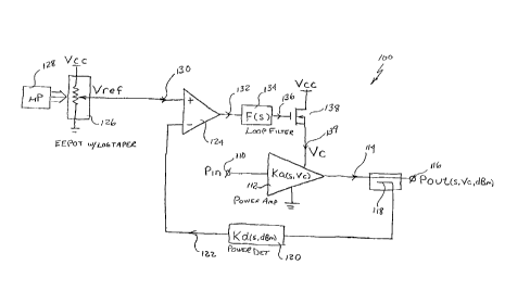
Referring now to Fig. 2, a linear power control loop 100 of the present
invention is depicted. Linear power control loop 100 eliminates the need for a
linearization circuit for the power detector and provides a wide dynamic range
of
control, e.g., a linear transfer function of dB per adjustment step, by
utilizing a non-
linear reference to control a power amplifier's output power. Further, this
wide
dynamic range of control may be provided over a wide range of temperatures,
e.g.,
over 125° C. As such, linear control loop 100 of the present invention
can be used
with substantially all power amplifiers when linear control in terms of dBm
versus
linear adjustment setting is desired.
An RF signal is introduced to the linear power control loop 100 via input
terminal 110 which is coupled to a controlled RF power amplifier 112, which
CA 02298928 2000-OS-17
9
provides an amplified RF signal, represented by arrow 114 to output terminal
116.
Coupled to the output of power amplifier 112 are a signal sampler 118 and a
power
detector 120. And, unlike the prior art, power detector 120 provides an output
signal,
represented by arrow 122, directly to a summing amplifier 124; no additional
circuitry
is used in between power detector 120 and summing amplifier 124 to linearize
output
signal 122. The other input to summing amplifier 124 also differs
significantly from
the prior art in that it is provided by an electrically erasable potentiometer
(EEPOT)
126, e.g., an E2POT manufactured by Xicor or other suitable EEPOTs, which can
be
programmed by a microprocessor 128. The EEPOT output voltage, represented by
arrow 130, is compared with signal 122 to produce an error signal 132 at the
output of
summing amplifier 124. Error signal 132 is filtered by loop filter 134 which
also sets
the closed loop bandwidth of the loop. The output signal of loop filter 134,
represented by arrow 136, is tied to the gate of a biasing n-channel MOSFET
138.
The drain of MOSFET 138 is connected to a voltage source, VCS, while the body
of
MOSFET 138 is tied to its source and provides the biasing control voltage V~,
represented by arrow 139, to power amplifier 112. As such, linear power
control loop
100 operates as a closed loop to produce a linear output by forcing a null
condition,
with exponential signals, at summing amplifier 124 such that output signal 122
of
power detector 120, i.e., the feedback voltage, equals output 130 of EEPOT,
i.e., the
loop reference voltage.
Signal sampler 118 is of a standard configuration as is known in the art.
Power detector 120, however, is preferably of the configuration as depicted in
Fig. 3.
Power detector of Fig. 3 is a temperature compensating power detector, which
additionally incorporates a current source 146 and a multiplier circuit 200.
Power
CA 02298928 2000-OS-17
detector 120 includes a coupling capacitor 140 that is connected between
sampled
power input 142 and node 144. A current source 146 is also coupled to node 144
which is connected to node 154 which is connected to anode 156 of temperature
compensation diode 158. Cathode 160 of temperature compensation diode 158 is
5 connected to ground 162. A resistor 164 is connected between node 144 and
node
166 while a capacitor 168 is connected between node 166 and ground 162. A
resistor
170 is connected between node 166 and a node 172. Node 172 is fed to the
inverting
input of amplifier 174. A feedback resistor 176 connects node 172 and voltage
output
178 of amplifier 174. A capacitor 180 is connected between node 154 and ground
10 162. And, a resistor 182 is connected between node 154 and the non-
inverting input
of amplifier 174. A capacitor Ccomp 177, connects node 172 and voltage output
178
at amplifier 174.
As shown, detector diode 150 and temperature compensation diode 158 are in
DC series with each other allowing the same current to flow through both
diodes and,
thus, developing a substantially identical voltage drop across both diodes.
Optimal
performance, i.e., closer matching of the voltage drop across the diodes, can
be
achieved if matching diodes in the same package are used. Resistors 170, 176,
and
182 are preferably selected such that R, ~o=Rl ~6=R, g2. The preferred
component
values are provided below in Table 1, of course, other component values may be
used
without departing from the spirit or scope of the invention.
Table 1.
Capacitor 140 18 picoFarads
Resistor 164 360 Ohms
CA 02298928 2000-OS-17
11
Capacitor 168 22 picoFarads
Capacitor 180 1000 picoFarads
Ccomp 177 47 picoFaxads
Resistor 170, 176, 182 100 kiloOhms
Thus, the affect on power detector output voltage 178 due to a change in
voltage drop across diodes 150 and 158 due to temperature variation may be
determined by reviewing power detector 120 in a static state, i.e., no power
input.
The detector output voltage is defined as follows:
~~ = R 176 ~ylaa ~+ vlsa 8176 + 1 Eq. 1
170 170
where, in the static state:
V 44 = 2Vo and Vlsa = Yn .
Note that V~4q 1S the voltage at node 144, V,s4 is the voltage at node 154,
and Vp is
the voltage across one diode. Knowing that R1~6=Ri7o and substituting Vlaa and
Vls4,
Equation 1 becomes:
V~, _ -2V~ + 2V" = 0 Eq. (2)
Thus, the change in diode voltage due to temperature change is canceled out,
allowing
power detector 120 to provide a true voltage output that is unaffected by
temperature.
It should be noted that, while power detector 120, as shown in Fig. 3, is the
preferred
embodiment of a power detector, other suitable power detectors 120 may be used
without departing from the spirit or scope of the invention.
CA 02298928 2000-OS-17
12
Fig. 4 provides a plot that is representative of the operation of power
detector
120. The plot depicts power detector output voltage versus power input in dBm
at the
temperatures of
-40°C, -15°C, +10°C, +35°C, +60°C, and
+85°C. As the plot indicates, the output
voltage is substantially consistent for a given power input over the range of
temperatures. The plot also indicates that as the power into power detector
120
increases, the voltage level of signal output 122 of power detector 120
increases
exponentially.
Current source 146 for power detector 120, shown in Fig. 3, may be described
as follows. First, current source 146 preferably includes an inductor 184
connected
between node 144 and the collector of a pnp transistor 186. The base of
transistor 186
is tied to node 188. A resistor 190 is tied between node 188 and ground 162.
The
collector of a second pnp transistor 192 is also tied to node 188. The base of
transistor 192 is connected to a node 194. A resistor 196 is connected between
node
1 S 194 and a positive voltage supply 197, i.e., +5 volts. A resistor 198 is
provided
between positive voltage supply 197 and the emitter of transistor 192. The
preferred
component values for current source 146 are provided below in Table 2, of
course,
other component values may be used without departing from the spirit or the
scope of
the invention.
CA 02298928 2000-OS-17
13
Table 2.
Inductor 184 18 milliHenries
Resistor 190, 198 200 kiloOhms
Resistor 196 240 kiloOhms
With the component values of Table 2, current source 146 is able to provide
power
detector 120 with a bias current of approximately 10 microAmps. It should be
noted
that other current sources may be used without departing from the spirit or
scope of
the invention.
Along with current source 146, power detector 120 preferably utilizes a
multiplier circuit 200, as shown in Fig. 3. Multiplier circuit 200 includes a
resistor
202 connected between voltage output 178 of amplifier 174 and the non-
inverting
input of an amplifier 204. A resistor 206 is connected between a node 207 and
ground 162. Node 207 is coupled to the inverting input of amplifier 204. A
feedback
resistor 208 is connected between node 207 and output signal 122. The
preferred
component values of multiplier circuit 200 may be found in Table 3, of course,
other
component values may be used without departing from the spirit or scope of the
invention.
Table 3.
Resistor 202, 206 10 KiloOhms
Resistor 208 20 KiloOhms
CA 02298928 2000-OS-17
14
With the component values of Table 3, multiplier circuit 200 operates to
multiply, by
a factor of approximately three, output signal 178 to place the voltage of
output signal
122 within the output range of EEPOT 126, e.g., approximately 0 to 4.5 volts.
The total contribution from power detector 120, with reference to Fig. 3, to
linear power control loop performance, in terms of frequency and input power,
may
be defined as follows:
Eq. (3)
K~, (s, dBm) = KD ~dBm~ * 1 * G * A« (s) * A« (s~
sz~l +l sz~z +1 1+A«(s)+ G 1+A~(s)* Rzo6
s z~z + 1 Rzo6 + Rzos
where:
K" (dBm) _ °VDET ~Pwr) , where Vo~T(Pwr) is the non-linear transfer
function of the
a(Pwr)
power detector 120 (units are in Volts/dBm),
G - 8176 _ 2~Uinde150
' zdl - I + 8164 0168 ~
170 Bias
_ GBP
~OL - ~ ~d zd 2 = CComp 8176 '
AoL
Note that GBP is the gain bandwidth product of amplifier 174 and AoL is the
open-
circuit DC voltage gain of amplifier 174.
Referring once again to Fig. 2, it can be seen that EEPOT 126 provides its
output 130 to summing amplifier 124. EEPOT 126 is preferably one with a
logarithmic taper having a dynamic range of 30 dB or more. A Xicor, Inc.,
digitally
controlled potentiometer having Model No. X9314 has been found to be a
suitable
EEPOT 126, of course, other EEPOTs may be used without departing from the
spirit
CA 02298928 2000-OS-17
of scope of the invention. An EEPOT 126 is typically implemented by a resistor
array
composed of multiple resistive elements and a wiper switching network. Between
each resistive element and at either end are tap points accessible to the
wiper terminal.
The position of the wiper is controlled by microprocessor 128. The high and
low
5 terminals of EEPOT 126 are equivalent to the fixed terminal of a mechanical
potentiometer. The maximum and minimum voltages out of EEPOT 126 are
preferably set to approximately 4.6 and 0 volts, respectively. Note that this
range
corresponds to the range of the voltage signal output 122 of power detector
120. As
such, the resistance of EEPOT 126 and its corresponding output voltage signal
130
10 are adjustable in thirty-two incremental steps (between approximately 0 and
4.6
volts), of course, other resistance ranges and the number of incremental steps
may be
used without departing from the spirit or scope of the invention.
Fig. 5 provides a plot that is representative of the voltage level of EEPOT
output signal 130 as the resistance of EEPOT 126 is adjusted. As the plot
indicates,
15 output voltage signal 130 increases exponentially as the resistance of
EEPOT 126 is
increased linearly.
Referring to Fig. 6, a circuit diagram of the preferred embodiment of summing
amplifier 124 and loop filter 134 is provided. As shown, a summing amplifier
has
been implemented within a circuit that has been configured to also act as the
loop
filter, with a single pole response, as well as a summer. As such, the
combination
summing amplifier/loop filter 137 may be described as follows. First is a node
212
which receives output voltage signal 122. Connected between node 212 and a
node
216 is a resistor 214. Node 216 is fed to the inverting input of operational
amplifier
225. A parallel combination of a resistor 218 and a capacitor 220 is provided
between
CA 02298928 2000-OS-17
16
node 216 and the output 236 of summing amplifier/loop filter 137. A node 222
receives output voltage signal 130. Connected between node 222 and a node 224
is a
resistor 226. Connected between node 224 and ground 162 is a parallel
combination
of a resistor 228 and a capacitor 230. Node 224 is fed to the non-inverting
input of
operational amplifier 225. The preferred component values of summing
amplifier/loop filter 137 are provided below in Table 4, of course other
component
values may be used without departing from the spirit or scope of the
invention.
Table 4.
Resistor 214, 226 160 Ohms
Resistor 220, 228 200 kiloOhms
Capacitor 220, 230 0.1 microFarads
Operational amplifier 124 operates to provide an error voltage output 236 that
is
representative of the difference in voltage between output voltage signal 122
and
output voltage signal 130, i.e., V 122-V 130. Loop filter operates as a low
pass filter
acting to stabilize the error voltage signal to power amplifier 112.
The total transfer function of the summing amplifier/loop filter 137, with
reference to Fig. 6, in respect to linear power control loop performance, in
terms of
frequency, may be defined as follows:
G AoLZ Cs)
q~ ~ )
F~s~= sz +1 * 1+A~,LZ~s~+ G E 4
s z, + 1
where:
~~I
CA 02298928 2000-OS-17
17
Aorz Cs) = S oLZ ~ G = Rzis ~ z~ = Rz~sCzzo ~ and
/~ + 1 Rzia
~OL 2
GBP2
~oa z =
AoLz
Note that GBP2 is the gain bandwidth product and AoL2 is the open-circuit DC
voltage gain of amplifier 174.
Referring once again to Fig. 2, output 136 of loop filter 134 is tied to the
gate
of MOSFET 138. MOSFET 138 provides the biasing control voltage 139 to power
amplifier 112.
The transfer function of the power amplifier 112 in respect to linear power
control loop performance, in terms of the control voltage, V~, may be defined
as
follows:
Ku~s~v'v=KA~V~O* 1 Eq~ (5)
s z"a~., + 1
where:
( aPo~, ~V~.oNr J ~d z 1
Ka IVC, ~ _ _
a(VcoNr) ""''' 2~(timeconst.~'
where Pot,7. (Y~.«Nr ~ is the non-linear transfer function of the power
amplifier (units are
in dBm/volts). The time constant is from the frequency response of MOSFET 138.
As such, in view of the above, the closed loop response of the linear power
control loop 100 includes the transfer function of power amplifier 112 and the
transfer
function of power detector 120, and may be defined as follows:
Ku (s~ YcoNr ) * F(s
Poor ~s~ dBm, V~.~~N~. ~ = 1 + F(s~ * Ku (s, ycoNT ~ * Ka (s~ dBm~ Eq~ (6)
CA 02298928 2000-OS-17
18
where F(s) has been defined as summing amplifier/loop filter 137.
In view of the above, it can be seen that linear power control loop 100
operates
as a closed loop to produce a linear output 116 by forcing a null condition,
with
exponential signals, at summing amplifier 124 such that the output signal of
power
detector 120, i.e., the feedback voltage, equals the output 130 of EEPOT 126,
i.e., the
reference voltage. Fig. 7 provides a plot depicting operation of linear power
control
loop 100. The plot depicts linear power control loop output 116 in dBm versus
the
wiper terminal setting, e.g., adjustment step, of EEPOT 126 at the
temperatures of -
40°C, -10°C, +25°C, +60°C, and +85°C. As
the plot indicates, linear power control
loop output 116 is substantially linear per linear adjustment of the wiper
terminal of
EEPOT 126, i.e., per stepped up increase in resistance of EEPOT.
The present invention may be embodied in other specific forms without
departing from the spirit of the essential attributes thereof; therefore, the
illustrated
embodiments should be considered in all respects as illustrative and not
restrictive,
reference being made to the appended claims rather than to the foregoing
description
to indicate the scope of the invention.