Note: Descriptions are shown in the official language in which they were submitted.
CA 02299122 2000-02-23
OXIDE PHOSPHOR ELECTROLUMINESCENT LAMINATE
FIELD OF THE INVENTION
The present invention relates to electroluminescent laminates that
include a thin film electroluminescent oxide phosphor layer.
BACKGROUND OF THE INVENTION
Thin film electroluminescent (TFEL) devices typically include a
laminate or laminar stack of thin films deposited on an insulating substrate.
The thin films include a transparent electrode layer and an electroluminescent
(EL) phosphor structure, comprising an EL phosphor material sandwiched
between a pair of insulating layers. A second electrode layer completes the
laminate structure. In matrixed addressed TFEL panels the front and rear
electrodes form orthogonal arrays of rows and columns to which voltages are
~5 applied by electronic drivers, and light is emitted by the EL phosphor in
the
overlap area between the rows and columns when sufficient voltage is applied
in excess of a voltage threshold.
In designing an EL device, a number of different requirements have to
be satisfied by the laminate layers and the interfaces between these layers.
2o To enhance electroluminescent performance, the dielectric constants of the
insulator layers should be high. To work reliably however, self-healing
operation is desired, in which electric breakdown is limited to a small
localized
area of the EL device: The electrode material covering the dielectric layer
fails
CA 02299122 2000-02-23
at the local area, preventing further breakdown. Only certain dielectric and
electrode combinations have this self-healing characteristic. At the interface
between the phosphor and insulator layers, compatibility between materials is
required to promote charge injection and charge trapping, and to prevent the
interdiffusion of atomic species under the influence of the high electric
fields
during operation.
Standard EL thin film insulators, such as Si02, Si3N4, AI203, SiOxNy,
SiAIOXNy and Ta205 typically have relative dielectric constants (K) in the
range
of 3 to 60 which we shall refer to as low K dielectrics. These dielectrics do
o not exhibit the properties required to work well in layers adjacent to oxide
phosphors, which have high threshold electric fields. A second class of
dielectrics, called high K dielectrics, hold more potential. This class
includes
materials such as SrTi03, BaTi03, PbTi03 which have relative dielectric
constants in the range of 100 to 10,000, and are crystalline with the
~5 perovskite structure. While all of these dielectrics exhibit a sufficiently
high
figure of merit (defined as the product of the breakdown electric field and
the
relative dielectric constant) to function in the presence of high electric
fields,
not all of these materials offer sufficient chemical stability and
compatibility in
the presence of high processing temperatures and/or high electric fields.
2o SrTiOa, BaTi03, exhibit the required properties to provide good performance
in an EL device, when positioned adjacent to oxide phosphors.
In view of the multiple and often conflicting requirements placed on the
insulating layers and their interfaces, multicomponent insulator structures
2
CA 02299122 2000-02-23
have been proposed. Also, it is known in the art that SrTi03, BaTi03 can be
used in EL devices. For example, United States Patent No. 4,857,802 to
Fuyama discusses the use of SrTi03 and BaTi03 insulating layers. However,
this teaches how to grow the pervoskite structure dielectrics in a [111]
orientation to improve its breakdown strength, and only discusses application
with sulfide phosphors. The compatibility issues with oxide phosphors, and
the incorporation of self-healing breakdown functionality is not addressed.
United States Patent No. 4,547,703 to Fujita teaches the use of a
multi-layer insulator comprised of non-self healing dielectric layers combined
with self healing dielectric layers. In this case, a self-healing, low K
dielectric
is adjacent to the sulfide phosphor, and the primary rationale for including
the
non-self healing dielectric in the EL device was to increase the capacitance
of
the insulating layer, thereby increasing the electric field in the phosphor
and
increasing the charge transfer into the phosphor during emission. The
~5 rationale did not include providing electrical and chemical compatibility
with
the phosphor.
United States Patent No. 4,897,319 to Sun teaches the use of a multi-
layered insulator in an EL device. However, in Sun's devices, no high K
dielectrics are employed, and he teaches that it is essential to have a SiON
20 layer (a low K dielectric) adjacent to the sulfide phosphor.
Thus, two component insulators have been proposed in which a low
dielectric constant material maintains the charge trapping and injection at
the
interface with the phosphor, and a high dielectric constant material layer
3
CA 02299122 2000-02-23
increases the electric field in the phosphor. A high dielectric constant layer
increases the field in the phosphor, and a low dielectric constant layer
interfaces with an electrode to promote self healing electrical breakdown.
The teachings of the prior art on TFEL structures are based on the use
of doped zinc sulfide as the EL phosphor layer. It would be very
advantageous to provide a TFEL device that uses electroluminescent oxides
instead of sulphides since the former are less sensitive to atmospheric water
vapor and oxygen and so minimal sealing is required in manufacturing the
display. Since the interface characteristics between the insulator layer and
the
phosphor are important in designing a successful EL structure, prior art is
not
particularly helpful in developing a TFEL stack which uses unrelated material
formulations as the EL phosphor layer. While SrTi03 and BaTi03 exhibit
desirable interface and charge injection properties with oxide phosphors, they
also exhibit propagating breakdown mode in thin films.
~5 Therefore, it would be very advantageous to provide thin film
electroluminescent structures which use oxide based electroluminescent
phosphors and which provide a self-healing breakdown mode of operation. A
more electrically robust dielectric layer with a high figure of merit is
required
adjacent to the phosphor to provide proper electron trapping and charge
2o injection in the presence of high electric fields. At the same time, the
material
must not react with the phosphor during high temperature processes in
manufacture, nor allow chemical reaction or inter-diffusion of chemical
species between the phosphor or the adjacent layer in the presence of these
4
CA 02299122 2000-02-23
high electric fields. Because both bulk and surface properties are important,
this is known as the dielectric interface layer.
SUMMARY OF THE INVENTION
It is an object of the present invention to develop thin film EL device
structures that include the oxide phosphors.
To achieve this objective, thin film SrTi03 and BaTi03 have been
employed next to the oxide phosphor layer (on one or both sides of the oxide
layer), primarily as stable charge injection, and trapping interface layers,
and
to increase the electric field in the phosphor. Electric breakdown protection
through self-healing has been provided by traditional low K dielectrics in
combination with an appropriate choice of adjacent electrode. The high
dielectric constant materials employed also provide for a high capacitance
layer, thereby increasing the electric field in the phosphor and increasing
the
~5 charge transfer into the phosphor during emission.
In one aspect of the invention there is provided an electroluminescent
laminate, comprising;
an electrically insulating substrate;
a conducting metal oxide layer on a surface of the substrate;
2o an electroluminescent oxide phosphor layer on the conducting layer;
a first dielectric interface layer on the oxide phosphor layer;
a first dielectric layer on the first dielectric interface layer, the first
dielectric interface layer having a dielectric constant higher than a
dielectric
5
CA 02299122 2000-02-23
constant of the first dielectric layer; and
a second conducting layer on the first dielectric layer, and wherein at least
one of the conducting layer and the conducting metal oxide layer is
substantially
transparent, and wherein when only the conducting metal oxide layer is
substantially transparent the substrate is also transparent. In this aspect of
the
invention the first dielectric layer and the second conducting layer are
characterized by self healing properties.
In another aspect of the invention there is provided an electroluminescent
laminate, comprising;
o an electrically insulating substrate;
a first conducting layer on a surface of the substrate;
a first dielectric interface layer on the first conducting layer;
an oxide phosphor layer on the first dielectric interface layer;
a second dielectric interface layer on the oxide phosphor layer;
~5 a first dielectric layer on the second dielectric interface layer;
the first and second dielectric interface layers each having a dielectric
constant greater than a dielectric constant of the first dielectric layer; and
a second conducting layer on the first dielectric layer, and wherein at least
one of the two conducting layers is substantially transparent, and wherein
when
20 only said first conducting layer is substantially transparent said
substrate is also
transparent.
In this aspect of the invention the first dielectric layer and the second
conducting layer are characterized by self-healing properties.
6
CA 02299122 2000-02-23
BRIEF DESCRIPTION OF THE DRAWINGS
The invention will now be described, by way of example only, reference
being had to the accompanying drawings, in which:
Figure 1 a is a cross sectional view of a first embodiment of a structure of
a thin film electroluminescent (TFEL) device constructed in accordance with
the
present invention;
Figure 1 b is a cross sectional view of an alternative embodiment of a
structure of a TFEL device;
Figure 1 c is a cross sectional view of another alternative embodiment of
o a structure of a TFEL device;
Figure 2 is a cross sectional view of a TFEL device based on the structure
of Figure 1 a ;
Figure 3 is a graph showing both brightness and efficiency versus voltage
of electroluminescence obtained from the device of Figure 2;
~5 Figure 4 is a cross sectional view of a TFEL device based on the structure
of Figure 1 b; and
Figure 5 is a graph showing both brightness and efficiency versus voltage
of electroluminescence obtained from the device of Figure 4.
2o DETAILED DESCRIPTION OF THE INVENTION
The inventors have shown for the first time that thin film dielectrics may
be used to form bright EL laminate devices using oxide phosphors. These oxide
phosphors require different properties from the layers adjacent to the
phosphor
7
CA 02299122 2000-02-23
than do the traditional EL sulfide-based phosphors. Oxide phosphors require
higher electric fields than do traditional EL phosphors based on sulfides.
These
high operating fields, combined with the higher processing temperatures of
oxide
phosphors (600°-800°C) and the fact that these oxide phosphors
have a
different fundamental chemical composition compared to sulfides create some
challenges to overcome when making an oxide-phosphor based EL device.
Being all thin-film in nature, the devices produced according to the
present invention demonstrate steep brightness-voltage behavior and have been
prepared on glass, and fused silica substrates. A variety of common substrates
can be used including glass, fused silica, ceramic glass and glazed or
polished
ceramic.
Corning 1737 substrates, coated by a commercial supplier Applied Films
Inc. with a conducting bottom electrode layer comprising indium tin oxide
(ITO)
to a thickness of ~1500A by RF sputtering are coated with a series of
dielectric,
~5 EL and top electrode layers. Non-limiting examples will be given
hereinafter of
devices formed on glass and their behavior to illustrate the structure and
resulting performance available. All layers are grown by RF sputter deposition
except for the aluminum rear electrode which is thermally evaporated.
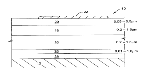
Referring first to Figure 1 a, a structure of a TFEL device shown generally
2o at 10 includes a substrate 12 onto which a conducting electrode 14 is
deposited.
A high dielectric constant interface layer 26 is deposited on the electrode
14. An
oxide phosphor layer 16 is sandwiched between the dielectric interface layer
26
and another dielectric interface layer 18. Another dielectric layer 20 is
located
8
CA 02299122 2000-02-23
on top of dielectric interface layer 18. Dielectric interface layers 18 and 26
are
high K materials. An electronically conducting electrode 22 is located on top
of
dielectric layer 20 to form a self-healing structure. The preferred thickness
ranges for each of the layers comprising the TFEL structure 10 is shown to the
right of the corresponding layer in Figure 1a. One or both of the electrodes
is
transparent. If only the lower electrode is transparent, the substrate is also
transparent.
Preferred low dielectric materials for use in the present invention include
thin film dielectrics, such as Si02, Si3N4, AI203, SiOXNY, SiAIOXNy and Ta205
that
have relative dielectric constants K in the range of 3 to 60. These
dielectrics do
not exhibit the properties required to work well in layers adjacent to oxide
phosphors. A second class of dielectrics having higher dielectric constants
and
functioning as both a dielectric and a charge injection layer is located
directly on
the oxide phosphor layer. These dielectrics include materials such as SrTi03
and
~5 BaTi03 which have relative dielectric constants in the range of 100 to
5,000, and
are crystalline with the perovskite structure.
An alternative embodiment of a structure of a TFEL device is shown at 30
in Figure 1 b. TFEL structure 30 is similar to structure 10 in Figure 1 a but
the
dielectric interface layer 26 is removed. While this embodiment does not have
2o a dielectric interface layer between the phosphor and an electrode, certain
electrode materials (such as ITO and Zn0) do provide the characteristics
necessary for a functioning TFEL device. The preferred thickness ranges for
each of the layers comprising the TFEL 30 structure is shown to the right of
the
9
CA 02299122 2000-02-23
corresponding layer in Figure 1 b.
Another alternative embodiment of a structure of a TFEL device is shown
at 40 in Figure 1 c. TFEL structure 40 is similar to structure 10 in Figure 1
a but
additionally includes a low dielectric constant layer 28 interposed between
lower
electrode 14 and the dielectric interface layer 26. The preferred thickness
ranges
for each of the layers comprising the TFEL structure 40 is shown to the right
of
the corresponding layer in Figure 1 c.
A TFEL device based on the laminate structure of Figure 1 a is shown at
50 in Figure 2. Corning type 1737 glass was used as a substrate 12. The glass
1o substrate 12 was 1.1 mm thick and was coated with an electronically
conducting
bottom electrode 14 comprising indium tin oxide (ITO) deposited by RF
magnetron sputtering to a thickness of approximately 1500 A by Applied Films
Inc. Next, a SrTi03 layer was sputtered by RF sputtering from a SrTi03 target
to
form a 500A thick dielectric interface layer 26 on top of the electrode layer
14.
The substrate temperature was held at 550°C. An oxide thin film EL
phosphor
layer 16 was then sputter deposited from an oxide target comprising
Zn2Sio.5Geo.504:Mn by RF magnetron sputtering. The substrate temperature was
held at 250°C and the EL film thickness was about 8000A. The laminate
was
baked at 700°C for 1 hour in vacuum to activate and crystallize the
phosphor
layer 16. Next, SrTi03 was sputtered by RF sputtering from a SrTi03 target to
form a 9000A thick dielectric interface layer 18 on top of the EL oxide
phosphor.
The substrate temperature was held at 550°C. The dielectric SiAION
layer 20
was then sputter deposited to a thickness of 1000A with the substrate held at
CA 02299122 2000-02-23
100°C. Finally, an aluminum electrode 22 was thermally evaporated to a
thickness of 700A on top of the SiAION.
The performance of the TFEL device of Figure 2 is illustrated in Figure 3.
AC pulses were applied to the device at a frequency of 225 Hz. The threshold
voltage is 210 volts and the brightness reaches 185 fL at a voltage of 250
volts.
The maximum efficiency is above 0.5 I/V1/.
Another type of layer that exhibits the required properties for good EL
performance when positioned adjacent to the oxide phosphors is a conducting
oxide such as indium tin oxide or zinc oxide, which are both transparent.
These
layers provide charge injection and are chemically stable, but may result in
EL
performance that is somewhat lower than the use of SrTi03 or BaTi03. An
advantage to the use of the conducting, transparent oxide layer is the
elimination
of one layer in the EL laminate. The dielectric layer 20 and the conducting
electrode 22 are chosen to form a self-healing structure. Figure 4 shows a
modified laminate structure at 60 which is similar to the TFEL structure in
Figure
1 b in which the oxide phosphor is located on an indium tin oxide (ITO) layer.
The
performance of the TFEL device of Figure 4 is illustrated in Figure 5. AC
pulses
were applied to the device at a frequency of 60 Hz. The threshold voltage is
200
volts, and a brightness of 50fL is achieved at 240 volts. The maximum
efficiency
is 0.4 L/V1/.
The non-limiting exemplary results shown in Figures 2 to 4 were obtained
using the electroluminescent green phosphor Zn2SiXGe~-X04:Mn, wherein 0 <_ x
< 1 with a preferred value of x being about 0.5. Mn is preferably present in
the
11
CA 02299122 2000-02-23
range from about 1 % to 4% mole. The presence of germanium in the zinc
germanates produces a very efi'ICient green electroluminescent phosphor and
has the effect of lowering the processing temperatures to well below a
thousand
degrees as disclosed in United States Patent Nos. 5,725,801, 5,788,882 and
5,897,812 which are each incorporated herein by reference in their entirety.
These patents also disclose highly efficient oxide based red emitting
phosphors, discussed hereinafter, which may also be incorporated into the TFEL
devices disclosed herein (data not shown). The red phosphors that may be used
in the present TFEL laminates may include Ga203:Eu with Eu spanning the range
1o in which said rare earth is soluble in Ga203 and is preferably in a range
from
about 0.1 % to about 12%. Another EL oxide that may be used is Ca,_XEuXGayOz,
where x is in the range from about 0.001 to about 0.1, y is in a range from
about
0.5 to about 4, and z is approximately equal to 1+(3/2)y.
Another electroluminescent red emitting phosphor that may be used has
a formulation given by Sr,-XEuXGayOZ, where x is in the range 0.001 to 0.1, y
is
from about 0.5 to about 12, and z is approximately 1+(3/2)y.
Another electroluminescent red emitting phosphor film that may be used
has a formulation given by Ba,_XEuXGayOZ, where x is in the range from about
0.001 to about 0.1, y is from about 0.5 to about 4, and z is approximately
1 +(3/2)y.
A red emitting phosphor oxide compound having a formula
Sr3Ga206:n%Eu, wherein n% is the mole percent of Eu present in Sr3Ga206 and
spans the range in which Eu is soluble in Sr3Ga206 may be used. Another red
12
CA 02299122 2000-02-23
emitting phosphor that may be used includes the compound having a formula
Sr4Ga20,:n%Eu, wherein n% is the mole percent of Eu present in Sr4Ga20, and
spans the range in which Eu is soluble in Sr4Ga20,. Another red emitting
phosphor compound that may be used has a formula Sr,Ga40,3:n%Eu, wherein
n% is the mole percent of Eu present in Sr,Ga40~3 and spans the range in which
Eu is soluble in Sr,Ga40~3.
Another electroluminescent red phosphor that may be used is
SrGa204:n%RE wherein RE is a rare earth dopant selected from the group
consisting of Eu, Tb and combinations thereof, n% is the mole percent of RE
1o present in SrGa204 and spans the range in which the rare earths are soluble
in
SrGa204,
Other red emitting compounds that may be used include a compound
having a formula SrGa40,:n%Eu, wherein n% is the mole percent of Eu present
in Sr4Ga20, and spans the range in which Eu is soluble in Sr4Ga20,; a
compound having a formula SrGa,20,9:n%Eu, wherein n% is the mole percent
of Eu present in SrGa,20,9 and spans the range in which Eu is soluble in
SrGa,20,9; a compound having a formula Sr3Ga409:n%Eu, wherein n% is the
mole percent of Eu present in Sr3Ga409 and spans the range in which Eu is
soluble in Sr3Ga409; a compound having a formula Ba3Ga206:n%Eu, wherein n%
2o is the mole percent of Eu present in Ba3Ga206, and spans the range in which
Eu
is soluble in Ba3Ga206; a compound having a formula Ba4GaZO,:n%Eu, wherein
n% is the mole percent of Eu present in Ba4Ga20,, and spans the range in which
Eu is soluble in Ba4Ga20,.
13
CA 02299122 2000-02-23
Another red emitting electroluminescent oxide phosphorthat may be used
in the present laminate includes the electroluminescent phosphor having a
formula BaGa204:n%RE, wherein RE is a rare earth dopant selected from the
group consisting of Eu, Tb, and combinations thereof, n% is the mole percent
of
RE present in BaGa204 and spans the range in which said rare earths are
soluble in BaGa204.
These oxide phosphors are highly advantageous because, as disclosed
in these patents, they have demonstrated high luminance output and extended
life. Further, being oxides, they do not react with atmospheric water vapor
and
oxygen and so minimal sealing is required in manufacturing the display.
Other oxide phosphors may also be employed, such as those containing
other rare earth dopants which emit light of other colours such as Tb, Dy, Tm
or
transition metal dopants such as Ti and Cr. Since the achievement of a full
range
of colours is important for EL devices, the range of EL oxide phosphors that
may
be employed in the current laminate is not to be restricted.
It will be understood that the thickness in the Figures are not meant to be
limiting but serve to exemplify how the present EL devices may be made using
all thin ~Ims which is a major advantage of the present invention.
The inventors have shown for the first time that bright red and green oxide
2o phosphors may be incorporated in TFEL device structures using much thinner
dielectric layers in the thickness range from submicrons to several microns.
Those skilled in the art will appreciate that the TFEL structures comprising
the
conducting electrode layers, phosphors and dielectrics may be deposited in a
14
CA 02299122 2000-02-23
variety of methods that are well known in the TFEL literature as applied to
sulfide
phosphors, see for example Y. Ono, "Electroluminescent Displays", World
Scientific, 1995, Singapore. A range of substrates may also be used including
glass, fused silica, ceramic glass and glazed or polished ceramic. In
addition,
those skilled in the art will understand that there are many alternative
dielectric
materials that may be used, for example, high K dielectrics such as BaTi03, or
low K dielectrics such as Ta205, Y203, aluminum titanate, silicon oxy-nitride
and
silicon aluminum oxy-nitride. A partial list of dielectrics which may be used
in the
devices disclosed herein is found in Ono.
1o The foregoing description of the preferred embodiments of the invention
has been presented to illustrate the principles of the invention and not to
limit the
invention to the particular embodiment illustrated. It is intended that the
scope
of the invention be defined by all of the embodiments encompassed within the
following claims and their equivalents.
15