Note: Descriptions are shown in the official language in which they were submitted.
CA 02299345 2000-02-07
WO 99/09455 1 PCT/US98/16680
MULTI PARAMETER SCANNER
S
CROSS REFERENCE TO RELATED APPLICATIONS
This application is a Continuation-In-Part of U.S. Provisional
Application Serial No. 60/055,567, the complete disclosure of which is
incorporated
herein by reference for all purposes. This application is related to commonly
assigned
to U.S Patent Nos. 5,591,981, issued January 7, 1997 and 5,266,803, issued
November 30,
1993 and to commonly assigned, co-pending U.S. Patent Application Nos.
08/585,303,
filed January 11, 1996, 08/729,111, filed October 1 l, 1996, and to
08/927,556, filed
September 9, 1997, the complete disclosures of which are incorporated herein
by
reference for all purposes.
FIELD OF THE INVENTION
The present invention relates generally to optical scanners and, more
particularly, to a method and apparatus for measuring and/or imaging
biological or
other types of samples that have been labeled using a variety of techniques.
BACKGROUND OF THE INVENTION
Imaging is an important tool used in the detection of a variety of
biological molecules. For example, imaging devices may be used to detect and
determine concentrations of molecules of a specific molecular weight, DNA, a
specific
DNA sequence, proteins, and carbohydrates. Typically the samples of interest
are
labeled using fluorescent dyes, radioisotopes, or enzyme activated light
emitting (i.e.,
chemiluminescent) or fluorescent (i.e., chemifluorescent) chemicals.
UV, visible or IR light excites fluorescent dyes and markers. Once
excited the dyes fluoresce, preferably emitting light at a wavelength
distinguishable
3o from the excitation wavelength. Radioactive and chemiluminescent signals
are
typically captured using either x-ray film or storage phosphor screens. The x-
ray film
is developed and read using a densitometer. The storage phosphor screen does
not
require development and is read out by scanning the screen with a beam of
light. The
readout beam produces an emission from the storage phosphor, the intensity of
the
CA 02299345 2000-02-07
WO 99/09455 2 PCT/US98/16680
emission being proportional to the original quantity of radiation retained by
the storage
phosphors.
A variety of devices have been described for use in detecting labeled
biological samples. U.S. Patent No. 3,746,840 discloses a device for high-
resolution
readout of information stored on a film. The device comprises a slit equal in
width to
the desired resolution with optical fibers behind the slit of a diameter equal
to the slit
width. The optical fibers collect the light as it crosses the slit and
transmits it to the
detectors.
U.S. Patent No. 3,836,225 discloses a fiber optic laser scanner. The
disclosed scanner uses two optical fiber sets attached to electromagnetic
coils. The
magnetic coils deflect the beam as required.
U.S. Patent No. 3,892,468 discloses a passive array of variable length
optical fibers that function as a dynamic scanner. Each consecutive fiber in
the fiber
array is incrementally longer than the preceding fiber. Thus light entering
the fibers at
the same time will exit the fibers at different times, the variations in exit
times thus
being correlated with different locations.
U.S. Pat. No. 4,877,966, discloses a device for measurement of
low-level laser induced phosphorescence. The laser is directed through a beam
expander and then aimed by mirrors. The induced phosphorescence is collected
by a
2o fiber optic face plate and passed to a photomultiplier tube.
U.S. Patent No. 5,062,942 discloses a fluorescence detection system for
use with electrophoresis gel plates. In the disclosed system the gel plate is
illuminated
with a laser excitation source and the emitted fluorescent light is separated
into a
plurality of virtual images that are subsequently passed through individual
bandpass
filters thereby providing multicolor fluorescence detection.
U.S. Patent No. 5,290,419 discloses a multicolor fluorescence detection
system utilizing multiple laser sources and means for detecting fluorescence
as a
function of wavelength. The individual laser sources are combined with a light
chopper
(e.g., rotary shutter) in order to irradiate the sample on a time-sharing
basis.
3o U.S. Patent No. 5,436,718 discloses a multi-function photometer for
measuring the absorbance, fluorescence, and luminescence associated with a
sample.
The disclosed system uses optical fibers to transmit light to and from the
sample using
a scanning head. A computer controlled positioning table is used to position
the
scanning head with respect to the samples contained in a microplate.
*rB
CA 02299345 2000-02-07
WO 99/09455 3 PCT/US98/16680
U.S. Patent No. 5,459,325 discloses a high-speed fluorescence scanner.
The system utilizes a lightweight scan head to scan a collimated excitation
beam across
the sample. The emitted fluorescence is gathered by the scan head lens and
directed
back along the optical path of the excitation beam to a detector. In order to
obtain a
two-dimensional image of the sample, the sample is translated in an axis
orthogonal to
the scan line.
In a publication entitled Imaging as a Tool for Improving Length and
Accuracy of Sequence Analysis in Automated Fluorescence-Based DNA Sequencing
by
Sanders et al., a method of signal analysis is disclosed. (Electrophoresis
1991, 12, 3-
11 ). In the disclosed method, a computer program was used to remove
distortions in
the DNA bands in sequencing gels, thus improving the accuracy of DNA sequence
analysis. The authors noted that the disclosed techniques should be applicable
to other
systems such as gel electrophoresis of proteins and DNA restriction fragments.
The scanners described above do not take full advantage of the wide
~5 range of different sample types available. Rather, a typical scanning
device is designed
for a specific type of sample, e.g., fluorescent samples, and as a result is
incapable of
use with another type of sample. In addition, many biological sample scanners
offer a
very limited set of irradiation/excitation wavelengths andlor emission
wavelengths, thus
further limiting the functionality of the device. Lastly, the resolution
offered by many,
2o if not all, of the fore-mentioned markers is not fully utilized by most
biological sample
scanning systems.
Therefore a compact optical scanner capable of use with a variety of
sample types and configurations that offers multiple excitation/irradiation
wavelengths
and that may be used to detect emissions at a variety of wavelengths is
desirable.
SLmdMARY OF THE INVENTION
The present invention provides an apparatus capable of measuring
quantities of biological or other types of samples that have been labeled
using any of a
variety of techniques including fluorescence, radioisotopes, enzyme activated
light
3o emitting chemicals, and enzyme activated fluorescent materials. The
apparatus allows
for either simultaneous or sequential acquisition of signals from multiple
sample types.
The apparatus is not restricted to a particular source or wavelength of
excitation or
readout light, nor is the apparatus restricted to a particular emission
wavelength. Thus
CA 02299345 2000-02-07
WO 99/09455 4 PCT/US98/16680
the present invention is capable of measuring every type of fluorescent dye,
storage
phosphor screen, and chemiluminscent probe.
In one aspect of the invention, the scanner includes a source module.
The source module has an internal laser that emits two wavelengths, 532
nanorneters
and 1064 nanometers, of approximately the same intensity. These two
wavelengths
allow the scanner to function with storage phosphor screens based on BaFBr:Eu,
SrS:Ce, and SrS:Sm as well as a variety of fluorescent dyes and other stains.
An
optional external light source may be easily coupled to the source module,
thus adding
further flexibility to the scanner's potential applications through the
addition of other
1o wavelengths in the I1V, visible, mid-IR, and IR spectral ranges. The
external light
source passes through a beam splitter that combines the emissions from the
internal
laser with those of the external source(s). The light emitted by the external
source
undergoes an auto-alignment procedure to insure optimal coupling between the
source
and the optical system of the scanner.
In another aspect of the invention, the scanner includes a detection
module. Within the detection module are two detectors, thus allowing the
simultaneous
detection of multiple wavelengths. A variety of bandpass filters and beam
splitters
contained in at least two filter wheels provide the means of removing
undesired
radiation from the light beam prior to detection. Preferably the two detectors
are photo-
2o multiplier tubes, thus providing high sensitivity over a relatively wide
wavelength
range.
A bifurcated optical cable is preferably used to transfer the excitation
and/or readout light from the source module to the sample and subsequently
transfer the
emitted and/or scattered light from the sample to the detection module.
Although
neither the number nor the physical arrangement of the fibers is critical,
typically
between I and 10 excitation fibers are surrounded by between 100 and 300
collection
fibers in order to form the scanning head probe. Coupled to the end of the
fiber
scanning probe are focussing optics and condensing optics. In order to
accommodate a
range of sample sizes without adjusting the separation distance between the
probe and
3o the sample, preferably the probe optics provide a focal spot size of less
than 150
micrometers over a 5 millimeter range. Alternatively, either the scanning head
probe or
the optics within the probe may be coupled to a translation stage, thus
allowing the
scanning probe to be optimized for different sample sizes.
CA 02299345 2000-02-07
WO 99/09455 5 PCT/US98/16680
In another aspect of the invention, the system includes a scanning stage
for scanning the probe across the sample. The system is designed to
accommodate a
variety of samples and sample types, ranging from phosphor screens, gels, and
fluorescent samples to microtiter plates. The scan head is mounted to a pair
of
s translation stages, thus allowing the probe to scan the entire available
sampling area or
some subset thereof. In one embodiment of the invention, the scanning system
operates
in a closed loop fashion, thereby providing direct position feedback.
Positional
information may be obtained using optical encoders, either mounted within the
motors
operating the translation stages or mounted in such a way as to monitor stage
travel of
1o the individual translation stages.
In another aspect of the invention, a microprocessor controls the
scanning system. In one embodiment the microprocessor controls motors coupled
to
the scanner's translation stages, thus allowing the microprocessor to control
the scan
speed as well as the sampling area of the scanner. In another embodiment the
15 microprocessor also controls the filter wheels in the source module and the
filter wheels
in the detector module. In yet another embodiment the microprocessor controls
the
high voltage supplies for photomultiplier tube detectors in the detection
module, thus
allowing the gain of the detectors to be varied depending upon the
requirements
imposed by the sample.
2o The microprocessor of the present invention may be coupled to an
external computer. The external computer may be used to change the programming
of
the microprocessor, thus allowing the system to be altered as different
detector
modules, source modules, and external sources are added to the system. The
external
computer may also be used to provide the user with a means of programming the
25 microprocessor for a specific test run, for example, for a specific sample
type and size.
In order to simplify programming, either the microprocessor or the external
computer
may include a look-up table containing a variety of operating parameters
and/or
programming instructions based on the intended conditions of operation (e.g.,
sample
type, irradiation wavelengths, detection wavelengths, etc.). The external
computer may
3o also be used for test result storage as well as providing a means of
processing and
displaying the test results. The results may be displayed in a variety of
formats,
including tabular and sample image displays. The external computer may also be
used
to present the data in a manner that is more understandable by the user, for
example,
representing different emittance intensities or wavelengths by different
colors.
CA 02299345 2000-02-07
WO 99/09455 6 PCT/US98/16680
A further understanding of the nature and advantages of the present
invention may be realized by reference to the remaining portions of the
specification
and the drawings.
BRIEF DESCRIPTION OF THE DRAWINGS
Fig. 1 schematically illustrates an overview of a scanner according to the
present invention;
Fig. 2 is an illustration of the preferred embodiment of the source;
Fig. 3 is an illustration of the preferred embodiment of the detection
l0 system;
Fig. 4 is an illustration of the scanning mechanism of the preferred
embodiment;
Fig. 5 is an expanded view of the preferred embodiment of the scan
head;
Fig. 6 illustrates the cross-section of the preferred embodiment of the
optical fiber bundle;
Fig. 7 illustrates the upper and lower enclosures for the preferred
embodiment of the invention;
Fig. 8 illustrates an end view of the lower housing enclosure shown in
2o Fig.7;
Fig. 9 illustrates one embodiment of a sample holding tray;
Fig. 10 illustrates an embodiment of a sample holding tray that includes
a light cover;
Fig. 11 illustrates a cross-section of a portion of a storage phosphor
exposure platform;
Fig. 12 illustrates an outer view of the storage phosphor exposure system
shown in Fig. 11; and
Fig. 13 illustrates an upper cross-sectional view of the storage phosphor
exposure system shown in Fig. 11.
DETAILED DESCRIPTION OF THE INVENTION
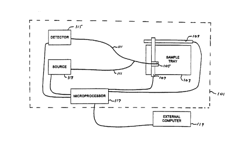
Fig. 1 schematically illustrates an overview of a scanner according to the
present invention. Although a variety of external components may be attached
to the
system for added versatility, the principal system components are designed to
fit within
CA 02299345 2000-02-07
WO 99/09455 7 PCT/US98116680
a compact; lightweight assembly 101. The sample of interest is placed on a
sample tray
103 within assembly 101. Sample tray 103 is configured to hold a variety of
sample
types, thus adding to the versatility of the device. A scanner head 105 is
movably
coupled to a pair of translation members 107 and 109. Translation members 107
and
s 109 allow scanner head 105 to be scanned over the entire sample or any
portion thereof.
An optical means 111 is coupled to scanner head 105, thereby allowing
radiation from a source 113 to pass through scanner head 105 and impinge on a
small,
selected area of the sample held in sample holder 103. Preferably optical
means 111 is
comprised of a fiber optic, thus providing a simple means of coupling energy
from
i o source 113 to scanning head 105. Light emitted and/or scattered by the
sample is
collected at head 105, passed through optical means 111, and detected by a
detection
system 115. Alternatively, light passing through the sample and reflected from
a
reflective surface placed below the sample may be collected at head 105,
passed
through optical means 111, and detected by detection system 115, thus yielding
a
15 quantity that may be correlated to the absorption of the sample.
Alternatively, the light
reflected by the sample may be collected at head 105, passed through optical
means
111, and detected by detection system 115. The means for coupling head 105 to
source
113 may be different from the means for coupling head 105 to detection system
115,
however preferably a bifurcated fiber optic is used such as that disclosed in
U.S. Patent
2o No. 5,266,803, the disclosure of which is incorporated herein in its
entirety.
A microprocessor 117, coupled to translation stages 107 and 109, is used
to control the scanning operation, for example the scan speed. Microprocessor
117 is
also coupled to source 113 and detection system i 15. Although microprocessor
117
may be configured to independently operate the scanning system, it may also be
25 coupled to an external computer system 119. External computer 119 may be
used to
program processor 117, monitor experimental progress, store test results, and
construct
and display sample images from the signals detected by system 11 S. External
computer
119 may also be used in conjunction with processor 117 to control and
manipulate the
scanning process and the resultant data (e.g., automatic lane finding,
automatic band
3o finding, automatic quantitation of results, user-defined templates for
automatic
quantitation parameters, color correction, tiling memory management, etc.).
Although source 113 may be any of a variety of source types (e.g., laser,
continuously tunable broadband source, etc.), the preferred embodiment of
source 113
is illustrated in Fig. 2. Within source 113 is a dedicated laser 201 producing
multiple
CA 02299345 2000-02-07
WO 99/09455 8 PCT/US98/16680
wavelengths. The output intensity of laser 201 may be controlled by neutral
density
filters or by digitally controlling the power supply for the laser. Preferably
laser 201 is
a diode pumped solid state laser emitting light at 532 nanometers and at 1064
nanometers. The dual wavelength capabilities of laser 201 allow a wide range
of
samples to be excited without requiring any changes to the system. In the
preferred
embodiment, either the cavity minors of laser 201 or the coatings of the laser
optics are
designed such that the laser emits approximately the same energy intensity
within the
two selected wavelengths. By providing approximately the same output power,
multiple types of phosphor screens can be efficiently scanned without
requiring
1o adjustments to the system. For example, storage phosphor screens based on
BaFBr:Eu,
SrS:Ce, and SrS:Sm may all be used with this source.
The light emitted by laser 201 is reflected by a beam combining mirror
203 into focussing assembly 205. Minor 203 is designed to efficiently reflect
both of
the wavelengths emitted by laser 201. Assembly 205 focuses the reflected beam
onto
~5 the end of fiber 207. Micro-positioners 209 and 211, coupled to laser 201
and mirror
203 respectively, are used to accurately locate the laser beam onto fiber 207,
thus
achieving the optimal transfer of energy from laser 201 through fiber 207 to
the sample.
Once laser 201 and mirror 203 have been properly located and locked into
position,
repositioning of these components is only required if one of them is
inadvertently
20 moved or if the laser beam exiting laser 201 exhibits movement as the laser
ages.
However the preferred embodiment of the system is designed to minimize if not
altogether eliminate the need for positional adjustment by the user.
In order to provide additional flexibility as well as the potential for use
with as-yet undiscovered samples and targets, the preferred embodiment of
source 113
25 provides for an external source 212. External source 212 is coupled to the
scanning
system through an external port 213. The light from the external source passes
through
port 213 to a collimating assembly 215. Collimating assembly 215 collimates
the light
from external source 212 and passes the collimated light through beam
combining
mirror 203 and focussing assembly 205 into fiber 207. The optical coatings on
mirror
3o 203 are designed to maximize reflection at the desired wavelengths emitted
by laser
201 while simultaneously maximizing transmittance of all other wavelengths,
particularly the wavelengths of potential interest for an external source.
Thus multiple
excitation wavelengths may be simultaneously transmitted through fiber 207 to
the
*rB
CA 02299345 2000-02-07
WO 99/09455 9 PCT/US98116680
sample, i.e., dual wavelengths from laser source 201 and one or more
wavelengths from
one or more external sources) 212.
A variety of external sources 212 may be coupled to external port 213.
Both lasers and broadband sources may be coupled into the scanning system,
depending upon the desired wavelength(s). Generally, the external source may
be any
source of ultraviolet (i.e., t1V), visible, near infrared (i.e., NIR), or
infrared (i.e., IR)
radiation. Thus the external source may be continuously tunable or not, pulsed
or
continuous, coherent or incoherent, and be in the form of a Laser or an arc
lamp or some
other source emitting the desired radiation.
As discussed above, dual wavelength internal laser source 201 may be
used with storage phosphor screens based on BaFBr:Eu, SrS:Ce, and SrS:Sm. In
addition, internal source 201 may be used with a variety of dyes, stains,
fluorescent,
and chemiluminescent markers, depending upon the required excitation
wavelength.
Potential dyes for use with the 532 nanometer line, and therefore not
requiring an
external source, include the following fluorescent dyes; JOE, TAMRA, ROX, HEX,
Bodipy, TRITC, CY3, Rhodamine B, and Lissamine Rhodamine. In addition, this
wavelength laser line may be used to excite DNA stains based on Ethidium
Bromide,
Ethidium homodimer, POPO-3, Radiant Red as well as protein stain Sypro Red.
Additionally a variety of external sources may be coupled to port 213 and used
with a
2o variety of dyes/stains. For example, the 488 nanometer line emitted by
Argon and
Argon/Krypton lasers may be coupled to external port 213 and potentially used
with
fluorescent dyes (e.g., FAM, Bodipy FL, Lucifer Yellow, NBD-X, Nile Red,
Oregon
Green, CY2, TET, HEX, R6G, JOE, and FITC), SS stains (e.g., SYBR Green II,
Radiant Red, YOYO-1, and TOTO-1), protein dyes (e.g., Nile Red and SYPRO
Orange), and DNA stains (e.g., Pico Green, Vistra Green, SYBR Green I, YOYO-1,
and TOTO-1). Two other well known dyes, CY5 and CY7, require excitation in the
650 nanometer range and therefore a potentially suitable laser is an
Argon/Krypton
laser emitting at the 647 line. Other potential laser sources include HeNe
lasers,
operating either in the red or green, and frequency doubled YAG lasers. This
list of
3o potential external sources matched to various dyes and stains is intended
for illustrative
purposes only, and is not intended to be exhaustive. The design of the present
invention is such that the number and type of different sources that may be
coupled
through port 213 into the scanner is practically limitless.
CA 02299345 2000-02-07
WO 99/09455 10 PGT/US98/16680
External port 213 typically does not provide sufficient precision to
optimally couple external source 212 to the scanning system. Therefore
preferably a
translation stage system 217 is coupled to collimating assembly 215 thus
allowing the
emission from external source 212 to be optimally coupled to the scanner.
Although
stage 217 may be manually operated, preferably stage 217 is controlled by
microprocessor 117, thereby allowing for auto-alignment of the optical system.
A variety of alignment algorithms may be used to optimize the optical
throughput of the external source. The alignment may be performed on a
periodic
basis, prior to each scan, or only after the initial coupling of external
source 212 to port
l0 213. Basically translation stage 217 must be moved until the maximum amount
of
energy from external source 212 passes through collimating assembly 215 and
into
focussing assembly 205. In one embodiment of the invention, stage 217
initially
undergoes a rough adjustment feedback loop simply to find the general
preferred
location of collimator 215. Following the rough adjustment, a fme adjustment
feedback
loop determines the optimum stage location. The auto-alignment procedure may
be as
simple as moving the stage in predefined incremental steps in a raster
scanning fashion
while recording the coupling efficiency at each step. After the raster scan is
complete,
the stage may be moved back to the location offering the highest efficiency
and the
raster scan can then be repeated using smaller incremental steps. Although
this process
2o may be repeated numerous times, in the preferred embodiment a single rough
scan
followed by a single fine scan has been determined to be adequate. In order to
minimize the storage capacity used to store the coupling efficiency noted for
each
position of stage 217, the system may be programmed to discard coupling
efficiencies
below a predefined efficiency. Alternatively, the system may be designed to
discard
coupling efficiency samples that fall sufficiently below a previously
monitored
coupling efficiency.
Several different methods of monitoring the coupling efficiency of
external source 212 to fiber 207 and ultimately, the sample, may be used. In
one
embodiment scanning head 105 is moved to a portion of the scanning module that
3o contains a dedicated detector 219. As stage 217 is adjusted, the energy
falling on
detector 219 is monitored thereby providing feedback on the coupling of the
external
source to the optical system. In another embodiment, a calibration detector
221 may be
located directly on scan head 105. A flip mirror or a stationary mirror may be
used to
couple some portion of the output of fiber 207 to detector 221. In the
preferred
CA 02299345 2000-02-07
WO 99!09455 11 PCT/US98/16680
embodiment, detection system 115 is used. In this embodiment preferably scan
head
105 is first moved to a calibration site 223 on the scanning table, thus
insuring that
sufficient energy passes through the entire assembly to detector 115 to allow
optimization of stage 217. Calibration site 223 may be a simple broad band
reflector,
thus reflecting the energy from external source 212 back through fiber 111 to
detector
115.
Source 113 also contains a filter wheel 225. Filter wheel 225 contains
numerous filters, the selection of which is provided by rotating the wheel.
Preferably
filter wheel 225 is coupled to microprocessor 117, thus allowing further
automation of
1 o the system. The filters within wheel 225 typically are used to limit the
radiation
passing through fiber 207 to the sample and possibly being scattered to the
detection
system. For example, although laser 201 preferably emits radiation at the
desired dual
wavelengths of 532 and 1064 nanometers, it may also emit minor amounts of
radiation
at various other wavelengths, e.g., laser harmonics. These harmonics may
impact the
performance of the scanner, for example by being mistaken by detection system
115 as
emissions from the sample thereby providing an erroneous signal. A filter
within filter
wheel 225 may be used to block such laser harmonics. Besides containing
filters, filter
wheel 225 may also contain neutral density filters to control the intensity of
the source
as well as an opaque member for use as an optical shutter. The opaque member
would
2o allow the system to control whether radiation from either laser 201 or
external source
212 is allowed to pass through fiber 207 to the sample.
Fig. 3 is an illustration of the preferred embodiment of detection system
115. Preferably detection system 115 is provided as a module within the system
housing, thus allowing it to be easily and quickly replaced if the present
system breaks
2s or if a different detection system provides additional benefits (e.g.,
higher sensitivity in
the wavelength regions of interest, continuous tunability, etc.). Within
detection
system 115 are two individual detectors, 301 and 303. The inclusion of two
detectors
allows the system to simultaneously detect two different wavelengths, thus
providing
twice the available information per scan. For example, the two different
detection
3o wavelengths may be used to detect two different emission wavelengths, e.g.,
the
emissions due to two different dyes or stains. The two different dyes or
stains may be
excited by a single wavelength, or by multiple wavelengths emitted by laser
source
201, external source 212, or by some combination thereof.
CA 02299345 2000-02-07
WO 99/09455 12 PCT/US98/16680
The light picked up by scanning head 105 is transmitted to a collimating
lens assembly 305, preferably using a fiber bundle 307. The light passing
through
assembly 305 passes through two filter wheels, 309 and 311, prior to being
detected. In
the preferred embodiment, each filter slot of each filter wheel contains both
dichroic
beam splitters and dichroic bandpass filters. For example, in the embodiment
illustrated in Fig. 3, the light from assembly 305 first passes through a
bandpass filter
313. Filter 313 is used to remove unwanted radiation from the light beam prior
to it
being detected. The light beam then passes through beam splitter 315.
Preferably
beam splitter 315 reflects the excitation wavelength along a path 317,
preferably
l0 allowing the reflected light to then pass into a beam dump 319. Reflecting
the
excitation wavelength out of the beam path minimizes the possibility of this
light
passing back through the system and impacting the overall system performance.
Filter
313 may be placed before beam sputter 315 as shown, or after beam splitter
315. If
necessary an additional bandpass filter 321 may be used in conjunction with
filter 313
15 and splitter 315.
After the initial conditioning of the beam through the filters contained in
filter wheel 309, the light passes through a second filter wheel 311. In the
preferred
embodiment, each filter slot of wheel 311 contains a dichroic beam splitter
323.
Splitter 323 splits the incoming beam into two beams 325 and 327. Beam 325 is
2o reflected into detector 301 while beam 327 is passed through to detector
303. If
necessary, a filter 329 may be placed in front of splitter 323 and used to
remove
undesirable radiation from being detected by either detector. For example,
filter 329
may be used to remove excitation light that was not completely reflected by
beam
splitter 315. In addition, filters may be placed at locations 331 and 333 in
order to
25 remove fizrther undesirable radiation from being detected by detectors 301
and 303,
respectively.
Preferably both filter wheels 309 and 311 are coupled to processor 117,
thus allowing the system to be more fully automated. However, the filter
wheels may
be manually controlled as well, thus allowing the user to manually place the
desired
3o filters in the proper locations.
In the embodiment of the detection system illustrated in Fig. 3, coupled
to each detector is a focussing lens assembly 335. Lens assemblies 335 focus
the
radiation onto the respective detectors. A variety of different detectors may
be used,
primarily depending upon the intended use of the scanning system. Preferably
CA 02299345 2000-02-07
WO 99/09455 13 PCT/US98/16680
detectors 301 and 303 are photomultiplier tube detectors, thus providing high
sensitivity over a relatively wide wavelength range. By coupling the high
voltage
supplies of detectors 301 and 303 to processor 117, the gain of the detectors
may be
individually optimized, either prior to or during a scan. Furthermore
processor 117,
s typically in conjunction with computer 119, may be used to construct
composite images
wherein the individual images are based on different detector gain settings.
Fig. 4 is an illustration of the scanning mechanism of the preferred
embodiment. In this embodiment the sample to be scanned is slid between and
over a
pair of sample positioning rails 401. Scan head 1 O5, not shown in this
illustration, is
1 o coupled to a scan head mount 403. Mount 403 moves along translation arm
405 under
the power of scanning motor 407. The entire translation arm assembly 409 moves
along a second translation arm 411. A second scanning motor 413 controls
movement
of arm assembly 409 along arm 411. In this embodiment scanning motors 407 and
413
are coupled to mount 403 and arm assembly 409, respectively, by belts 415 and
417.
15 Both scanning motors are coupled to and controlled by microprocessor 117.
Translation arms 405 and 411 may be used to scan the sample area in a
variety of patterns. For example, the translation arms may be used to move
scan head
105 in a "Z" pattern across the entire sample area. In other words, scan head
105 may
be moved in a first direction across the sample, then moved a small distance
in a
2o direction perpendicular to the first direction, and then moved back across
the sample in
a second direction opposite the first direction, this process being repeating
until the
entire sample is scanned. Alternatively, the scanning process along arm 405
may
always occur in the same direction, i.e., from left to right. Either the
entire sample or
one or more subsections of the sample area may be scanned.
25 In one embodiment of the scanning mechanism, motors 407 and 413 are
stepping motors and the system is run in an open loop fashion. In this
embodiment the
motors move scan head 105 to a first position and a sample is taken. Then the
motors
move scan head 105 in a step-wise fashion to a next position and another
sample is
taken. This process continues until the desired scanning pattern has been
completed.
3o The preferred embodiment of the system operates in a closed loop
fashion, thereby providing position feedback information to the system. In
order to
accomplish this operation, a film strip is attached to arm 405 that includes a
series of
accurately positioned lines. In this embodiment the frequency of lines is set
at 5 lines
per millimeter. An optical encoder mounted to mount 403 monitors the line
markings
CA 02299345 2000-02-07
WO 99/09455 14 PCT/US98/16680
on the film strip, thus providing the absolute position of scan head 105.
Preferably
whenever the optical encoder detects a line marking it splits the signal into
a quadrature
signal that is then used to trigger the electronics. Therefore as opposed to
scanning at 5
lines per millimeter, the system scans at 20 lines per millimeter along the
fast axis of
the scan. A rotory encoder within motor 413 provides positional information
for the
slow axis of the scan, i.e., for arm assembly 409 moving along arm 411.
Preferably the
user may select the scan speed along both axes, and thus the system
resolution,
typically by inputting the desired resolution into microprocessor 117.
Fig. 5 is an expanded view of the preferred embodiment of scan head
to 105. Bifurcated composite fiber 111 includes both fiber 207 for
transmitting excitation
radiation from source 113 to the sample and fiber bundle 307 for receiving
sample
emissions. Fiber assembly 111 is mounted within an optical fiber retainer 501.
A
focussing lens 503 is mounted adjacent to fiber 11 l, separated by a spacer
505. A pair
of condensing lenses 507 is mounted within head 105 using a pair of spacers
509. The
15 entire optical assembly is mounted within an enclosure 511 and held in
place with set
screws 513.
In the preferred embodiment, fixed optics 503 and 507 within scan head
105 provide a sufficiently long depth of field to be useful for a wide range
of
applications. Preferably the system provides a focal spot size of less than
100
2o micrometers and less than 150 micrometers over a 5 millimeter range. Sample
emissions are collected over as large a viewing cone as possible, preferably
greater than
0.4 numerical aperture (i.e., NA).
In an alternate embodiment of the invention, scan head 105 is coupled to
mount 403 using a translation stage. This translation stage allows head 105 to
move in
25 an orthogonal direction to translation stages 405 and 411, i.e., the z-
axis. Movement
along this axis allows even greater flexibility in the types and sizes of
samples that the
system can scan. Since this stage reduces the necessity for a large depth of
field, the
optics in this embodiment may be optimized to achieve a very small focal spot
size
with a very efficient viewing cone. The z-axis stage may either be used to
alter the
3o spacing of scan head 105 with relation to the sample or to alter the
relative positions of
the optics internal to the scan head, thus altering the focal length of the
system.
Preferably if a z-axis translation stage is incorporated into the scanner, it
is coupled to a motor controlled by microprocessor 117. By adding a simple
system to
determine the distance between the sample surface and the detector head, the
process of
CA 02299345 2000-02-07
WO 99/09455 15 PG"T/US98/16680
adjusting the z-axis stage to optimize the system may be fully automated.
Alternatively, a reference point on the sample holding tray may be used to
determine
the separation distance. Alternatively, a sample height detector that
determines either
the maximum sample height or the average sample height as the sample tray is
inserted
into the scanning system may be used to set the optimum scan head height. A
variety
of separation sensors well known by those of skill in the art may be used in
order to
automate the adjustment of the scan head height (e.g., acoustic or optical
based
separation detecting systems).
As stated above, preferably the invention utilizes bifurcated optical cable
l0 111. At scan head 105, excitation fibers 207 are coupled into a single
cable along with
detecting fibers 307. Excitation fibers 207 and detection fibers 307 are
separated at the
distal end in order to couple to source 113 and detection system 11 S,
respectively. The
number of fibers in each group is not critical and may vary, as long as each
group
contains at least one such fiber. In general, the number of fibers in each
group will not
15 exceed about 300. In preferred embodiments of the invention, the number of
excitation
fibers 207 will range from about 1 to about 10 and the number of detection
fibers 307
will range from about 50 to about 300. In particularly prefer ed embodiments,
the
number of fibers 207 will be less than the number of collecting fibers, and in
the most
preferred embodiments, only one excitation fiber 207 is included in the bundle
while
2o about 100 to about 200 detection fibers 307 are included.
The physical arrangement of the fibers in the bundle and the shape of the
bundle cross-section are not critical. For example, excitation fibers 207 can
be placed
alongside detection fibers 307. In the preferred embodiment excitation fibers)
207
occupies the center of the bundle and is surrounded by detection fibers 307.
This
25 configuration typically offers the optimal collection efficiency. Generally
circular
bundle cross-sections are preferred. Fig. 6 illustrates a typical
configuration in which
excitation fiber 207 is surrounded by collection fibers 307, the entire bundle
being
surrounded by a protective sheath 601.
A cladding such as fused silica, glass, polyimide, other polymers, or the
30 like individually surrounds excitation fibers) 207. Excitation fibers) 207
may have an
internal diameter of 1 micrometer to 1,000 micrometers, preferably SO
micrometers.
The intrinsic NA of fibers) 207 may be 0.1 to O.S, usually 0.2 to 0.4, and
preferably
0.2. However, this invention makes use of the technique described below to
modify the
CA 02299345 2000-02-07
WO 99/09455 16 PCT/tJS98116680
intrinsic NA of excitation fibers) 207 to a lower value for optimal depth of
focus and
spot size.
The output NA of a fiber may be lowered in practice if the input NA is
restricted to a lower value than the intrinsic NA of the fiber, and if the
length of the
fiber is such that additional spatial modes other than those coupled at the
input are not
allowed to propagate in the fiber. Thusly, even multimode fibers may be
restricted in
the actual modes that are allowed to propagate in the fiber. Accordingly, the
output NA
of excitation fibers) 207 may be restricted to values from 0.01 to 0.2, and
preferably to
0.08.
A cladding such as fused silica, glass, polyimide, other polymers, or the
like individually surrounds detection fibers) 307. Detection fibers) 307 may
have an
internal diameter of 10 micrometers to 1,000 micrometers, usually 10
micrometers to
200 micrometers, and preferably 200 micrometers. The NA of fibers) 307 may be
0.1
to 0.5, usually 0.2 to 0.4, and preferably 0.4.
As disclosed above, the present invention is designed for use with a
variety of samples, ranging from phosphor plates to microtiter plates.
Furthermore, the
present invention may be used with samples of varying size. In the preferred
embodiment of the invention, the bottom surface of the sample and/or sample
tray is a
rectangular plate that slides into the imager under user control along guides
401.
Furthermore, in the preferred embodiment multiple samples may be placed on a
single
sample tray and inserted into the scanner along guides 401. For example, in
one
embodiment of the invention 8 microtiter plates may be placed on a single
sample tray,
each microtiter plate containing 1,536 individual sample wells, thus allowing
12,288
sample wells to be measured in a single scan. The sample holder may also be
used with
either thick or thin fluorescent samples, for example agarose gels,
polyacrylamide gels,
membranes, TLC plates, and sequencing plates.
Fig. 7 is an illustration of a portion of a scanner enclosure 700 according
to the preferred embodiment. Enclosure 700 includes a lower housing 701 and an
upper housing 703. The translation arms 405 and 411 as well as the sample
guides 401
are situated within housing 701 such that a sample plate to be placed within
the scanner
is slid through opening 705 and along guides 401. Since many samples are
sensitive to
outside light sources and fiuther in view of the detection system potentially
being
influenced by outside light sources, enclosure 700 is preferably light tight.
*rB
CA 02299345 2000-02-07
WO 99/09455 1~ PCT/US98/16680
To insure the elimination of outside light from entering enclosure 700, a
door is preferably attached to side 707 of housing portion 701. Fig. 8
illustrates an end
view of housing portion 701. A door 801 is coupled to end portion 707 with a
pair of
hinges 803. With door 801 closed, a light sealing gasket 805 surrounds opening
705,
thus insuring that light cannot enter opening 705 during the scanning
operation.
Fig. 9 illustrates one embodiment of a sample holding tray 900. One or
more microtiter plates, sample chips (i.e., chips that contain a plurality of
individual
test samples at a plurality of locations per chip), gels, and other user-
defined samples
(e.g., DNA hybridization arrays, PCR arrays, etc.) are placed on a platform
901 of tray
900 prior to scanning. Platform 901 is sized to slide between guide rails 401.
If
necessary, platform 901 may include an extended border 903, thus helping the
user to
align the samples as well as minimize the risks of sample spillage into the
scanner. A
handle 905 allows the user to easily slide tray 900 into the scanner and
remove it after
testing has been completed.
In an alternate configuration of holding tray 900, a cover 907 is
temporarily placed on top of platform 901, thus shielding samples placed on
top of
platform 901 from exterior light sources during transportation of tray 900 to
and from
the scanner. Fig. 10 illustrates one embodiment of this alternative
configuration. In
this embodiment top plate cover 907 slides into a pair of channels 1001 on
either side
tray 900. Once top plate cover 907 is in place, the leading edge 1003 of the
cover fits
into a channel 1005 at the rear portion of tray 900. Preferably a sealing
gasket 1007
prevents light from reaching samples placed on platform 901 through the front
of the
tray. Sealing gasket 1007 may be spring loaded to insure a relatively light
tight seal
against top plate cover 907. In use, after tray 900 has been loaded into the
scanner,
cover 907 is withdrawn through opening 705, thus preparing the samples for
scanning.
Fig. 11 illustrates a cross-sectional view of a portion of a storage
phosphor exposure platform 1100. The system is designed to allow the user to
efficiently expose storage phosphor plates to a sample (e.g., a radioactively
marked
sample gel). If the storage phosphor plate is light sensitive, a sample tray
similar to that
3o shown in Fig. 10 may be used to keep the phosphor plate in an enclosed
environment
prior to and after exposure. By placing an appropriate seal or door at the
front of
exposure system 1100, light can be prevented from entering the system during
exposure.
CA 02299345 2000-02-07
WO 99/09455 18 PCT/US98116680
In use, a sample is inserted along channels 1101. The phosphor plate to
be exposed is then inserted into channels 1103. If a light sensitive phosphor
plate is
being used, once the phosphor plate has been inserted into the light tight
exposure
platform, the light protective cover may be removed. Next the user moves
control lever
I 105, rotating wedge plate 1107 in a clockwise motion and raising the sample
plate in
channels 1101 to a position in which it is immediately adjacent to the surface
of the
phosphor storage plate in channels 1103. Once the sample plate has been moved
to this
position, a contact exposure may be made. At this point the user begins to
time the
exposure. After the exposure time has lapsed, lever i 105 is rotated counter-
clockwise
to and the storage phosphor plate is removed (after first replacing the light
shield if a light
sensitive plate is being used).
The movement of lever 1105 adjusts the position of a sample plate due
to wedge plate 1107 and adjacent wedge plate 1109. Wedge plate 1107 is
attached to
the system enclosure 1111 at an axis point 1 I 13. Adjacent plate 1109 is
attached to a
plate (not shown) that rests under the sample inserted along channels 1101. As
plate
1111 is rotated clockwise, the wedges on plate 1107 and the adjacent wedges on
plate
1109 push the upper surface of plate 1109 upward. By using several wedges on
both
plates 1107 and 1109, as lever 1105 is rotated in a clockwise direction the
sample is
moved upward in a uniform fashion. Fig. 12 illustrates an outer view of
exposure
system 1100. In the embodiment shown, a sample gel 1201 sitting on a sample
plate
1203 is being inserted into exposure system I 100. Fig. 13 illustrates an
upper cross-
sectional view of system 1100. A handle assembly 1301 attached to a light
sensitive
phosphor plate allows the light protective cover to be easily removed from the
light
sensitive phosphor plate after it has been inserted into exposure system 1100.
In this
embodiment handle assembly 1301 is comprised of a pair of handles, one handle
being
attached to the cover plate and one handle being attached to the phosphor
screen.
As will be understood by those familiar with the art, the present
invention may be embodied in other specific forms without departing from the
spirit or
essential characteristics thereof. Accordingly, disclosure of the preferred
embodiment
of the invention is intended to be illustrative, but not limiting, of the
scope of the
invention as set forth in the following claims.