Note: Descriptions are shown in the official language in which they were submitted.
CA 02299374 2000-02-04
PCT/EP98/04403
Process For Applying Or R~moving Materials
Technical Field
The invention relates to a process for applying or removing
materials respectively to and from substrates by using a
scanning probe miscroscope (SXM), operated under atmospheric
l0 pressure, which may be a scanning tunneling (STM), a scanning
force microscope (SFM) or a scanning nearfield microscope
(SNOM).
Prior Art
It is already known to use scanning tunneling microscopes for
lithography. In this case, existing resist layers or metal
surfaces in air are illuminated by ions or electrons or are
oxidized, and fine structures are thus produced (Matsumoto, M.
Ishii, K. Segawa: J. Vac. Sci. Technol. B 142(2), 1331
(1996); E.A. Dobisz, C.R.K. Marrian: Appl. Phys. Lett.
58(22), 2526 (1991)). When there is a sufficient water
content in the ambient air, that is to say when there is a
humidity of more than 15% and depending on the polarity of the
tip, illumination with hydronium or hydroxile ions take place
(H.W.P. Koops, E.A. Dobisz, J. Urban: J. Vac. Sci. Technol.
B 15(4), 1369 (1997); E.A. Dobisz, H.W.P. Koops, F.K. Perkins:
Appl. Phys. Letter. 68(22), 3653 (1996); A.R. Anway, Field
Ionization of Water, The Journal of Chemical Physics, Vol. 50
(1969), 2012-2021). In dry ambient air, illumination with
electrons can be achieved.
It is also known to use scanning tunneling microscopes to
apply material to a substrate. In this case, atoms of the
substrate are displaced from the substrate, or the application
of material takes place by transferring probe material by
means of field evaporation (R. Gomer, IBM J. Res. Develop. 30,
428 (1986)).
CA 02299374 2000-02-04
- 2 -
It is also known to use scanning tunneling microscopes for
high-resolution structuring processes and for information
storage processes (S. C. Minne, Phthalocyanine. Flueckinger,
H.T. Soh, C.F. Quate: J. Vac. Sci. Technol. B 13, 1380
(1995) ) .
It is also already known to operate scanning tunneling
microscopes for deposition lithography under vacuum
conditions. In this case, material is supplied from a Knudsen
cell, that is to say a reservoir with constriction of the
delivery by a hollow needle or a nozzle (M. A. McCord, D.P.
Kern, T.H.P. Chang: J. Vac. Sci. Technol. B 6, 1877 (1988);
E.E. Ehrichs, W.F. Smith, A.L. DeLozanne: Ultramicroscopy 42-
44, 1438 (1992)). Organometallic compounds and substrates
with unprepared surfaces are used.
Furthermore, it is also known to carry out the electrolysis
process with an STM or SFM (JP 06 297252 A, JP 05 288714 A).
The ions contained in a liquid electrolyte are thereby fixed
by the electric field to a sample placed in the electrolytes.
The prior art suffers from a range of disadvantages. It is
particularly disadvantageous that it is necessary to work
under vacuum conditions, which necessitates high cost in terms
of equipment and time. Also disadvantageous is the fact that
the conductivity of the deposits is usually unsatisfactory
because of the large carbon content. Since the known
procedure is a serial process, the process is a relatively
slow one. Further, only small areas, typically at most 100 ~m
x 100 Vim, can be written. The high degree of probe wear is
also disadvantageous.
AMENDED PAGE
CA 02299374 2000-02-04
- 3 -
Description of the Invention
The object of the invention is to provide a process which
allows effective application or removal of materials
respectively to and from substrates by using a scanning probe
miicroscope operated under atmospheric pressure.
The process is characterized in that the substrate is placed
in a trough, located on the x-y table, of a scanning probe
microscope (SXM), which may be a scanning tunneling
microscope, a scanning force microscope or a scanning
nearfield microscope, and the trough is filled with a gaseous
medium up to a level such that the top of the substrate is
covered with a thin layer consisting of at least one monolayer
of the medium. For depositing a structured precipitate from
the medium or for structuring etching of the surface of the
substrate, the microtip of the SXM is then dipped into the
layer and supplied with an electric voltage or with voltage
pulses.
According to the invention, organometallic or other inorganic
and organic compounds are used as the gaseous medium.
According to the invention, the delivery of the medium may be
carried out in a quantitatively controlled manner. This may
expediently be carried out with the use of weight and density
differences existing between the ambient air and the medium or
by means of a pump and controlled valve. In this case, the
air in the trough (6) is underlayered during delivery of the
gaseous medium (7) which has a greater molecular weight than
the air.
AMENDED PAGE
CA 02299374 2000-02-04
- 4 -
A thermoelectric sensor array or a reflection interferometer,
consisting of a light source, beam guide system, line detector
and evaluation electronics, or a total reflector with linear
detector may expediently be used to monitor the level of the
medium.
According to the invention, the medium may be changed during
the production of the structured precipitate or during the
structuring etching.
The etching products produced during the structuring etching
are expediently transported away from the surface of the
substrate by a washing medium.
For the application or removal of larger structure fields
and for three-dimensional construction of nanostructures with
SXM, one or more SXM probe cantilevers with a plurality of
microtips may be used according to the invention, the
simultaneous use of all of the microtips being ensured by a
resistor built into each microtip or by active current control
of the individual microtips.
When an SXM probe cantilever having a plurality of microtips
is employed, use is also made of a test tip which is used as
a positioning guide for this SXM probe cantilever during the
application or removal of the material, for observation of
larger structure fields and/or for three-dimensional
processing of nanostructures.
According to the invention,
Me2Au (tfac) (dimethylgold trifluoroacetylacetonate),
MeiAu (hfac) (dimethylgold hexafluoroacetylacetonate),
AMENDED PAGE
CA 02299374 2000-02-04
- 5 -
MezAu (acac) (dimethylgold acetylacetonate),
CPPt (CH3)3 (cyclopentadienylplatinum trimethyl),
Mo(CO)6 (molybdenum hexacarbonyl) or
Cu(hfac)2 (copper dihexafluoroacetylacetonate)
may be used as the organometallic compound.
According to the invention,
TiI4 (titanium iodite) or
TiCl4 (titanium chloride)
may be used as the inorganic compound.
In the case of etching,
XeF2 (xenon difluoride),
TiI4 (titanium iodite) ,
TiCl4 (titanium chloride),
WF6 (tungsten hexafluoride) or
other highly fluorinated or halogenated compounds
may be used as the medium.
The invention also relates to the use of the process for
characterization of the geometry and replacement or the
production of microtips of SXM cantilevers, a tip electrically
connected to a conductor track being arranged in the trough on
a substrate and with its aid the geometry of the microtip
being scanned by scanning microscopy, or with its aid,
replacement or the production of a microtip being carried out
by supplying an electric voltage or voltage pulses to the
connected tip in order to deposit a precipitate from the
medium onto the SXM probe cantilever.
For this purpose, the polarity of the bias voltage of the SXM
used during deposit of a precipitate on the substrate or when
AMENDED PAGE
CA 02299374 2000-02-04
- 6 -
etching the substrate is simply reversed. This results in a
material application or to an etching of the microtip of the
SXM probe cantilever. The polarity of the bias voltage of the
SXM can subsequently be reversed again in order to continue to
deposit or etch on the substrate.
The invention also relates to the use of the process to store
information, to read information and to erase information,
molecules or molecular clusters which are suitable as
information carriers being applied, using the process, to the
substrates in order to store information, detected in order to
read information and removed or restructured in order to erase
information.
In this case, according to the invention, a plurality of tips
may be used, repaired or else cleaned in the same way but also
in a mutually independent manner.
With the process according to the invention, dependent on the
use of the gaseous medium, individual gas atoms adsorbed on
the surface of the substrate or microtip of the SXM decompose.
A portion, i.e. metal atoms with carbon residues, is thereby
separated on the surface of the substrate or of the microtip
or the substrate or microtip is etched. In practice, this is
a CVD process (chemical vapour deposition process) dispensing
with the vacuum required for the conventional CVD by creating
a local precursor atmosphere using the special material
property of the precursor (high vapour pressure, high density
as air).
In contrast thereto, the electrolysis processes noted above in
the section "Prior Art" use an STM or SFM with a liquid
AMENDED PACE
CA 02299374 2000-02-04
_ 7 _
medium, namely an electrolyte. This is a completely different
process principle than with the CVD according to the
invention. While the ions contained in the electrolytes are
fixed to the substrate by the electrical field with
electrolysis, in the process according to the invention, an
electronic beam or ion beam induced deposit takes place.
The process according to the invention is distinguished, in
particular, in that it is not necessary to work under
expensive vacuum conditions. It is also advantageous that
highly conductive deposits can be used and that by rapid
changing of the precursors, different processes such as
deposition and etching can be carried out straightforwardly
one after the other. Another advantage is that the probes
which become worn when the process is being carried out can be
regenerated again using the same process.
The invention is explained in greater detail in the following
with reference to illustrative embodiments. The following
schematic representations are shown in the associated drawing:
Fig. 1 shows the working arrangement in a conventional
scanning tunneling microscope,
Fig. 2 shows an outline working arrangement for carrying out
the process according to the invention with the use of a
scanning probe microscope,
Fig. 3 shows arrangements for regulating the level and for
changing the media in order to carry out the process according
to the invention with a scanning probe microscope,
AbiEHDED PAtiE
CA 02299374 2000-02-04
g -
Fig. 4 shows an arrangement having a plurality of microtips
and a test tip for carrying out the process during deposition
or etching on larger structure fields and for three-
dimensional construction of nanostructures,
Fig. 5 shows an arrangement for regulating the level and for
changing the media in order to carry out the process according
to the invention when etching with a scanning probe
microscope,
Fig. 6 shows the working arrangement for in-situ repair of a
microtip of a scanning probe microtip,
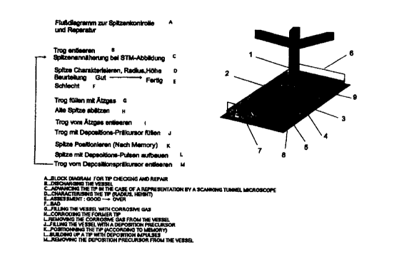
Fig. 7 shows a flow chart of the working stages for the
characterization of microtips and for the repair of a write-
read-erase head of an information storage device that works on
the basis of the process according to the invention.
AMENDED PAGE
CA 02299374 2000-02-04
P97131W0.1P
3 shows arrangements ~~or ~~~~
for changing the media in order to carry out~'the
process according to the invention with a inning
probe microscope ',
Fig. 4 shows an arrangement having a plurality of
microtips and a test tip for carryin out the process
during deposition or etching on lar er structure fields
and for three-dimensional construction of
nanostructures, ,~
Fig. 5 shows an arrange nt for regulating the level
and for changing the dia in order to carry out the
process according t the invention when etching with a
scanning probe mi~'oscope,
Fig. 6 shows he working arrangement for in-situ repair
of a micro p of a scanning probe microscope,
Fig. 7 hows a flow chart of the working stages for the
char terization of microtips and for the repair of a
wri e-read-erase head of an information storage device
t t works on the basis of the process according to t:-~e
The working arrangement, shown in Fig. 1, of a
conventional scanning tunneling microscope that is
operated at atmospheric pressure, has a probe 1 which
can be moved in the x, y and z directions by three
piezo motors and which, on its lower end, carries one
or more cantilevers 2 with one or more microtips with
which it is possible to scan a substrate 3 held on a
substrate holder 4. The substrate holder 4 is fastened
on the x-y table 5 that can move in the x-y direction.
_
A scanning tunneling microscope of this type is
controlled by signal electronics (not shown in the
drawing) with an image memory, and image reproduction
and processing systems as well as with a tip movement
CA 02299374 2000-02-04
P97131WO.1P
system and a sample movement system. The electronics
additionally have one or more channels with which the
micratips can be guided in accordance with a
computer-generated pattern and, for imaging, coating or
etching the substrate, various constant or time-varying
and pulsed voltages with amplitude and duration
tailored to the process can be applied to the various
microtips.
In the working arrangement, represented in Fig. 2, for
carrying out the process according to the invention,
the substrate 3 is located on a substrate holder 4 in a
trough 6 that is fastened on the x-y table 5 of a
scanning probe microscope. Dimethylgold
acetylacetonate, which consists of heavy organometallic
molecules with a molecular weight of 380 and has a low
vapor pressure of 40 mtorr is introduced into the
trough 6 at atmospheric pressure as the medium 7. The
heavy vapor 9 of the medium 7 which forms therefore
displaces the air (molecular weight Oz=32) at the
bottom of the trough 6 and, in the course of time,
coats the bottom of the trough 6 to a depth 8 at which
a few monolayers of the vapor 9 cover the substrate 3.
The microtip of the cantilever 2 dips into this layer
over the substrate 3 and water ions are emitted by it.
Through the impact of the ions, the vapor molecules
adsborbed on the surface of the substrate 3 are broken
up and, in the case of deposition, a lasting deposit is
formed on the substrate 3.
In the case of etching, an etching product is created
which, through corresponding selection of an etching
vapor component, is as gaseous as possible so that it
can be transported away by means of vapor movement.
_
For process control, it may be advantageous to bring
the substrate 3 and the medium 7 to the same
temperature or different temperatures. This may
advantageously be done using heating elements under the
CA 02299374 2000-02-04
P97131WO.1P
substrate 3 and with a separately arranged medium
reservoir.
In order to determine the endpoints of the complete
vapor exchange, level measurement of the vapor level is
advantageously used. According to Fig. 3, the level
measurement can be carried out:
- by measuring the thermal conductivity at miniaturized
resistors 15 of a Wheatstone measuring bridge circuit
16 which are fitted at various heights to the inside of
the trough 6, or
- with greater precision, by means of a light source 10
with use of total reflection at the transition to the
denser medium, or
- by evaluating two-beam interference.
Two-beam interference occurs when the light beam 11
emitted by a light source 10 is partially reflected
from the vapor layer and partially penetrates the vapor
layer, and is then reflected from the lower edge of the
vapor layer, that is to say from the bottom of the
trough 6 or from the substrate 3, and on emerging
interferes with the light beam reflected from the
surface. The interference pattern is created by
superposition of the light beams 12, for example with
the aid of a lens 14, on a detector, 13 or screen
placed in its focal plane. From the intensity profile
of the interference pattern, information can then be
derived about the layer thickness of the vapor layer.
In the case of measuring by total reflection and in the
case of evaluating the interference intensity, a line
camera with computer read-out-is advantageously used as
a spatially resolving detector 13.
In order to accelerate the vapor delivery process, it
is advantageous - as represented in Figure 3 - to
CA 02299374 2000-02-04
' 9 - P97131WO.1P
provide at least one reservoir 19 for the medium on the
trough 6. For this purpose, a compensating vapor
quantity 20 is fed to or from the trough 6 through a
tube 17 and a valve 18, by means of a piston 21 which
is actuated in a cylinder 23 by a positioning motor 22.
In this case, the valve setting, the piston position
and the temperature of the substrate 3 may
advantageously be adjusted using computer control.
Using this device, or a similar compensating-volume
control system, which according to Fig. 3 is
constructed- using a bellows 24 and a positioning motor
22, the vapor for the deposition or for the etching can
be controlled and can be taken away and supplied
rapidly, and it is also possible to change from one
medium 7 to others.
In the arrangement represented in Fig. 4 for carrying
out the process on larger structure fields and for
three-dimensional construction of nanostructur~s, a
plurality of microtips 29 that can be addressed
independently via separate conductor tracks 30 are
used. This allows separate driving, for example, in
order to achieve two-dimensional pointwise structured
application 31 and etching in writefields, on a
substrate 28 with simultaneous guiding by a micratip 26
which is driven in read mode using a conductor tack 25
and with which, for example, a predetermined trace 27
is followed by real-time signal evaluation and position
correction.
When using a, for example, square tip array with 100
separately addressable and readable microtips 29, which
are arranged with a fixed or variable grid dimension,
deposits structured in one position can thereby be
produced simultaneously.
In order to fabricate such microtips using the process
of nanolithography with deposition in a particle-beam
instrument, separately addressable microtips with
CA 02299374 2000-02-04
- 10 - P97131WO.1P
100 nm spacing may be constructed in a line array and
even in a square array. Since the ion-emitting
microtips are formed by the Taylor cone of water at the
end of the tip which is presented, the microtips that
are presented establish only the location of the
deposition by their position. By setting the voltage it
is possible, even with microtips that are the same
voltage, for the pattern of the distribution of the
microtips that are present to be deposited with their
spacings and to be reproduced. It may sometimes be
necessary, -for each microtip, to build a resistor that
limits the emission current into the base of the
microtip in order to make it possible for all the
microtips to emit ions uniformly at the same voltage.
A tip array fabricated in this way can advantageously
be used for the preparation of photonic crystals and
further lattice-like structures, such as
computer-generated holograms.
For the storage of information, the fundamental
frequency of the cantilever, at 10 kHz, signifies a
possible read rate of 1 Mbit/s. If one information unit
is deposited in 0.1 ms, then this is also the write
rate of the arrangement. 1 ms is at present required
for the deposition time. A write rate of 100 Kbit/s can
therefore be achieved for the storage of information.
Using the process according to the invention, it is
also possible to remove material by means of etching.
This is advantageous for cleaning the substrate
surfaces and microtips that are to be coated, as well
as for removing materials already deposited. For
example, by virtue of the fluorine contained,
xenondifluoride etches silicon under ion excitation and
produces gaseous etching products.
An arrangement which is suitable for etching and is
operated at atmospheric pressure is represented in
CA 02299374 2000-02-04
- 11 - P97131WO.1P
Fig. 5. As a result of a corresponding gas-vapor supply
and the use of a further trough 32, Which is connected
to the trough 6 of the scanning probe microscope via a
flexible connecting tube 33 and can be adjusted
relative to it in the indicated direction of motion 35,
the etching gas flows through the connector tube,
depending on the difference in level between the trough
6 and the trough 32, and thus moves the vapor
surrounding the microtip. The etching products are
thereby moved away from the microtip. Through the
connected compensating piston 34, with reservoir and
valve, the etching-gas components can be supplied or
removed, in order for the etching process to be
terminated and to be carried out with computer control.
With this arrangement, which is equipped with means
(not represented in the drawing) for level measurement
and which can be operated with computer control, it is
possible to achieve mass transport of the reaction
products by vapor flow during the etching of the
substrate or the microtips. Besides the aforementioned
xenonaifluoride vapor, those solid etchants which have
a high vapor pressure and contain heavy atoms are also
suitable as the etchant.
The working arrangement represented in Fig. 6 for
in-situ repair of a microtip of a scanning probe
microscope shows a presented microtip 39 connected by
means of a conductor track 38. The conductor track 38
is located on a substrate holder 36. The microtip 39 is
surrounded by a high-impedance approach deposit 37
which makes it possible to order the highest point~of
the microtip 39. In order to produce a new microtip, a
working tip 40 is brought to rest over this point and a
tip 41 is put on the working tip 40 using a short
pulse. Using this new tip 41, the microtip 39 is then
re-scanned and the process is repeated with a change in
the pulse length, the voltage, the vapor pressure and
the vapor composition by changing the partial pressure
CA 02299374 2000-02-04
' - 12 - P97131WO.1P
and the material composition of the medium until the
desired fine or coarse tip radius has been produced on
the tip 41.
The process according to the invention can also be used
to store information by depositing molecules and
molecular clusters and for erasing information by
removing or restructuring molecules by means of a
single microtip or by means of a multitip arrangement.
The microtips are in this case guided locally by an
additional -test tip. Reading takes place using the same
microtip, but at a voltage below the reaction threshold
for writing or erasing. The microtip arrangement for
multitip write, read and erase technology can in this
case be produced internally by deposition lithography.
Further, with this process the write-read-erase head
can be repaired in situ, and in order to sustain the
performance of the write-read-erase memory device, it
can be routinely tested and repaired in preprogrammed
fashion.
The flow chart for the automatic procedure of
characterization and repairing for a write-read-erase
head on a data storage device, which works on the basis
of the process according to invention, is reproduced in
Fig. 7.