Note: Descriptions are shown in the official language in which they were submitted.
CA 02299567 2000-02-24
1
SPECIFICATION
TITLE OF THE INVENTION
Data Processor and Data Processing System
FIELD OF THE INVENTION
The present invention relates to a vector processor
and a vector processing system for processing vector data
that are one-dimensionally sequenced.
BACKGROUND OF THE INVENTION
A large number of scientific and technical
computation processes consist mostly of what is known as
vector processing, i.e., execution of the same arithmetic
operation on each of a series of elements making up vector
data. Supercomputers designed to address such scientific
and technical computations have a vector processor that
executes vector processing at high speed on a pipeline
basis using dedicated hardware facilities. Vector
processors are basically structured to comprise: a vector
register for accommodating a plurality of elements
constituting vector data; a vector loading function for
successively loading a series of vector data elements from
memory into the vector register in response to a vector
CA 02299567 2000-02-24
2
load instruction; a vector storing function for
successively storing a series of vector data elements from
the vector register into memory in response to a vector
store instruction; and a vector computing function for
executing the same arithmetic operation on each of a series
of vector data elements in the vector register in response
to a vector operation instruction. Using these functions,
the vector processor rapidly loads, operates on, and stores
vector data on a pipeline basis.
The vector processor further includes what is known
as a chaining function that executes two vector operation
instructions in parallel, one instruction triggering an
operation on the result of another instruction, whereby the
speed of vector processing is improved. Chaining signifies
that if the result of the operation by a given vector
operation instruction serves as data on which the next
vector operation instruction operates, then the next
instruction is carried out immediately after acquisition of
the result of the operation by the current instruction
without waiting for completion of the current instruction,
whereby operations on the elements of vector data are
executed successively. One disadvantage of the chaining
function is that because the time to execute the ensuing
instruction is determined only after the result of the
CA 02299567 2000-02-24
3
operation by the current instruction has been obtained, the
function can only be utilized where the successive
acquisition of the results of the preceding instructions is
guaranteed. In other words, the chaining function is not
applicable to vector load instructions involving memory
access operations in which the data read-out timing is
unpredictable.
A new chaining scheme has been proposed which judges
the time to execute the next instruction for each of vector
data elements for dynamic chaining in order to resolve the
bottleneck of the chaining function and boost the speed of
vector processing. Dynamic chaining involves using
pointers or flags to indicate successively and explicitly
up to which vector data element a vector loading action or
a vector operation has been completed during execution of a
vector load instruction or a vector operation instruction.
The pointers or flags are referenced to determine when to
execute the next vector operation instruction or vector
store instruction for each vector data element in a dynamic
execution setup. The scheme is supposed to permit chaining
even if load delays occur arbitrarily during execution of a
vector load instruction as a result of memory access
contention or the like, whereby the speed of vector
processing is improved. Apparatuses operating under this
CA 02299567 2000-02-24
4
scheme are disclosed illustratively by JPA 6-2310945 and
JPA 8-202687.
SUMMARY OF THE INVENTION
It is therefore an object of the present invention
to provide a vector data processor and a vector processing
system whereby a processing stop time caused by load delays
is minimized during dynamic chaining of vector processing
instructions so as to increase the speed of vector
processing.
The above object may be achieved according to one
aspect of the present invention, which provides a data
processing system comprising either a data processor and a
memory part; or a data processor, a switching part and a
memory part. These components of the system offer features
outlined below, and the object may be accomplished by
implementing any one or a combination of these features.
To carry out high-speed data processing, the data
processor employs a register that has areas for
accommodating a plurality of data elements, and areas for
indicating whether each of the accommodating areas is
filled with data. The data processor also includes a data
input part that outputs address information for reading
data to be set to the register are read in. The address
CA 02299567 2000-02-24
information at least includes memory addresses,
identification information for identifying individual data
elements, identification information for identifying a
data-originating processor, or like information
representing these specifics.
The data processor further comprises a controlling
part which retrieves from the register those data to be
operated on and which sends the retrieved data to an
arithmetic operation part in accordance with an operation
instruction and with the information held in the register,
in order to operate on the desired data loaded in the
register.
The data processor further comprises a register that
has areas for accommodating a plurality of data elements,
and areas for indicating whether the data element in each
of the accommodating areas is the result of an operation.
Also included in the data processor is a data output part
which reads the result of an operation from the register
based on information held in the register and which outputs
the result together with address information.
A switching part (arbitration part) of the data
processor determines when to transfer address information
based on memory status and on address information from the
processor for efficient access execution between at least
CA 02299567 2000-02-24
6
one processor and at least one memory. Such access is
implemented by transferring the address information in
question to a memory to which such a transfer is found
feasible.
Also included in the data processor are an address
information transfer part and a data transfer part designed
for efficient access execution between a plurality of
processors on the one hand and a plurality of memories on
the other hand. The address information transfer part
transfers address information from a processor to a memory,
and the data transfer part transfer data from a memory to a
processor.
A memory part of the data processor outputs
information indicating whether a given memory can accept
access information for efficient execution of access to or
from any other configured memory. In outputting data, the
memory part supplements the data with information included
in the access information.
The object above may be achieved according to
another aspect of the present invention, which provides a
data processing system comprising a data processor and a
memory. The data processor outputs return destination
information and an address, and the memory outputs data
retrieved from the designated address as well as the return
CA 02299567 2000-02-24
7
destination information, whereby data processing is carried
out at high speed.
According to a further aspect of the invention,
there is provided a data processing system comprising a
switching part which, connected interposingly between at
least one memory and at least one processor, determines
when to output address information to a memory based on
address information from the processor and on a signal from
the memory. This feature of the system also helps to
improve the efficiency of data processing.
According to an even further aspect of the invention,
there is provided a data processing system comprising a
plurality of vector processors for executing the same
arithmetic operation repeatedly on each of a plurality of
data elements constituting vector data, and a processor for
selecting one of the vector processors if the instruction
to be executed turns out to be a vector processing
instruction, the processor further transferring the vector
processing instruction to the selected vector processor.
The system makes up a distributed processing setup that
enhances processing efficiency.
According to a still further aspect of the invention,
there is provided a data processing system comprising a
plurality of data processors each including a communication
CA 02299567 2000-02-24
8
part for transferring data between data processors, a
memory for storing data, and a processor for computing data
read from the memory. The processor outputs return
destination information together with an address about the
data to be processed. The memory outputs the data
retrieved from the address in question together with the
return destination information. These components
constitute a large-scale data processing system that
functions efficiently.
Other objects, features and advantages of the
invention will become more apparent upon a reading of the
following description and appended drawings.
BRIEF DESCRIPTION OF THE DRAWINGS
Fig. 1 is a detailed block diagram of a vector
register facility and a vector operation unit;
Fig. 2 is a circuit diagram of a read
synchronization circuit in the vector operation unit;
Fig. 3 is a block diagram of a vector loading unit;
Fig. 4 is a block diagram of a vector storing unit;
Fig. 5 is a block diagram of a read synchronization
circuit in the vector storing unit;
Fig. 6 is a block diagram of a memory module;
Fig. 7 is a block diagram of a switching part;
CA 02299567 2000-02-24
9
Fig. 8 is a block diagram of a data processing
system in a first structure;
Fig. 9 is a block diagram of a vector register
facility and a vector operation unit in a second structure;
Fig. 10 is a block diagram of a vector register
facility and a vector operation unit in a third structure;
Fig. 11 is a block diagram of a read synchronization
circuit in the vector operation unit in the third
structure;
Fig. 12 is a block diagram of a vector register
facility and a vector operation unit in a fourth structure;
Fig. 13 is a block diagram of a vector loading unit
in a second structure;
Fig. 14 is a block diagram of a data processing
system in a second structure;
Fig. 15 is a block diagram of a data processing
system in a third structure;
Fig. 16 is a block diagram of a data processing
system in a fourth structure;
Fig. 17 is a block diagram showing a group of data
processing systems;
Fig. 18 is a timing chart of vector processing
performed by a data processing system; and
Fig. 19 is a timing chart of vector processing
CA 02299567 2000-02-24
1
carried out by a conventional vector processing system.
DESCRIPTION OF THE PREFERRED EMBODIMENTS
Preferred embodiments of this invention will now be
described with reference to the accompanying drawings.
Fig. 8 is a block diagram showing the first
structure of a data processing system embodying the
invention.
The data processing system comprises: a scalar
processing part 6 for decoding program instructions and
executing scalar instructions; a vector processing part 1
for carrying out vector processing; a memory part 8 for
storing data; and a switching part 7 for connecting the
scalar processing part 6 and vector processing part 1 to
the memory part 8. For this embodiment, a set of data
elements constituting a vector will be described as vector
data hereunder. The scalar processing part 6, vector
processing part 1, memory part 8 and switching part 7 may
be constituted individually by multiple semiconductor
integrated circuits, or may be implemented collectively by
a single semiconductor integrated circuit. The number of
signal lines for transferring data in the single chip setup
is allowed to be greater than in the multiple chip
arrangement. Furthermore, the single chip setup eliminates
CA 02299567 2000-02-24
1 1
the need for drivers required conventionally for data
transfer between chips, so that it constitutes a data
processing system operating more efficiently and at higher
speeds than the multiple chip arrangement.
If the scalar processing part 6 and vector
processing part 1 are made of a single semiconductor
integrated circuit, or if the scaler processing part 6,
vector processing part 1 and switching part 7 are
constituted by a single semiconductor integrated circuit,
it is possible to modify the structure of the memory part 8
as desired. That is, with the capacity of the memory part
8 changed as needed, the general versatility of the system
is enhanced.
The scalar processing part 6 decodes program
instructions. If the decoded instruction turns out to be a
scalar instruction, the scalar processing part 6 executes
the instruction; if the instruction is found to be a vector
instruction, the scalar processing part 6 transmits the
vector instruction 61 to the vector processing part 1.
The vector processing part 1 comprises: an
instruction decoding circuit 2 for decoding the vector
instruction 61 coming from the scalar processing part 6; an
operation unit 10 for repeating the same operation on each
of a series of vector data elements; a register facility 20
CA 02299567 2000-02-24
12
made of a plurality of registers for temporarily
accommodating vector data to be fed to the operation unit
10, as well as the results of operations performed by the
operation unit 10; vector loading units VLU1 (30) and VLU2
(40) for retrieving vector data from the memory part 8.and
for writing the data to registers in the register facility
20; and a vector storing unit VSU (50) which retrieves
vector data from registers in the register facility 20 and
writes the data to the memory part 8.
Upon receipt of the vector instruction 61 from the
scalar processing part 6, the instruction decoding circuit
2 orders the operation unit 10, register facility 20,
vector loading units VLUl (30) and VLU2 (40), and vector
storing unit VSU (50) to execute the instruction by
decoding its instruction code and operands.
On receiving a command to execute a vector operation
instruction from the instruction decoding circuit 2, the
operation unit 10 reads vector data elements from a
register or registers in the register facility 20 which are
designated by an operand of the vector operation
instruction. The operation unit 10 performs the operation
on each of the vector data elements in pipeline fashion as
designated by the instruction code of the vector operation
instruction, and writes results of the operations to those
CA 02299567 2000-02-24
13
registers in the register facility 20 which are designated
by an operand of the vector operation instruction.
The register facility 20 has a plurality of
registers each capable of holding vector data made of up to
"n" elements. The registers are used temporarily to
accommodate vector data to be operated on as well as vector
data resulting from operations.
On receiving a command to execute a load instruction
from the instruction decoding circuit 2, the vector loading
units VLU1 (30) and VLU2 (40) read vector data from those
areas in the memory part 8 which are designated by operands
of the load instruction, and write the data to those
register in the register facility 20 which are specified by
operands of the load instruction. The load operation
involves transmitting to the memory part 8 a vector data
read request for each of data elements separately, and
writing the retrieved data elements to the registers in the
register facility 20. The operation is repeated on all
vector data elements involved. This embodiment is capable
of having two vector load instructions executed
simultaneously by the two vector loading units VLU1 (30)
and VLU2 (40). Alternatively, the number of vector loading
units may be increased so as to execute a larger number of
vector load instructions concurrently. As another
CA 02299567 2000-02-24
14
alternative, only one vector loading unit may be provided
to execute one vector load instruction at a time on a
reduced circuit scale.
Upon receipt of a command to execute a vector store
instruction from the instruction decoding circuit 2, the
vector storing unit VSU (50) reads vector data from that
register in the register facility 20 which is designated by
an operand of the vector store instruction, and writes the
data back to that area in the memory part 8 which is
specified by an operand of the vector store instruction.
The vector store operation by the storing unit involves
transmitting to the memory part 8 a vector data write
request for each of data elements separately, and writing
the retrieved data elements to the memory part 8. This
embodiment is capable of having one vector store
instruction executed at a time by the vector storing unit
VSU (50). Alternatively, the number of vector storing
units may be increased so as to execute a plurality of
vector store instructions simultaneously.
The memory part 8 uses a plurality of memory modules
(MMO, MM1, ..., N~iJ-1) 80 to implement an interleaving
setup. Each memory module receives independently, a write
request and a read request for memory access. This means
that even as a memory module is being accessed, another
CA 02299567 2000-02-24
memory module is available for access thereto.
The switching part 7 establishes paths of access
ranging from the scalar processing part 6 as well as from
the vector loading units VLUl (30), VLU2 (40) and VSU (50)
of the vector processing part 1 to each of the memory
modules 80 in the memory part 8. Specifically, the
switching part 7 forwards memory access requests 62, 31, 41
and 51 coming from the scalar processing part 6 as well as
from the VLUl (30), VLU2 (40) and VSU (50) in the vector
processing part 1 to the memory modules 80 (81-0, 81-1, 81-
2, ..., 81-j-1) of an access destination, and sends read
data 82-0, 82-l, 82-2, ..., 82-j-1 from the memory modules
80 to the access sources, i.e., the scalar processing part
6 as well as the VLUl (30) and VLU2 (40) in the vector
processing part 1 (63, 32, 42).
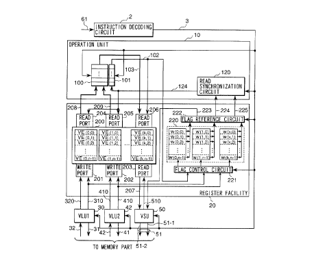
Fig. 1 is a detailed block diagram of the register
facility 20 and operation unit 10 according to the
invention. The register facility 20 has a register file
200 made of a plurality of registers. Each register is
capable of accommodating up to "n" vector data elements.
In Fig. 1, the registers are indicated as VE(i, 0), VE(i,
1), VE(i, 2), ..., VE(i, j), ..., VE(i, n-1). The
indication VE(i, j) stands for a vector data element,
wherein character "i" denotes a register number and "j"
CA 02299567 2000-02-24
16
represents an element number. Vector data element fields
in each register of the register file 200 are each
addressed by use of a register number and an element number
(which constitute an element address). Each register
allows a vector data element to be written independently
thereto through three write ports 201, 202 and 206, and
permits a vector data element to be read independently
therefrom through three read ports 203, 204 and 205.
On receiving a register write command/element
address 310 and data 320 from the vector loading unit VLU1
(30), the write port 201 writes the data to the register
element field designated by the element address. Likewise,
upon receipt of a register write command/element address
410 and data 420 from the vector loading unit VLU2 (40),
the write port 202 writes the data to the register element
field specified by the element address. Similarly, when
receiving a register write command/element address 1020 and
data 103 from the operation unit 10, the write port 206
writes the data to the register element field designated by
the element address.
Upon receipt of a register read command/element
number 124 from the operation unit 10, each of the read
ports 204 and 205 reads data from the register element
field designated by both the element number and the number
CA 02299567 2000-02-24
17
of the register (not shown) subject to the operation
specified by the instruction decoding circuit 2. The
retrieved data 208 and 209 are output to the operation unit
10. When receiving a register read command/element address
510 from the vector storing unit (VSU) 50, the read port
203 reads data from the register element field designated
by the element address. The retrieved data 207 are output
to the vector storing unit (VSU) 50.
The register facility 20 further comprises write
complete flags 220 each indicating that data have been
written to the corresponding register element field, a flag
control circuit 221 for setting and resetting each of the
write complete flags 220, and a flag reference circuit 222
for referencing the set and reset states of each write
complete flag 220.
The write complete flags 220 are each a one-bit flag
corresponding to each of the element fields in each
register. A logical 1 and a logical 0 denote the set and
the reset state of a flag, respectively. In Fig.' 1, each
write complete flag is indicated as W(i, j), where "i"
stands for the register number of the register in question
and "j" for the element number of the corresponding element.
In accordance with a command signal 3 from the
instruction decoding circuit 2, the flag control circuit
CA 02299567 2000-02-24
18
221 resets beforehand the write complete flags 220
corresponding to all elements in the register to which
vector data are to be written upon execution of a vector
instruction. The register may be one into which data are
loaded by a data load instruction, or one to which to write
results of an operation triggered by an operation
instruction. On receiving register write commands/element
addresses 102, 310 and 410 from the operation unit 10,
vector loading unit VLU1 (30) and vector load unit VLU2
(40) respectively, the flag control circuit 221 sets the
write complete flags 220 corresponding to the register
element fields designated by the element addresses in
question. Specifically, when the operation unit 10, vector
loading unit VLU1 (30) and vector load unit VLU2 (40) write
data to certain register element fields in the register
file 200, the flag control circuit 221 sets the write
complete flags 220 corresponding to the register element
fields in question.
In keeping with a command signal 3 from the
instruction decoding circuit 2, the flag reference circuit
222 continuously supplies the operation unit 10 and vector
storing unit (VSU) 50 with values of the write complete
flags 220 corresponding to all elements in registers such
as a register into which data are stored by a vector store
CA 02299567 2000-02-24
19
instruction or a register subject to an operation by a
vector operation instruction. If the vector instruction to
be executed is a vector operation instruction and if a
single register is designated by an operand as subject to
the operation, then the flag reference circuit 222 supplies
the operation unit 10 with write complete flag values 224
of the write complete flags 220 corresponding to all
elements in the register of interest. If the vector
instruction to be executed is an operation instruction and
if two registers are designated by an operand as subject to
the operation, then the flag reference circuit 222 supplies
the operation unit 10 with write complete flag values 224
and 225 of the write complete flags 220 corresponding to
all elements in the two registers. If the vector
instruction to be executed is a store instruction, then the
flag reference circuit 222 supplies the vector storing unit
(VSU) 50 with write complete flag values 223 of the write
complete flags 220 corresponding to all elements of the
registers) in question.
The operation unit 10 comprises: an operation
pipeline 100 for operating on one or two vector data
elements individually on a pipeline basis and for
outputting the results as vector data; a read
synchronization circuit 120 for controlling the supply of
CA 02299567 2000-02-24
vector data from the register facility 20 to the operation
pipeline 100; and a delay circuit 101 which, when the
operation pipeline 100 is fed with a vector data element,
receives the corresponding element address simultaneously,
and outputs the element address at the same time as the
output of the result of the operation after a delay time
required for the operation of the input element address.
The vector operation pipeline 100 is made of one or
a plurality of operation pipelines for carrying out various
operations such as integer operations, floating-point
operations and logic operations. The vector operation
pipeline 100 operates on vector data from the register file
200 and writes the results of the operation to the register
file 200, element by element in a plurality of stages on a
pipeline basis. Operations on two or more vector data
elements (e.g., addition of two vector data elements) are
carried out in such a manner that each of the elements
whose element numbers are identical is operated on
independently. In accordance with the command signal 3
from the instruction decoding circuit 2, the operation
pipeline 100 subjects each of either one or two vector data
elements 208 and 209 from the register file 200 to the
operation designated by the instruction code. Upon elapse
of the number of pipeline stages determined by the
CA 02299567 2000-02-24
21
operation in question, the operation pipeline 100 outputs
the result 103 of the operation with respect to each vector
data element.
In keeping with the command signal 3 from the
instruction decoding circuit 2, the read synchronization
circuit 120 reads vector data in units of elements from the
registers) in the register file 200 which is designated by
an operand, and supplies the retrieved data to the
operation pipeline 100. If a single register is designated
by the operand as subject to the operation, the read
synchronization circuit 120 selects one written data
element at a time from the register by referencing the
write complete flag values 224, and transmits the read
request command and address 124 of the element in question
to the read port 204 of the register facility 20. The
selecting and transmitting actions are repeated until all
data elements have been retrieved. If two registers are
designated by the operand as subject to the operation, the
read synchronization circuit 120 selects one pair of
written data elements at a time from the two registers by
referencing the write complete flag values 224 and 225, and
transmits the register read command/element number 124 of
the elements in question to the read ports 204 and 205 of
the register facility 20. The selecting and transmitting
CA 02299567 2000-02-24
22
actions are also repeated until all data elements have been
retrieved. On receiving the register read command/element
number 124 from the read synchronization circuit 120, the
read ports 204 and 205 read data elements 208 and 209
designated by the element number 124 form inside the
registers specified by the instruction decoding circuit 2,
and feed the retrieved data to the operation pipeline 100.
In this manner, the elements having the same element number
of the vector data subject to the operation are placed
altogether into the register file. When found ready to be
operated on, these data elements are fed successively to
the operation pipeline 100 regardless of the sequence of
their element numbers.
The delay circuit 101 receives the element number
124 sent by the read synchronization circuit 120 to the
read ports 204 and 205 (i.e., element number of the data
element fed to the operation pipeline 100), as well as the
element address made of the register number of an operation
result accommodating destination register (not shown)
designated by the instruction decoding circuit 2. Upon
elapse of a delay time equivalent to what it takes to
perform the operation, the delay circuit 101 outputs the
element number together with a register write command (102).
That is, the operation pipeline 100 outputs the operation
CA 02299567 2000-02-24
23
result 103 while the delay circuit 101 outputs the register
write command 102 and the element address designating the
destination address to which to place the operation result.
Alternatively, the delay time taken by the delay circuit
101 in outputting the element address 102 may be made
shorter than the operation time by as much as a
predetermined period, so that the register write
command/element address 102 may be output earlier than the
operation result. This arrangement has the advantage of
shortening the time required to write the operation result
to the register file 200.
The register facility 20 and operation unit 10 above
have either one or two vector elements fed at a time to the
operation pipeline. Alternatively, a variation of this
embodiment permits execution of vector operations on three
or more vector data elements, such as a product-sum
operation that involves obtaining the product of two vector
data elements and adding the product to a third vector data
element concurrently. To implement such a variation of the
invention requires adding more report ports to the register
file 200 and increasing the number of write complete flag
values output from the flag reference circuit 222 to the
read synchronization circuit 120. In that alternative
setup, the read synchronization circuit 120 may reference
CA 02299567 2000-02-24
24
the write complete flag values of three or more vector
registers subject to the operation in question, and may
output a register read command/element number 124 to three
or more read ports of the register file 200, thereby
causing three or more vector data elements to be fed at a
time to the vector operation pipeline 100.
Fig. 2 is a detailed circuit diagram of the read
synchronization circuit 120 according to the invention.
The read synchronization circuit 120 comprises: an AND
circuit 121 that determines whether each data element has
been written to an element field in the register subject to
the operation and whether each data element has yet to be
read out: an element number selection circuit 122 for
selectively outputting one of the element numbers that have
been written and have yet to be read out; and read complete
flags 123 each indicating that the corresponding data
element is read from the register and supplied to the
operation pipeline 100.
The AND circuit 121 receives the command signal 3
from the instruction decoding circuit 2. If the command
signal 3 is found to designate a single register subject to
the operation, the AND circuit 121 computes for each
element the AND of a write complete flag value 224 with a
logically inverted value 125 of the read complete flag 123
CA 02299567 2000-02-24
and outputs the result. If the command signal 3 is found
to specify two registers subject to the operation, the AND
circuit 121 computes for each element the AND of the write
complete flag values 224 and 225 with the logically
inverted value 125 of the read complete flag 123 and
outputs the result. In this manner, a logical 1 is output
for each of all data elements that are given the same
element number, have been written and have yet to be read
out from each register subject to the operation; otherwise
a logical 0 is output.
The element number selection circuit 122 receives
the output of the AND circuit 121 regarding each data
element. From among all elements whose output values are
1's, i.e., from among all elements that share the same
element number, have been written and have yet to be read
out, the element number selection circuit 122 selects the
element with the smallest element number and outputs the
register read command/element number 124 of the element in
question.
In accordance with the command signal 3 from the
instruction decoding circuit 2, the read complete flags 123
reset as many flags as the number of elements designated by
the instruction as subject to a vector operation starting
from element number 0 prior to the start of the operation;
CA 02299567 2000-02-24
26
the remaining flags are set. Every time the element number
selection circuit 122 outputs a register read
command/element number 124, the read complete flags 123 set
the flag corresponding to the element number in question.
Each element whose reading has been completed is removed
from the candidates for selection by the element number
selection circuit 122. When all elements subject to the
operation have been read out and all read complete flags
123 have been set, the element number selection circuit 122
stops outputting the read request command and element
number 124. The time at which all read complete flags 123
have been set corresponds to the time at which all vector
data in the vector registers subject to the operation have
been fed to the operation pipeline 100. Then the registers
in question are freed, and the vector operation is
terminated upon elapse of the time period required by the
operation since the time at which the registers are freed.
In this respect, the read synchronization circuit 120 may
alternatively notify the instruction decoding circuit 2 or
scalar processing part 6 of the completion of the vector
operation instruction at the time when all read complete
flags 123 have been set or upon elapse of the operation
time since that time.
As described, read synchronization circuit 120 works
CA 02299567 2000-02-24
27
in such a manner that when data elements have been written
to the registers subject to the operation and when the
write complete flags corresponding to all elements sharing
the same element number have been set, these elements are
immediately supplied to the operation pipeline 100. This
means that when the elements sharing the same element
number of the vector data subject to the operation are all
set to the register file and are found ready to be operated
on, these data elements are fed successively to the
operation pipeline 100 regardless of the sequence of their
element numbers.
Fig. 3 is a detailed block diagram of the vector
loading unit VLU1 (30) according to the invention. The
vector loading unit VLU2 (40) has the same structure.
The vector loading unit VLUl (30) comprises: a
memory address buffer (adr) 303 for holding the starting
address of a load source memory; a stride value buffer
(std) 304 for accommodating a stride value; an element
count buffer (num) 305 for retaining the number of
elements; a register number buffer (reg) 306 for storing
the register number of a load destination vector register;
a memory read control circuit 302 for controlling a data
read operation on memory; a register write control circuit
301 for controlling a data write operation on registers; a
CA 02299567 2000-02-24
28
data buffer 308 for temporarily accommodating data read
from memory; and an element number buffer 307 for
temporarily retaining the element number of a load
destination element for the data in question.
The vector loading unit VLU1 (30) executes a vector
load instruction in accordance with the command signal 3
from the instruction decoding circuit 2. As designated by
the command signal 3, the vector loading unit VLUl (30)
sets to the memory address buffer 303 the starting address
in memory at which the vector data to be loaded are held,
and writes the designated stride value, element count and
load destination register number to the stride value buffer
304, element count buffer 305 and register number buffer
306 respectively, before starting the memory read control
circuit 302.
The memory read control circuit 302 reads vector
from memory in units of elements. In operation, the memory
read control circuit 302 first outputs a memory read
command 31 designating the starting address of vector data
as the read address, then outputs a memory read command 31
in which the sum of the read address and the value in the
stride value buffer 304 is designated as the read address,
and further outputs a memory read command 31 in which the
sum of the read address and the value of the stride value
CA 02299567 2000-02-24
29
buffer 304 is designated as the read address. The
operations above are repeated by the memory read control
circuit 302 as many times as the value set in the element
count buffer 305 to request the reading of the applicable
vector data elements from the memory. In addition, the
memory read control circuit 302 supplements the memory read
commands, as they are output, with serial numbers 0, 1, 2,
etc., and regards the added numbers as write destination
element numbers for the read data corresponding to the
memory read commands. Furthermore, the memory read control
circuit 302 supplements each memory read command with an
identical access source number explicitly indicating that
the memory read request source is the vector loading unit
VLUl (30). On receiving such a memory read command, the
memory reads the data designated by the read address and
supplements the retrieved data with the element number and
access source number of the memory read command before
returning the data to the vector loading unit VLU1 (30).
The memory read control circuit 302 checks the received
read data 32 for the access source number. If the checked
data are found to be the read data corresponding to the
memory read command issued by this memory read control
circuit 302, this circuit 302 writes the data and the
element number to the data buffer 308 and element number
CA 02299567 2000-02-24
buffer 307 respectively, and transmits a data reception
signal 309 to the register write control circuit 301
specifying that the read data be written to the appropriate
register.
The register write control circuit 301 writes vector
data read from the memory to registers in the register file
200 in units of data elements. On receiving a data
reception signal 309 from the memory read control circuit
302, the register write control circuit 301 outputs a
register write command 310 that contains a load destination
register number indicated by the register number buffer 306
and an element number held by the element number buffer 307
as an element address. At the same time, the register
write control circuit 301 outputs the data 320 placed in
the data buffer 308 to the write port 201 of the register
file 200.
As described, in the loading unit VLU1 (30) when
vector data are to be read from the memory in units of
elements, the memory read commands involved are
supplemented with the applicable element numbers before
being sent to the memory. Each data element retrieved from
the memory is returned together with the corresponding
element number to the loading unit VLU1 (30). In this
manner, even if the sequence of memory read requests from
CA 02299567 2000-02-24
31
the vector loading unit VLUl (30) does not match the
sequence of read data returned by the memory, the vector
loading unit VLU1 (30) can write the read data returned by
the memory to the correct element numbers in the registers.
Fig. 4 is a detailed block diagram of the vector
storing unit VSU (50) according to the invention. The
vector storing unit VSU (50) comprises: a memory address
buffer (adr) 503 for holding the starting address of a
store destination memory; a stride value buffer (std) 504
for accommodating a stride value; an element count buffer
(num) 505 for retaining the number of elements; a register
number buffer (reg) 506 for storing the register number of
a store source vector register; a memory write control
circuit 502 for controlling a data write operation on
memory; a register read control circuit 501 for controlling
a data read operation on registers; a read synchronization
circuit 520; and a data buffer 508 for temporarily
accommodating data read from registers.
The vector storing unit VSU (50) executes a vector
store instruction in accordance with the command signal 3
from the instruction decoding circuit 2. As designated by
the command signal 3, the vector storing unit VSU (50) sets
to the memory address buffer 503 the starting address in
memory to which to store the vector data, and writes the
CA 02299567 2000-02-24
32
designated stride value, element count and store source
register number to the stride value buffer 504, element
count buffer 505 and register number buffer 506
respectively, before starting the memory write control
circuit 502.
The read synchronization circuit 520 is
substantially the same in structure as the read
synchronization circuit 120 of the operation pipeline 100
described with reference to Fig. 2. The only difference
between the two circuits is that unlike the read
synchronization circuit 120, the circuit 520 refers to the
write complete flags of a single register alone, as shown
in Fig. 5.
Before the start of a vector store operation, the
read synchronization circuit 520 resets as many flags as
the number of data elements designated by the instruction
as subject to the operation starting from element number 0
of read complete flags 523, and sets the remaining flags.
The read synchronization circuit 520 then selects one of
the elements that have been written and have yet to be read
out, by getting an element number selection circuit 522 to
reference the write complete flag values 223 and read
complete flags 523. The selected element number 524 is
output to the register read control circuit 501, and the
CA 02299567 2000-02-24
33
read complete flag 523 corresponding to the element number
in question is set. Each element whose reading has been
completed is removed from the candidates for selection by
the element number selection circuit 522. When all
elements subject to the operation have been read out and
all read complete flags 523 have been set, the element
number selection circuit 522 stops outputting the read
request command and element number 524. The time at which
all read complete flags 523 have been set corresponds to
the time at which all register data subject to the store
operation have been fed to the vector storing unit VSU (50).
Then the registers in question are freed. In this respect,
the read synchronization circuit 520 may alternatively
notify the instruction decoding circuit 2 or scalar
processing part 6 (not shown) of the completion of
execution of the vector store instruction at the time when
all read complete flags 523 have been set or upon elapse of
the operation time since that time.
In response to the element number 524 output by the
read synchronization circuit 520, the register read control
circuit 501 reads out the corresponding data element from
the designated register. On receiving the element number
524 from the read synchronization circuit 520, the register
read control circuit 501 outputs to the read port 203 of
CA 02299567 2000-02-24
34
the register file 200 the value of the register number
buffer 506, i.e., the element address formed by the number
of the register subject to the store operation and by the
element number 524, as well as a register read command 510.
The register read control circuit 501 sets to the data
buffer 508 the data returned from the read port 203, and
transmits a data reception signal 509 to the memory write
control circuit 502 to notify the latter of data reception.
The memory write control circuit 502 writes vector
data to memory in units of data elements. On receiving a
first data reception signal 509 from the register read
control circuit 501, the memory write control circuit 502
outputs the value of the memory address buffer 503, i.e., a
memory write command 51-1 designating the starting address
of vector data as the write address, as well as data 51-2
held in the data buffer 508. Upon receipt of a second data
reception signal 509, the memory write control circuit 502
outputs a memory write command 51-1 designating the write
address as the sum of the write address from the preceding
operation and the value of the stride value buffer 504, as
well as the data 51-2 held in the data buffer 508. When
receiving a third data reception signal 509, the memory
write control circuit 502 outputs a memory write command
51-1 designating the write address as the sum of the write
CA 02299567 2000-02-24
address from the preceding operation and the value of the
stride value buffer 504, as well as the data 51-2 retained
in the data buffer 508. The operations above are repeated
as many times as the value in the element count buffer 505
to request the writing of the vector data elements to the
memory. As described, when the vector storing unit VSU
(50) reads vector data in units of elements from the
register subject to a store operation to memory, the read
synchronization circuit 520 checks the write complete flags
corresponding to the elements in question. Every time a
write complete flag is found to be set, the applicable
element is immediately read from the register and stored
into the memory. In this setup, whenever the operation
pipeline 100 of the operation unit 10 writes results of
operations to registers in units of data elements, these
results are stored without delay into the memory regardless
of the sequence of the element numbers involved.
Fig. 6 is a detailed block diagram of one of memory
modules ( N~IO , MM1 , . . . ,
MMJ-1) 80 in the memory part 8
according to the invention.
A memory module 80 comprises: an access request
buffer 802 for accommodating one or a plurality of sets 81-
0 of a memory read/write command, an access destination
address, write data, an element number, and an access
CA 02299567 2000-02-24
36
source number received from the switching part 7; an access
return buffer 805 for holding one or a plurality of sets of
read data, an element number, and an access source number;
one or a plurality of memory banks 801; a bank control
circuit 803 for controlling access to the memory banks; and
a data return control circuit 804 for controlling the
return of read data.
Each memory mode 80 temporarily retains in its
access request buffer 802 a memory read/write command
together with an access destination address 8021, an
element number together with an access source number 8022,
and write data 8023 received from the switching part 7,
until the access in question is terminated. When the
number of free fields in the access request buffer 802 has
dropped below a predetermined count, the memory module 80
outputs a busy signal 806 to the switching part 7 until the
free field count in the buffer exceeds the predetermined
value.
Each memory bank 801 is capable of executing only
one memory access operation at a time. An attempt to
perform a plurality of memory access operations on a single
memory bank leads to successively executing the access
operations involved. On the other hand, a plurality of
memory access operations may be performed simultaneously on
CA 02299567 2000-02-24
37
different memory banks. From among the memory access
requests held in the access request buffer 802, the bank
control circuit 803 selects one that corresponds to a
memory bank 801 on which a memory access operation has yet
to be carried out; and sends to that bank a memory
read/write command and an access destination address 8031,
as well as write data 8033 if the access involved is a
write operation. Selection of the memory access requests
is not restricted by the sequence in which these requests
were placed into the access request buffer 802. However,
if there exist a plurality of memory access requests that
may be selected, it is preferred to select them in the
order in which they were placed into the buffer. If a
memory access request calls for a read access operation,
there must be free space in the access return buffer 805
before the operation can take place. Before execution of
such a read access operation, one free field should be
secured in the access return buffer 805. The read data
8011 read from the memory bank 801 are placed into that
access return buffer 805, and the read access element
number and access source number 8032 held in the access
request buffer 802 are also set to the access return buffer
805.
The data return control circuit 804 adds the element
CA 02299567 2000-02-24
38
number and the access source number to the read data in the
access return buffer 805 before outputting the data (82-0).
Basically, the data return control circuit 804 returns the
read data in the order in which the data were placed into
the access return buffer 805. Alternatively, the data
return control circuit 804 may have a status signal line
interposed between the circuit and each of return
destination units, the line carrying a status signal
indicating whether the return destination unit in question
can receive the returned data. The data may then be
returned preferentially to any unit judged ready to receive
them in accordance with the signal on the status signal
line.
Fig. 7 is a detailed block diagram of the switching
part 7 according to the invention. The switching part 7
has two major components: an access request transfer unit
71 for transferring memory access requests output by the
scalar processing part 6 and vector processing part 1 to
access destination memory modules 80 in the memory part 8;
and a read data transfer unit 75 for transferring read data
output by the memory modules 80 in the memory part 8 to the
scalar processing part 6 and vector processing part 1 which
are return destinations.
The access request transfer unit 71 comprises:
CA 02299567 2000-02-24
39
access request buffers 713, 714, 715 and 716 each
accommodating one or a plurality of sets 62, 31, 41 and 51
of a memory read/write command, an access destination
address, write data, an element number, and an access
source number received from the scalar processing part 6 as
well as the vector loading unit VLU1 (30), vector loading
unit VLU2 (40) and vector storing unit VSU (50) of the
vector processing part 1; a crossbar switch 711 for
constituting transfer paths; and an arbitration circuit 710
for controlling the crossbar switch 711.
The crossbar switch 711 has four inputs and J
outputs (J = number of memory modules in the memory part 8)
which provide connections between desired inputs and
outputs. The inputs and outputs of the switch are each
capable of transferring all of the memory read/write
command, access destination address, write data, element
number, and access source number of each access request.
Preferably, the number of signal lines may be reduced by
having a signal line for write data double as a signal line
for element numbers and access source numbers. Over the
shared signal line, write data may be transmitted upon
transfer of a memory write command, and an element number
and an access source number may be transmitted upon
transfer of a memory read command.
CA 02299567 2000-02-24
The arbitration circuit 710 checks the access
destination addresses of access requests in the access
request buffers 713, 714, 715 and 716, as well as the busy
signal 806 of each memory module. If a given access
request has no other contending access request for the same
memory module and if that memory module is not outputting a
busy signal 806, the arbitration circuit 710 immediately
causes the crossbar switch 711 to form a transfer path
through which the access request in question is transferred
to the access destination memory module. If a given access
request has any contending access request for the same
memory module and if that memory module is not outputting a
busy signal 806, the arbitration circuit 710 selects one of
the contending access requests in accordance with
predetermined arbitration conditions and causes the
crossbar switch 711 to form a transfer path through which
the selected access request is transferred to the access
destination memory module.
The read data transfer unit 75 is structurally
similar to the access request transfer unit 71. The read
data transfer unit 75 comprises: access return buffers 753-
0, 753-1, 753-2, ..., 753-j-1 each accommodating one or a
plurality of sets 82-0, 82-1, 82-2, ..., 82-j-1 of read
data, an element number, and an access source number
CA 02299567 2000-02-24
41
received from the memory modules 80 in the memory part 8; a
crossbar switch 751 for constituting transfer paths; and an
arbitration circuit 750 for controlling the crossbar switch
751. The crossbar switch 751 has J inputs and four outputs
(J = number of memory modules in the memory part 8) which
provide connections between desired inputs and outputs.
The inputs and outputs of the switch are each capable of
transferring all of the read data, element number and
access source number.
The arbitration circuit 750 checks the access source
numbers of the read data in the access return buffers 753-0,
753-l, 753-2, ..., 753-j-1. If a given read data element
has no other contending read data element to be returned to
the same access source, the arbitration circuit 750
immediately causes the crossbar switch 751 to form a
transfer path through which the read data element in
question is transferred to the access source, i.e., the
scalar processing part 6, or one of the vector loading
units VLU1 (30) and VLU2 (40) of the vector processing part
1. If a given read data element has any contending read
data element to be returned to the same access source, the
arbitration circuit 750 selects one of the contending read
data elements according to predetermined arbitration
conditions and causes the crossbar switch 751 to form a
CA 02299567 2000-02-24
42
transfer path through which the selected read data element
is transferred to the access source, i.e., the scalar
processing part 6, or one of the vector loading units VLU1
(30) and VLU2 (40) of the vector processing part 1.
As described, the switching part 7 allows the access
request transfer unit 71 and read data transfer unit 75
independently to handle the transmission of access requests
to the memory part 8 and the returning of read data from
the memory part 8. There is no interference between access
request transfers and read data returned. Furthermore, the
access request transfer unit 71 and read data transfer unit
75 are each capable of permitting simultaneous access
operations between the access sources (scalar processing
part 6 as well as vector loading units VLU1 (30) and VLU2
(40) of the vector processing part 1) on the one hand and
the access destinations (a plurality of memory modules in
the memory part 8) on the other hand, provided that access
sources and destinations are different from one another.
This feature provides more efficient access to the memory
than before.
If the memory part 8 and switching part 7 are formed
in a single semiconductor integrated circuit, it becomes
possible to read data at high speed in response to access
requests from the scalar processing part 6 or vector
CA 02299567 2000-02-24
43
processing part 1. Where a large number of memory modules
80 are provided, the switching part 7 and memory part 8 may
preferably be formed into a single semiconductor integrated
circuit instead of the memory part 8 alone being made into
one semiconductor integrated circuit. This arrangement
having less terminals helps reduce the scale of the circuit.
Fig. 18 is a timing chart of vector processing
performed by a data processing system embodying the
invention.
The vector processing illustrated in Fig. 18
involves first getting the vector loading units VLU1 (30)
and VLU2 (40) to load vector data A and B made of 16
elements each from the memory part 8, causing the operation
unit 10 to operate on the two sets of vector data, and
finally ordering the vector storing unit VSU (50) to store
the results of the operation into the memory part 8. It is
assumed for the timing chart of Fig. 18 that a vector
processing system of a second structure is used. For
purpose of simplification and illustration, it is assumed
that pipeline stages for vector computations are given in
units of four cycles, that eight memory modules are
included in the memory part 8, that there is one bank for
each memory module for a total of eight banks in the memory
part 8, and that it takes four unit cycles to access each
CA 02299567 2000-02-24
44
bank.
Given their respective vector load instructions, the
vector loading units VLU1 (30) and VLU2 (40) output
simultaneously to the memory part 8 data read request
commands for elements 1 through 16 in each unit cycle in
the order of the element numbers involved. Suppose that
the elements of vector data to be loaded by the vector
loading unit VLU1 (30) are held in every second bank
starting from bank 0 in the memory part 8, and that the
elements of vector data to be loaded by the vector loading
unit VLU2 (40) are held in every fourth bank starting from
bank 4 in the memory part 8. In such a case, access
contention is bound to occur in several banks subject to
the data read operations by the two vector loading units.
Illustratively, an attempt to read element 3 of vector data
A from bank 2 conflicts with an attempt to read element 3
of vector data B from the same bank, causing a delay of
four unit cycles in the reading of element 3 of vector data
B. Similarly, an attempt to read element 6 of vector data
A conflicts with an attempt to read element 4 of vector
data B, causing a delay of two unit cycles in the reading
of element 6 of vector data A. These and many other cases
of access contention cause delays in the loading of several
data elements. With this embodiment, however, the vector
CA 02299567 2000-02-24
loading units VLU1 (30) and VLU2 (40) add an access source
number designating the destination to which to return the
read data as well as an element number to each data read
request command before outputting the command to the memory
modules in the memory part 8. In turn, each memory module
supplements the read data with the access source number and
element number before returning the data to the vector
loading units VLU1 (30) and VLU2 (40). The scheme allows
earlier elements delayed due to access contention to be
overtaken by subsequent elements so that the latter will be
loaded earlier. In the above example, element 3 of vector
data B is overtaken by elements 4 and 5 in a load operation,
and element 6 of vector data A overtaken by element 7 in
another load operation. That is, vector data are loaded
efficiently without being constrained by the order of their
element numbers.
The vector loading units VLU1 (30) and VLU2 (40)
were described above as loading to registers the elements
of vector data A and B in a sequence different from that of
the element numbers involved. Likewise, the operation unit
10 will execute vector operations upon completion of the
loading of each data element, i.e., in a sequence different
from that of the element numbers. Every time elements of
vector data A and B are written to registers, the
CA 02299567 2000-02-24
46
corresponding write complete flags are set. By referring
to these flags using the read synchronization circuit 120,
the operation unit 10 supplies the operation pipeline 100
with the elements having the same element number in the two
sets of vector data immediately after the elements have
been written to the registers. At the same time, the
operation unit 10 inputs the data elements to the delay
circuit 101. The operation unit 10 writes the results of
the operation output by the operation pipeline 100 to the
register element numbers output by the delay circuit 101
upon elapse of a predetermined time period. In the above
example, elements 4 of both sets of vector data, loaded
earlier than elements 3 of the two vector data sets in unit
cycle 8, are fed to the operation pipeline 100 in the next
unit cycle 9; elements 3 of both sets of vector data,
subsequently loaded in unit cycle 11, are supplied to the
operation pipeline 100 in the next unit cycle 12; and so on.
In this manner, the vector data elements loaded to the
registers by the vector loading units VLU1 (30) and VLU2
(40) in a sequence different from that of the element
numbers involved are efficiently operated on, free of the
constraints of the element number sequence.
As described, the vector loading units VLU1 (30) and
VLU2 (40) load the elements of vector data A and B into the
CA 02299567 2000-02-24
47
registers efficiently in a sequence different from that of
the element numbers, and the operation unit 10 also carries
out operations on the elements of both sets of vector data
in a sequence different from that of the element numbers.
In like manner, every time an operation on a given element
is completed, the vector storing unit VSU (50) stores the
result of the operation to the memory part 8. That is, the
results of operations on the vector data elements are
stored in a sequence different from that of the element
numbers. Each time results of operations on two elements
of both sets of vector data are written to registers, the
corresponding write complete flags are set. By referring
to these flags using the read synchronization circuit 520,
the vector storing unit VSU (50) stores the results of
operations on given elements into the memory part 8
immediately after the results have been written to the
registers. In this manner, the results of operations
output by the operation pipeline 100 in an order different
form that of the element numbers involved are efficiently
stored into the memory part free of the constraints of the
element number sequence.
As described, the loading, operation and storing of
vector data are performed not only in a chained fashion on
each of vector data elements but also in a sequence
CA 02299567 2000-02-24
48
different from that of the element numbers involved. This
makes it possible to perform a series of vector processes
efficiently regardless of access contention in the memory
part 8. For purpose of comparison with the timing chart of
Fig. 18, Fig. 19 shows a timing chart of vector processing
carried out by a conventional system with comparable
settings. The conventional system carries out the loading,
operation and storing of vector data in the order of the
numbers of elements constituting the vector data.
Comparing the two timing charts indicates that the vector
processing by the conventional system in Fig. 19 has a
process stop time of 12 unit cycles due to memory access
contention, while the processing by the inventive system in
Fig. 18 is subject to a reduced stop time of four unit
cycles.
Fig. 9 is a detailed block diagram of the register
facility 20 and operation unit 10 in the second structure
according to the invention.
The register facility 20 and operation unit 10 in
Fig. 9 are basically the same in structure as their
counterparts in Fig. 1. What makes the components in Fig.
9 distinct is that the operation unit 10 has two operation
pipelines 100-1 and 100-2 associated respectively with
delay circuits 101-1 and 101-2 and with read
CA 02299567 2000-02-24
49
synchronization circuits 120-1 and 120-2, and that the
register file 200 of the register facility 20 has read
ports 204-1 and 205-1 and a write port 206-1 connected to
the operation pipeline 100-1, as well as read ports 204-2
and 205-2 and a write port 206-2 linked to the operation
pipeline 100-2. Because the operation units 10-1 and 10-2
of the structure in Fig. 9 are capable of performing vector
operations independently of each other, two vector
operation instructions can be executed simultaneously.
Furthermore, it is possible to perform a given vector
operation followed immediately by another vector operation
that is carried out on the result of the preceding
operation in a chained, parallel fashion. Although this
structure has two vector operation pipelines in the
operation unit 10, this is not limitative of the invention.
Alternatively, three or more vector operation pipelines may
be provided so as to execute three or more vector operation
instructions simultaneously.
Fig. 10 is a detailed block diagram of the register
facility 20 and operation unit 10 in the third structure
according to the invention.
The register facility 20 and operation unit 10 in
Fig. 10 are basically the same in structure as their
counterparts in Fig. 1. What makes the components in Fig.
CA 02299567 2000-02-24
10 distinct is that the operation unit 10 has two operation
pipelines 100-1 and 100-2 associated respectively with
delay circuits 101-1 and 101-2, as well as a read
synchronization circuits 120-3 for controlling the supply
of data to the two operation pipelines, and that the
register file 200 of the register facility 20 has read
ports 204-1 and 205-1 and a write port 206-1 connected to
the operation pipeline 100-1, as well as read ports 204-2
and 205-2 and a write port 206-2 linked to the operation
pipeline 100-2. The operation units 10-1 and 10-2 are
capable of executing the same vector operation, and the
read synchronization circuit 120-3 distributes elements of
vector data subject to a given operation to the two
operation pipelines. This scheme allows the operation unit
10 of Fig. 10 to process two data elements in a single unit
time whereas the vector operation unit 10 in Fig. 1
processes one element in the same unit time. That is, the
operation unit 10 of Fig. 10 can reduce the execution time
of vector operation instructions by half. Although this
structure has two vector operation pipelines in the
operation unit 10, this is not limitative of the invention.
Alternatively, three or more vector operation pipelines may
be provided to further reduce the execution times of vector
operation instructions.
CA 02299567 2000-02-24
51
Fig. 11 is a block diagram of the read
synchronization circuit 120-3 in the vector operation unit
of Fig. 10.
The read synchronization circuit 120-3 is basically
the same in structure as the read synchronization circuit
120 described in reference to Fig. 2. The difference is
that the read synchronization circuit 120-3 causes an
element number selection circuit 122-3 to output register
read commands and element numbers 124 with respect to two
data elements. The element number selection circuit 122-3
receives outputs by elements of the AND circuit 121. If
there is an element whose output value is 1, i.e., if all
elements sharing the same element number have been written
and if among them is an element whose reading has yet to be
completed, then the element number selection circuit 122-3
outputs the element number 124 of that element together
with a register read command. If there are two or more
elements whose output value is 1 each, the element number
selection circuit 122-3 selects the element with the
smallest element number and another element with the
second-smallest element number, and outputs these element
numbers 124 and 126 together with a register read command
each. This scheme makes it possible to supply operation-
ready vector data elements simultaneously to the vector
CA 02299567 2000-02-24
52
operation pipelines 100-1 and 100-2 in Fig. 10 when the two
operation pipelines execute a single vector operation
instruction.
Fig. 12 is a detailed block diagram of the operation
unit 10 in the fourth structure according to the invention.
The operation unit 10 of Fig. 12 is basically the
same in structure as its counterpart in Fig. 1. The
difference is that the operation unit 10 of Fig. 12
utilizes an FIFO queue 130 instead of the delay circuit 101.
The FIFO queue 130 stores successively the element numbers
124 of data elements which are output by the read
synchronization circuit 120 and fed to the operation
pipeline 100. The queue 130 outputs the element numbers in
the order in which they were stored, in keeping with the
results of operations output by the operation pipeline 100.
In this manner, the FIFO queue 130 can output the element
numbers corresponding to the operation results regardless
of the time required for vector operations. While this
structure substitutes the FIFO queue for the delay circuit
101 in the operation unit 10 of Fig. 1, the delay circuit
of the operation unit 10 in Fig. 9 or 10 may also be
replaced by an FIFO queue each. The replacement also
provides similar advantageous effects.
Fig. 13 is a block diagram of the vector loading
CA 02299567 2000-02-24
53
unit (VLU) 30 in the second structure according to the
invention.
The vector loading unit (VLU) 30 of Fig. 13 is
basically the same in structure as its counterpart in Fig.
3. The difference is that the vector loading unit 30 of
Fig. 13 has an additional element address buffer 330 for
temporarily accommodating element addresses of the register
file 200, each address indicating a load destination to
which to write data retrieved from memory. A plurality of
element addresses may be placed into the element address
buffer 330, and the load location for each element address
is identified by a unique load number. Instead of
supplementing a memory read command 31 with a load
destination element number for output, the memory read
control circuit 302 generates an element address based on
the load destination element number and on the vector
register number of the load destination designated by the
register number buffer 306. The memory read control
circuit 302 places the element address thus generated into
the element address buffer 330, and adds the load number
for the element address to the memory read command 31 for
output. The register write control circuit 301 retrieves
that element address in the element address buffer 330
which is designated by the load number of the received read
CA 02299567 2000-02-24
54
data 32, outputs a register write command 310, and sends
the data 320 from the data buffer 308 to the write port 201
of the register file 200. With this structure, the moment
the memory read control circuit 302 outputs the memory read
command for the last element during execution of a vector
load instruction, it is possible to release the memory
address buffer 303, stride value buffer 304, element count
buffer 305, register number buffer 306 and memory read
control circuit 302 from the load instruction in question.
This allows the next vector load instruction to be executed
without delay. Although not shown, arrangements may be
made so that the instruction decoding circuit 2 or scalar
processing part 6 is notified that execution of the vector
load instruction has been completed as soon as the memory
read control circuit 302 has output the memory read command
for the last element.
Fig. 14 is a block diagram of the data processing
system in the second structure according to the invention.
The data processing system of Fig. 14 is basically
the same in structure as its counterpart in Fig. 1, except
that the switching part 7 is replaced by a memory bus 9 to
reduce the scale of the circuit.
The memory bus 9 comprises: an access signal line 91
for sending access requests from the scalar processing part
CA 02299567 2000-02-24
6 and vector processing part 1 to the memory part 8; a read
data return signal line 92 for returning read data from the
memory part 8 to the scalar processing part 6 or vector
processing part 1; and an access arbitration part 93 for
arbitrating access operations to the memory bus.
The scalar processing part 6 and each of the VLU1
(30), VLU2 (40) and VSU (50) in the vector processing part
1 output access requests onto the access signal line 91
when gaining access to the memory part 8. The access
arbitration part 93 selects one of these access requests in
accordance with predetermined priority criteria to permit
access to the memory by use of the memory bus 9 composed of
a plurality of signal lines. On returning read data to the
scalar processing part 6 or vector processing part 1, the
memory modules 80 in the memory part 8 output return
requests onto the read data return signal line 92. The
access arbitration part 93 selects one of the access and
return requests according to the predetermined priority
criteria to permit access through the memory bus 9.
The structure above permits simultaneous execution
of both the transfer of memory access requests and the
returning of read data over the independently furnished
access signal line 91 and read data return signal line 92,
the access signal line 91 sending access requests from the
CA 02299567 2000-02-24
56
scalar processing part 6 and vector processing part 1 to
the memory part 8, the read data return signal line 92
returning read data from the memory part 8 to the scalar
processing part 6 or vector processing part 1. If memory
access performance permits, the access signal line 91 and
read data return signal line 92 may be formed into a common
line for a further reduction in the scale of the circuit.
The scalar processing part 6, vector processing part
1, access arbitration part 93, and memory part 8 may each
be built in a separate semiconductor integrated circuit.
Alternatively, these components may be integrated into a
single semiconductor integrated circuit to eliminate
drivers and other parts needed to output data. The
alternative structure will make up a high-speed data
processing system on a limited circuit scale.
The scalar processing part 6 and vector processing
part 1 may be formed in a single semiconductor integrated
circuit; or the scalar processing part 6, vector processing
part 1 and access arbitration part 93 may be integrated
into a single semiconductor integrated circuit. Either of
these structures makes it possible to vary the capacity of
the memory part 8 as desired and thereby contributes to
enhancing the general versatility of the system.
Fig. 15 is a block diagram of a data processing
CA 02299567 2000-02-24
57
system in the third structure according to the invention.
This data processing system is formed by having the
memory part 8 of the vector processing system in Fig. 1
made of a hierarchical structure including an internal
memory part 8-1 and an external memory part 8-2, and by
incorporating a scalar processing part 6, a vector
processing part 1 and the internal memory part 8-1 in a
single semiconductor chip or module substrate 1000. The
internal memory part 8-1 and external memory part 8-2 are
structurally the same as the memory part 8, and a switching
part 7-1 for the internal memory part and a switching part
7-2 for the external memory part have the same structure as
that of the switching part 7. A bridge part 1010,
connecting the internal memory switching part 7-1 with the
external memory switching part 7-2, relays access requests
and returned read data between scalar processing part 6 and
vector processing part 1 on the one hand and the external
memory part 8-2 on the other hand. This system permits
access operations from the scalar processing part 6 and
vector processing part 1 to the internal memory switching
part 7-1 inside the chip or module. That is, although
limited to part of the memory, the access operations are
carried out internally and hence at high speed.
Alternatively, the bridge part 1010 may be arranged to have
CA 02299567 2000-02-24
58
a so-called DMA (dynamic memory access) function interposed
between the internal memory part 8-1 and the external
memory part 8-2. In that alternative setup, commands 64
from the scalar processing part trigger consecutive data
transfers between the internal and external memory parts 8-
1 and 8-2.
Fig. 16 is a block diagram of a data processing
system in the fourth structure according to the invention.
This data processing system is basically the same in
structure as its counterpart in Fig. 1 except that a
plurality of vector processing parts are provided. The
multiple vector processing parts 1-1, 1-2, ...,
1-v are
capable of simultaneously processing a plurality of vector
instructions 61-1, 61-2, ..., 61-v sent from the scalar
processing part. The system of Fig. 16 thus permits vector
processing at higher speed than before.
Fig. 17 is a block diagram showing a group of data
processing systems according to the invention.
The group comprises a plurality of data processing
systems (one indicated by 2000) whose structure was
described with reference to Fig. 15, each system being
supplemented with a communication part 2020 having
functions for communicating with the outside. The
plurality of multiple data processing systems 2000, 2100,
CA 02299567 2000-02-24
59
2200 and 2300 having the same structure are interconnected
by a communication network 3000. The communication part
2020 of each data processing system reads data from the
memory part 8 in accordance with a communication
instruction 65 from the scalar processing part to send the
read data to another data processing system, requests
another data processing system to read data from its memory
part in keeping with a communication instruction 65 from
the scalar processing part, or reads data from the memory
part 8 according to a data read request received from
another data processing system to send the read data to the
request source data processing system. When the multiple
data processing systems cooperate to deal with the
processing of data in that manner, vector processing is
accomplished faster than ever before.
As described, the invention provides a data
processing system which, embodied and broadly described
above, is capable of processing operations at high speed.
As many apparently different embodiments of this
invention may be made without departing from the spirit and
scope thereof, it is to be understood that the invention is
not limited to the specific embodiments thereof except as
defined in the appended claims.