Note: Descriptions are shown in the official language in which they were submitted.
CA 02299837 2000-OS-11
TITLE: ELECTRICAL COMPONENT FOR SURFACE-MOUNTING ON A CIRCUIT
BOARD
FIELD OF THE INVENTION
The present invention relates to the field of surface-
mount electrical components. More specifically, it pertains
to a method for mounting and anchoring surface-mount
electrical components, such as electrical connectors, to a
circuit board.
BACKGROUND OF THE INVENTION
With the advancement of circuit board assembly has come
a technique known as surface-mount technology, which consists
in the mounting of electronic circuit components and their
electrical connections on the surface ,of a Printed Circuit
Board (PCB), rather than through holes. The PCB itself is a
flat board whose front contains slots for integrated circuit
chips and connections for a variety of electrical components,
and whose back is printed with electrically conductive
pathways between the components. An example of such an
electrical component is the electrical connector which, when
mounted on the PCB, creates an interface between discrete
wires and the PCB. Automation of the circuit board assembly
process typically involves the use of automated pick-and-
place machinery for placement of the electrical components
onto the PCB.
Existing surface-mount electrical components, such as
the electrical connector, are anchored to the PCB by the
soldering of their electrical pins to the PCB, where these
pins also provide points of electrical contact between the
component and the PCB. However, these components often need
additional means of mechanical fastening in order to restrict
1
CA 02299837 2000-OS-11
the movement of the components on the PCB, as excessive
movement produces undesirable stresses on the electrical pin
solder-joints.
Unfortunately, the anchoring systems currently used to
fasten surface-mount electrical components to circuit boards
have important disadvantages. In the case of metal or
plastic clips, excessively high insertion forces are required
from the pick-and-place machines in an automated assembly,
and access to the opposite side of the PCB may require
drilling of the PCB. In the case of threaded fasteners,
automation of the assembly is rendered very difficult.
The background information herein clearly shows that
there exists a need in the industry to provide an improved
method for anchoring surface-mount electrical components to a
circuit board.
SUMMARY OF THE INVENTION
The invention resides in a novel electrical component
for surface-mounting on a circuit board. The electrical
component includes at least one electrical pin, serving as
both a point of electrical contact between the electrical
component and the circuit board and as a point of solder-
anchoring. The electrical component further includes a novel
anchoring system. The anchoring system comprises a retaining
surface, coplanar with the electrical pin. The retaining
surface is also capable of being solder-anchored to the
circuit board, thus restricting the movement of the
electrical component on the circuit board and eliminating
undesirable stresses on the electrical pin solder-joints.
The electrical component, including the novel anchoring
system, requires zero insertion force to be mounted on the
circuit board. The automation of the surface-mount assembly
2
CA 02299837 2000-OS-11
operation is thus greatly simplified, with no drilling of the
circuit board or access to the opposite side of the circuit
board required.
S BRIEF DESCRIPTION OF THE DRAWINGS
These and other features of the present invention will
become apparent from the following detailed description
considered in connection with the accompanying drawings. It
is to be understood, however, that the drawings are provided
for purposes of illustration only and not as a definition of
the boundaries of the invention, for which reference should
be made to the appending claims.
Figure 1 is a perspective exploded view of a surface-
mount electrical connector block, in accordance with the
1S present invention, shown in position to be mounted on a PCB;
Figure 2 is an assembled view of the surface-mounted
electrical connector block shown in Figure 1, on the PCB;
Figure 3 is a cross-sectional view taken along lines 3-3
of Figure 2.
DESCRIPTION OF A PREFERRED EMBODIMENT
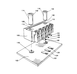
In a specific example, the electrical component to be
surface-mounted on a PCB is an electrical connector block, as
shown in Figure 1. The connector block 100 is made of an
2S insulating material, such as plastic, and is molded to
include at least one point of connection for interfacing with
a mating component or with discrete wires. The connector
block 100 further includes pins 104, 106 and 108, and two
cylindrical apertures 110 and 112. The pins serve as
3
CA 02299837 2000-OS-11
electrical contacts between the connector block 100 and the
PCB 102, while apertures 110 and 112 form a part of the
anchoring system for the connector block 100. The anchoring
system further includes two cylindrical anchors 114 and 116,
having end surfaces 128 and 130. These end surfaces will
hereafter be referred to as retaining surfaces, and will be
described from a functional point of view in further detail
below. Anchors 114 and 116 are hollow and include radially
outwardly projecting shoulders 132 and 134, respectively.
Each shoulder is designed to form an abutment against the
upper surface of the connector block 100 when its respective
anchor is inserted into one of the apertures in the connector
block 100. The length of anchors 114 and 116, between the
lower edge of shoulders 132 and 134, respectively, and the
retaining surfaces 128 and 130, respectively, is
substantially equivalent to the thickness of the connector
block 100. Thus, when the anchors 114 and 116 are inserted
into apertures 112 and 110, respectively, the retaining
surfaces 128 and 130 are coplanar with pins 104, 106 and 108.
The circular cross-section diameter of the cylindrical
anchors 114 and 116 is such that the anchors fit tightly into
apertures 112 and 110, respectively.
The PCB 102 may include multiple integrated circuit
chips and connections for a variety of other electrical
components, none of which are shown in Figure 1 in the
interest of clarity. The PCB 102 further includes a
plurality of solder pads that also form a part of the
anchoring system. Solder pads 122, 124 and 126 are matched
in shape, size and spacing with pins 108, 106 and 104,
respectively, and serve as points of electrical contact as
well as anchoring points once soldered with the pins. Solder
pads 118 and 120 are matched in shape, size and spacing with
the retaining surfaces 128 and 130 of anchors 114 and 116,
4
CA 02299837 2000-OS-11
respectively, and serve as additional anchoring points once
soldered with the anchors.
In use, the connector block 100 is fitted with the
anchors, whereby anchors 114 and 116 are inserted into
apertures 112 and 110, respectively. The dimension matching
between anchors and apertures ensures that once the anchors
are fitted into the apertures, they are tightly retained in
place by friction forces. The anchor-fitted connector block
100 is next placed on the PCB 102, positioned such that the
pins 104, 106 and 108 are aligned with solder pads 126, 124
and 122, respectively, and the retaining surfaces 128 and 130
are aligned with solder pads 118 and 120, respectively. The
placement of the anchor-fitted connector block 100 onto the
PCB 102 may be performed by pick-and-place machinery in an
automated assembly operation, particularly because the
connector block 100 need not be pushed onto the PCB 102. In
effect, the mounting of the anchor-fitted connector block 100
onto the PCB 102 requires zero-insertion force, an important
advantage of this novel anchoring system.
Once properly positioned on the PCB 102, the connector
block pins 104, 106 and 108, as well as the retaining
surfaces 128 and 130, are soldered to the PCB 102. Since
retaining surfaces 128 and 130 are coplanar with pins 104,
106 and 108, an even soldering between the connector block
100 and the PCB 102 is assured. The mounted anchor-fitted
connector block 100 is shown in Figure 2. The tight fit of
the anchors 114 and 116 in the connector block 100 restricts
the movement of the latter on the PCB 102, thus eliminating
undesirable stresses on the electrical pin solder-joints 200,
202 and 204. Note that anchors 114 and 116 form no part of,
and do not interfere with, the electrical contact between the
connector block 100 and the PCB 102. This is ensured by the
positioning of the anchors in the connector block 100 such
that they are spaced apart from connector pins 104, 106 and
5
CA 02299837 2000-OS-11
108, which serve as the points of electrical contact between
the connector block 100 and the PCB 102.
The retaining surfaces 128 and 130 of the anchors are
thin enough to allow for quick heating to soldering
S temperatures. As such a characteristic is common to typical
solder contacts and is well known to those skilled in the
art, it will not be described in further detail. More
importantly, the retaining surfaces 128 and 130 are pierced
to allow molten solder to flow in, thus maximizing the
solder-joint area. Taking for example anchor 114, Figure 3
shows that anchor 114 rests on solder pad 118 of the PCB 102,
surrounded at its retaining surface 128 by solder 300. The
retaining surface 128 is pierced, providing more area for
contact between the solder 300 and the retaining surface 128.
The greater the solder-joint area, the greater the anchoring
force securing the connector block 100 to the PCB 102.
In an alternative embodiment, the retaining surfaces may
be an integral part of the connector block. For example, the
retaining surfaces may be metallic elements embedded in the
plastic molding of the base of the connector block. Further,
the connector block may include a single retaining surface of
greater area, or a plurality of retaining surfaces positioned
strategically about the base of the connector block, so as to
eliminate undesirable movement of the connector block on the
PCB.
The above description of a preferred embodiment under
the present invention should not be read in a limitative
manner as refinements and variations are possible without
departing from the spirit of the invention. The scope of the
invention is defined in the appended claims and their
equivalents.
6