Note: Descriptions are shown in the official language in which they were submitted.
- CA 02300063 2000-02-11
GR 97 P 3581
Description
Residual current device
The invention relates to a residual current
device.
A residual current device is used to ensure
protection against any dangerous fault current in a
electrical system. Such a fault current occurs when a
live conductor part makes electrical contact with
ground. This occurs, for example, when someone touches
a live part of an electrical system or an insulation
fault occurs in the system. The fault current then
flows via the person, as a body current, and in the
system as a fault current, td earth. The residual
current device which is used for protection against
dangerous body currents must then reliably and quickly
isolate the electrical system from the mains power
supply in the event of a fault current which is greater
than the rated fault current, for example 30 mA for
personnel protection and 200 mA for system protection.
The design of a residual current device is
known, for example, from "etz" Volume 107 (1986),
Issue 20, pages 938 to 945. There, Figures 1 to 3, in
particular, show outline circuit diagrams and
functional principles of a residual current device. A
distinction is in this case drawn between two different
fundamental types . A FI circuit breaker, which is also
referred to as a fault-current circuit breaker, is a
fault-current protective device in which the electrical
power required for the switching process is obtained
from the fault current itself, irrespective of the
mains voltage. A so-called differential-current DI
protective circuit breaker is, in contrast, a fault-
current protective device in which the
CA 02300063 2000-02-11
", ,
GR 97 P 3581 -
auxiliary electrical energy required for the switching
process is taken from the mains power supply. Such a DI
circuit breaker thus requires a mains connection and a
power supply unit to operate it, with the power supply
unit converting the mains voltage into the supply
voltage required to operate its components.
While, by virtue of the principle of their
design, FI circuit breakers can trip the circuit
breaker only in the event of an alternating or pulsed
fault current, it is in principle possible, by using
the DI circuit breaker, to detect a direct fault
current and to use this to trip a circuit breaker. By
using a combination of an FI circuit breaker and a DI
circuit breaker, it is thus in principle possible to
monitor an electrical system both for a direct fault
current and for an alternating or pulsed fault current.
The basic circuit diagram of such a so-called all-
current-sensitive residual current device is described,
for example, in "etz", Volume 115, 1994, Issue 16,
pages 896-901. Figure 2 in that document shows a
release for the mechanism of a circuit breaker being
connected both to a fault-current tripping circuit for
alternating and pulsed fault current, and to a fault-
current tripping circuit for direct fault current.
European Patent Specification 0 440 835 also
discloses a combination of a DI circuit breaker and an
FI circuit breaker. The DI circuit breaker which is
intended there to be combined with the FI circuit
breaker comprises a secondary winding (which is
premagnetized with a frequency generator) of a core-
balance current transformer, in which case a device for
balancing the signal curves emitted from the frequency
generator is connected between the frequency generator
and the secondary winding.
CA 02300063 2000-02-11
GR 97 P 3581 P - 3 -
PCT/DE98/02215
However, such a combination is not without its problems
when so-called delayed-tripping FI circuit breakers are
intended to be combined with a DI circuit breaker for
direct fault current. A delayed-tripping FI circuit
breaker is used in order to reduce spurious tripping
due to switching spikes or lightning, or in order to
allow selective disconnection of parts of the system.
Such a delayed-tripping FI circuit breaker, which is
resistant to surge currents, is explained in more
detail, for example, in the "Siemens Journal", Year 42,
Issue 6, 1968, pages 492 to 494. This known FI circuit
breaker is provided, in the secondary circuit, with a
rectifier and a capacitor which is connected in
parallel with the release and produces the tripping
delay. This capacitor connected in parallel with the
release would be charged when a fault-current tripping
circuit (connected in parallel with it) of a DI circuit
breaker responded and applied current to the release,
so that the tripping time would be extended in the
event of a smooth direct fault current. In consequence,
it is not possible to comply overall and in accordance
with the regulations (VDE, OVE, EN, IEC) with the
required tripping delays for alternating, pulsed and
smooth-direct fault currents.
On the other hand, a device for protection
against fault currents is known, which operates with a
first subdevice which is independent of the mains
voltage, and with a second subdevice which is dependent
on the mains voltage (DE-C2-38 23 099). In this case, a
capacitor is arranged in series with a tripping relay
in the first subdevice in order to tune to resonance
for the fault-current evaluation. The second subdevice
is arranged in parallel with the first subdevice as
well as the capacitor, for resonance tuning.
AMENDED SHEET
CA 02300063 2000-02-11
GR 97 P 3581 P - 4 -
- PCT/DE98/02215
The invention is now based on the object 'of
specifying a residual current device in which, in
particular, a delayed-tripping fault-current tripping
circuit for pulsed or alternating current can be
combined with a fault-current tripping circuit for
direct fault current, without the tripping times and
currents influencing one another.
The said object is achieved according to the
invention by the features of patent claim 1. The
residual current device according to the invention
contains a delayed-tripping first fault-current
tripping circuit for alternating and pulsed fault
current, and a second fault-current tripping circuit
for direct fault current, which are connected in
parallel with one another to the control line of a
release for a circuit breaker, with a first means being
provided for electronic decoupling of the first fault-
current tripping circuit from the control line. As a
result of this electronic decoupling, tripping times
and tripping currents cannot influence one another, so
that, when the two fault-current tripping circuits are
combined, the characteristic data for the individual
fault-current tripping circuits, that is to say the
rated fault current and the tripping delay for the
types of fault current respectively associated with
them, remain unchanged even in the combination.
The principle of decoupling for two parallel
measurement channels is known per se (DE-A1-37 18 183).
In a further advantageous refinement of the
invention, the first decoupling circuit comprises a
diode by means of which the first fault-current
tripping circuit is connected to the release. In
consequence, when any current flows in the release
circuit, this prevents charging of the capacitor which
is provided in the first fault-current tripping circuit
in order to delay tripping. In consequence, there is no
AMENDED SHEET
CA 02300063 2000-02-11
' GR 97 P 3581 P - 4a -
PCT/DE98/02215
undesirable tripping delay for the second fault-current
tripping circuit.
In particular, the first decoupling circuit
comprises a discharge resistor which is connected in
parallel with the capacitor, upstream of the diode.
This ensures that the capacitor is discharged
completely.
AMENDED SHEET
CA 02300063 2000-02-11
GR 97 P 3581 - 5 -
A Schottky diode, which has a particularly low
threshold voltage, is preferably provided as the diode.
In a further preferred embodiment, a threshold
value switch is provided in the first decoupling
circuit, which likewise prevents the capacitor in the
first fault-current tripping circuit from being charged
when the second fault-current tripping circuit
responds.
In one particularly advantageous refinement of
the invention, a second fault-current tripping circuit
is provided, whose tripping is likewise delayed, with
second means being provided for electronic decoupling
of the second fault-current tripping circuit from the
control line. This additional electronic decoupling
ensures that tripping times and tripping currents
cannot influence one another even when the tripping of
both fault-current tripping circuits is delayed.
In order to explain the invention in more
detail, reference is made to the drawing, in which:
Figure 1 shows an outline sketch of the circuit
of a residual current device according
to the invention,
Figures 2 and 3 show advantageous refinements of a
first decoupling circuit provided in
the residual current device according
to the invention.
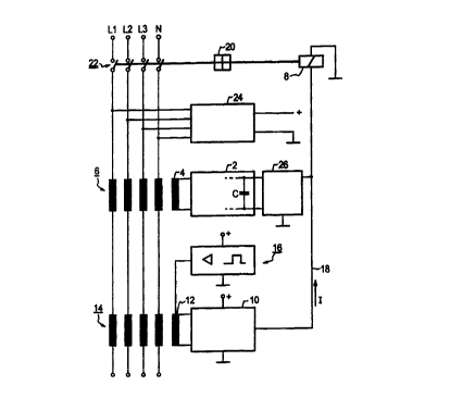
According to Figure 1, an all-current-sensitive
residual current device comprises a first fault-current
tripping circuit 2, which is connected to the secondary
winding 4 of a first core-balance current transformer
6. The first core-balance current transformer 6 is used
to monitor a polyphase network L1, L2, L3, N for
alternating and pulsed fault current.
CA 02300063 2000-02-11
GR 97 P 3581 -
The first fault-current tripping circuit 2
contains a capacitor C which is connected to earth and
is used to delay the tripping of a release 8 (which is
actuated by the first fault-current tripping
circuit 2), for example a coil winding of a tripping
relay.
A second fault-current tripping circuit 10
which is known, for example, from European Patent
Specification 0 440 835 B1 is connected to the
secondary winding 12 of a second core-balance current
transformer 14 and is used for tripping when a direct
fault current is present. The secondary winding 12 of
the second core-balance current transformer 14 has a
pulse generator 16 connected to it, in order to
premagnetize the core-balance current transformer 14,
and which is provided with a device for balancing the
signal emitted from it to the secondary winding 12.
The second fault-current tripping circuit 10
operates the release 8 via a control line 18, by
producing the tripping current I required to trip it.
The release 8 is operatively connected to a switching
mechanism 20, by means of which a circuit breaker 22
can be tripped.
A power supply unit 24 is used to supply
voltage to the second fault-current tripping
circuit 10.
A first decoupling circuit 26 is connected
between the first fault-current tripping circuit 2 and
the control line 18 which leads to the release 8, and
this first decoupling circuit 26 prevents the first
fault-current tripping circuit 2 from producing any
reaction on the tripping response of the second fault-
current tripping circuit 10.
According to Figure 2, the first decoupling
circuit 26 for this purpose contains a diode D, which
is connected in series with the output of the first
fault-current tripping circuit 2, which is used to
prevent
CA 02300063 2000-02-11
GR 97 P 3581 - 7 -
the tripping current I (which flows on the control
line 18 when the second fault-current tripping circuit
trips) leading to charging of the capacitor C1 which is
connected to earth in the first fault-current tripping
circuit 2. Such charging would result in the tripping
of the release 8 being delayed when the second fault-
current tripping circuit 10 responds, when said second
fault-current tripping circuit 10 is operated in
conjunction with the first fault-current tripping
circuit 2, but without the interposition of a first
decoupling circuit 26.
A high-value discharge resistor RE is connected
to earth upstream of the diode D, thus ensuring that
the capacitor C1 is discharged below the threshold
voltage of the diode D, and that the initial conditions
are reproduced. A Schottky diode having a low threshold
voltage, and thus a low power loss, is provided, in
particular, as the diode D.
Diodes having a low threshold voltage, likewise
in particular, Schottky diodes, are preferably also
provided in a rectifier 28 in the first fault-current
tripping circuit 2, in order to reduce the loss that
occurs through the diode D and, despite the connection
of the diode D, to allow the tripping current I (which
is required to trip the release 8) to flow through the
release 8.
In the refinement shown in Figure 3, the first
decoupling circuit 26 contains a threshold-value
switch S1 instead of the diode D (Figure 2), and this
threshold-value switch S1 opens if the first fault
current tripping circuit 2 fails to respond. This
prevents the tripping response of the second fault
current tripping circuit 10 from being influenced by
the connection of the first fault-current tripping
circuit 2.
CA 02300063 2000-02-11
GR 97 P 3581 - 8 -
The tripping of the second fault-current
tripping circuit 10 is preferably likewise delayed and,
to produce this tripping delay, this circuit contains a
capacitor C2 connected to earth and, in this case in
particular, is connected to the control line 18 via a
second decoupling circuit 30, a threshold-value
switch S2 in the exemplary embodiment. This also
prevents the tripping response of the first fault-
current tripping circuit 2 from being influenced by the
presence of the second fault-current tripping
circuit 2.