Note: Descriptions are shown in the official language in which they were submitted.
CA 02300350 2000-03-10
AN ELECTRICAL CONNECTING DEVICE
FIELD OF THE INVENTION
This invention relates in general to electrical connect devices and in
particular, to a connector between electrical drivers on one plane and
actuators on
s a second plane.
BACKGROUND OF THE INVENTION
Connecting means between contact points on two planes are known in the
electronics industry. For example, connection between two printed circuits or
connection between an integrated circuit (IC) under test and the circuit
connecting
~o it for electrical checking.
Recent developments in this field include increasing the quantity and the
density of electrical contacts so as to prevent an increase in the size of the
electrical system containing these elements. US Patents Nos. 5,380,212 and
5,092,774 describe connectors, which are suitable for use where there is a
high
15 density of connectors.
For example, US Patent No. 5,380,212 to Smeenge Jr. et al. describes an
electrical interface which includes an elastomer holder having a plurality of
holes
containing elastomer conductors. US Patent No. 5,092,774 describes an
electrical
connector which provides mechanical coupling and an electrical interface
between
2o circuit boards.
The above prior art references are not suitable where there are a large
number of electrical connections which must be accuracy and precisely located
and where the total size of the contact area is small in comparison to the
board
size (low density).
1 1430-CA
CA 02300350 2000-03-10
US Patent No. 5,599,193 to Crotzer describes an electrical interconnect
method for interconnecting two printed circuit boards, for example, which
provides
a possible solution to this problem. However, the connector is complicated to
manufacture.
1430-CA
CA 02300350 2000-03-10
SUMMARY OF THE PRESENT INVENTION
The present invention provides an improved electrical connector between
contact points on two separate planes, such as circuit boards or other
electronic
components.
s There is thus provided, in accordance with a preferred embodiment of the
present invention, an electrical connecting device for electrically connecting
a
multitude of electrical contacts, which are placed on first and second
electronic
component carrying boards. The device includes an isolating board having a
plurality of apertures formed therein, electrically conductive elements placed
within
~o each of the plurality of apertures and extending therethrough on either
side of the
isolating board. Each of the electrically conductive elements separated and
isolated one from the other. The electrically conductive elements are brought
into
contact with respective electrical contacts on the first and second boards.
Furthermore, in accordance with a preferred embodiment of the present
invention, the isolating board further includes a pair of outer conducting
elements,
located on either end of said electrically conductive elements proximate to
the
outer conducting elements. The pair of outer conducting elements are larger
than
said electrically conductive elements.
Additionally, the isolating board also includes a pair of placement
2o apertures located proximate to the outer edges of the isolating board. The
pair of
placement apertures being dimensionally configured to slidingly receive a
corresponding pair of placement pins attached to the second board.
Furthermore, in accordance with a preferred embodiment of the present
invention, the first board includes a second pair of placement apertures
located
2s proximate to the outer edges of the first board, the second pair of
placement
3 1430-CA
CA 02300350 2000-03-10
apertures being dimensionally configured similar to the first pair of
placement
apertures to slidingly receive the corresponding pair of placement pins
attached to
the second board.
In addition, in accordance with a preferred embodiment of the present
s invention, each of said electrically conductive elements includes an
integrally
molded element having a generally conical shape having upper and lower
truncated cone portions. The upper cone portion has a base having a diameter
d1
and an upper contact area having a diameter d2 and wherein the lower cone has
a
second base having a diameter d3 and a lower contact area having a diameter
d4,
~o the plurality of apertures having a diameter W. W<d4 and W<d3.
Furthermore, in accordance with a preferred embodiment of the present
invention, each of the electrically conductive elements includes a spring
loaded
element having contracts on either side. Alternatively, each of the
electrically
conductive elements includes a dual leaf spring element having contacts on
either
~s side.
Additionally, in accordance with a preferred embodiment of the present
invention, the first and second boards are brought into contact via the
connecting
device by application of a pressure plate applied to the first board. The
overall
dimensions of the pressure plate are at least equivalent to the overall
dimensions
Zo of the first board. The pressure plate includes a flexible and heat
conducting
element suitably attached to the side thereof proximate to the first board.
4 1430-CA
"~.._
CA 02300350 2000-03-10
DESCRIPTION OF THE DRAWINGS
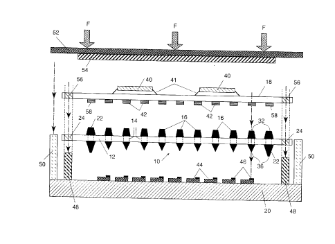
Fig. 1 is an exploded elevational view of a connecting device, constructed
and operative according to a preferred embodiment of the present invention;
Fig. 2 is an enlarged detail of the conductive element of the connecting
device of Fig.1;
Fig. 3 is an isometric illustrative example of first and second boards, which
may be electrically connected together by connecting device of Fig.1; and
_. Figs. 4A-4C illustrate various alternative embodiments of the conductive
element of Fig. 1.
5 1430-CA
CA 02300350 2000-03-10
DETAILED DESCRIPTION OF THE INVENTION
Reference is made to Fig. 1, which is an exploded elevational view of a
connecting device, generally designated 10, constructed and operative
according
to a preferred embodiment of the present invention.
Connecting device 10 comprises an isolating board 12 having a plurality of
apertures 14 formed therein. A plurality of conductive elements 16 are molded
within each of the apertures 14, each of the conductive elements 16 extending
either side of the isolating board 12.
The conductive elements 16, which are isolated one from the other, act as
~o the contact makers between boards, for example, which require to be
electrically
connected together. Connecting device 10, illustrated in the exemplary
embodiment of Fig. 1, is located between a printed circuit board 18 and a
series of
actuators 44 mounted on a metallic ground plate 20.
Isolating board 12, which may be constructed of any suitable insulation
~s material, such as, for example, "Thermount" manufactured by Arlon Inc.,
USA,
further comprises a plurality of conducting elements 22 and placement
apertures
24. Placement apertures 24 are located proximate to the outer edges of the
board
12. Conducting elements 22 are similar to conductive elements 16 being
integrally
molded with the isolating board 12, and are located on either end of the
plurality of
2o conductive elements 16, proximate to conducting elements 22.
Reference is now also made to Fig. 2, which is an enlarged detail of part of
the isolating board 12 illustrating the conductive element 16. Each conductive
element 16 consists of an integrally molded element having a generally conical
shape. Conductive element 16 comprises upper and lower truncated cone
6 1430-CA
CA 02300350 2000-03-10
portions 26 and 28, respectively, which make contact to printed circuit board
18
and the actuators 44 mounted on metallic ground plate 20, respectively.
Fig. 2 illustrates the preferred dimensional structure of conductive
elements 16. Apertures 14 are circular having a diameter W. Upper cone 26 has
s a height h1, a base 30 having a diameter d3 and an upper contact area 32
having
a diameter d2. Lower cone 28 has a height h2, a base 34 having a diameter d4
and a lower contact area 36 having a diameter d1.
In order that the conductive elements 16 are secured in place, the
following relationship should be maintained: W<d4, W<d3.
~o In an exemplary embodiment, isolating board 12 is 0-88 mm thick. The
exemplary dimensions of the corresponding conductive elements 16, are as
follows: W = 1_5 mm, h 1 = 1.4mm, h2 = 1.2 mm, d 1 = 0.25 mm, d2 = 0.8 mm, d3
=
2.0 mm and d4 = 2.0 mm.
Reference is now also made to Fig. 3, which is an isometric illustration of
~s the components of printed circuit board 18 and the actuators 44 mounted on
metallic ground plate 20.
Printed circuit board 18 comprises a plurality of drivers 40 mounted on the
upperside of printed circuit board 18 and a plurality of contact pads 42 on
the
underside of printed circuit board 18, to which drivers 40 are connected.
Zo Generally, each driver 40 comprises leads or pads 41, which are
connected via a conductor (not shown) to contact pads 42.
Printed circuit board 18 further comprises secondary placement apertures
56 (Fig. 1) located proximate to the outer edges of thereof and outer ground
contact elements 58 (Fig. 1 ). Outer ground contact elements 58 are similar to
zs contact pads 42. Elements 56, 58 are shown in Fig. 1 but not in Fig. 3.
7 1430-CA
CA 02300350 2000-03-10
A plurality of actuators 44., arranged in a bi-dimensional array; are
mounted on ground plate 20 each of actuators 44 having its own actuator
contact
pads46. Actuators 44 may be any suitable electrical element such as
piezo-electrical actuators.
s The negative polarity of each of the actuators 44 is in contact with the
metallic ground plate 20, which acts as an earth conductor. The actuators 44
are
activated by an electrical pulse generated from the drivers 40 via the printed
circuit
contact pads 42 and actuator contact pads46.
Metallic ground plate 20 further comprises placement pins 48 and frame
~o supports 50. (Fig. 1) Both placement pins 48 and frame supports 50 are
integrally
connected with the metallic ground plate 20.
Placement pins 48 are dimensionally configured to be slidingly insertable
within placement apertures 24 of isolating board 12 and secondary placement
apertures 56 of printed circuit board 18.
15 Thus, by inserting placement pins 48 into the placement apertures 24, the
lower contact area 36 of conductive element 16 can be precisely placed on
actuator contact pads46. Similarly, by inserting placement pins 48 into the
secondary placement apertures 56, the upper contact area 32 of conductive
element 16 can be precisely located to contact pads 42.
2o The height h2' of the lower cone of the conducting elements 22 is greater
than height h2 of the standard lower cone 28 of conductive elements 16.
Actuators 44 are not placed directly under ground conducting elements 22
so that the longer lower cone of conducting elements 22 makes direct contact
with
the metallic ground plate 20. Thus, the ground circuit to all the actuators is
closed
Zs simultaneously.
8 1430-CA
CA 02300350 2000-03-10
In order to achieve good contact between the various contact points, a
pressure plate 52 (Fig. 1 ) is used. The pressure plate 52 comprises a
flexible and
heat conducting element 54 suitably attached to one side thereof. The overall
dimensions of pressure plate 52 are at least equivalent to the overall
dimensions of
s the metallic ground plate 20.
Element 54 is used for conducting heat created from the drivers 40 to the
pressure plate 52. Element 54 also compensates for variations in the height of
drivers 40. In practice, pressure is applied to the upper surface of pressure
plate
52 (indicated by arrows F) until it makes contact with the frame supports 50
of
~o metallic ground plate 20.
The force required to create a satisfactory contact for a single conductive
element 16 is approximately 10 to 20 grams, for example. Thus, assuming an
average force of 15 grams per conductive element 16, the required force is
approximately 15 Kg. for an array of 1000 conductive elements 16. The
15 parameters which determine the required force for compressing the contact
element 16, include its geometrical characteristics and the elasticity
properties of
the material it is made of.
The conductivity of the contact element 16 is also dependent on the
material it is made of. For example, moldable elastomeric materials including
Zo conducting particles such as "CONSIL-C" manufactured by Tecknit fof
Cranford,
N.J.. U.S.A.1, or similar can conduct up to 0.5 ampere with a resistance of
less
than one tenth of an Ohm.
Pressuring this type of elastomeric material creates contact between the
metal particles within the material and enables electrical conductivity from
the
9 1430-CA
CA 02300350 2000-03-10
upper contact plane 32 to the lower contact plane 36. The quality of the
conductivity is dependent upon the pressuring and the type of the metal
particles.
Reference is now made to Figs. 4A - 4C, which illustrate various
alternative embodiments of conductive elements 16. For example, Fig. 4A
s illustrates a conductive element, generally designated 60, based on a
vertical
coiled spring. Conductive element comprises a central body 62 containing a
coil
spring 64. At either end of the spring 64are attached external contact
elements 66
and 68 for connecting with contact pads 42 and actuator contact points 46,
respectively.
~o Figs. 4B and 4C illustrate a conductive element 70 comprising a pair of
metallic leaf springs78, one on either side of isolating board 12 connected by
a pair
of conducting hole elements 74 as known in the art. As best seen in the
isometric
view of Fig. 4C, each leaf spring 78 comprises a generally triangular base
component 76 on one plane having a tongue element 78 extending from one side
15 Of component 76. Fig. 4C shows only the upper part of conductive element
70.
A contact point 80 is attached to the flexible tongue element 78.A pair 70
of flexible elements 78, comprising a conductive element from tip 80a to tip
80b
can be used as a replacement for conductive element 16 to connect in Fig. 1
contact elements 42 and actuator contact points 46, respectively.
1430-CA