Note: Descriptions are shown in the official language in which they were submitted.
CA 02300425 2000-02-14
WO 99/09536 ~ PCT/US98/14576
TITLE OF THE INVENTION
DRIVE CIRCUIT FOR REACTIVE LOADS
BACKGROUND OF THE INVENTION
The present invention relates generally to a
circuit for driving a reactive load, and more
particularly, to a highly efficient resonant switching
circuit for converting DC current into, sinusoidal
circulating currents in reactive loads at radio
frequencies. The present invention can be used, for
instance, for driving reactive (inductive) loop antennas
such as that used in an interrogator for an electronic
article surveillance (EAS) system.
A drive circuit with a resonant circuit is
commonly used to enable the efficient conversion of energy
from a DC power supply to a reactive load. Fig. 1 shows,
in generalized form, a prior art drive circuit 100 for
driving a reactive (inductive) load 102 (Ls). The drive
circuit 100 includes a current ewitch device Qs, a
resonance capacitor (Cs) and loss element (Ro), the latter
representing the power losses associated with the
resistances of the reactive load Ls 102 and the capacitor
- 1 -
CA 02300425 2000-02-14
WO 99/09536 PCT/US98/14576
Cs and any additional resistance that may be connected to
the circuit 100. The design of the circuit 100 is
optimized for delivering power into the loss element (Ro),
rather than reactive energy into the inductive load (Ls)'.
Thus, the analysis of the efficiency of the circuit 100 is
commonly relative to the amount of power delivered to the
loss element (Ro). The following discussion refers to
this common method of analysis. (An additional resistance
may be made a part of the resonant circuit comprising Ls
and Cs, for example, to increase the resonance bandwidth).
Fig. 2 shows voltage and current waveforms 102,
104 typically associated with the drive circuit 100. The
upper waveform 104 shows the voltage (Vs) across the
current switch device Qs and the capacitor Cs resulting
from the current switching performed by the current switch
device Qs. The lower waveform 106 shows the current (Ils)
that flows through the reactive load Ls.
It is desirable to operate drive circuits for
reactive loads with the highest possible efficiency.
Inefficient drive circuits require larger power supplies.
Inefficient drive circuits also waste substantial power in
the form of heat, and thus require large heat sinks and/or
- 2 -
CA 02300425 2000-02-14
WO 99/09536 PCT/US98/14576
cooling fans for heat removal, and are often less
reliable. The nature of the current switch device Qs
determines the efficiency of the prior art drive circuit
100. In particular, the percentage of the time the switch
device Qs is made to operate in the linear mode, a mode
where the current is made to vary as a continuous function
of time instead of an on/off function of time, determines
the so called class of operation of the prior art drive
circuit 100.
In reactive load driver circuits, such as the
drive circuit 100, the power conversion efficiency is
generally referred to as the amount of power dissipated by
the loss element Ro (the resistive losses of the circuit).
Thus, the power conversion efficiency is the percentage of
the power dissipated in Ro divided by the total power
consumed by the drive circuit 100 (the sum of the power
delivered to Ro and the power dissipated by current switch
device Qs).
Commonly known classes of operation of the drive
circuit 100 are Class A, Class B and Clasa C. Class A
operation refers to operating Qs in the linear mode 100%
of the time. Class A operation is very inefficient
- 3 -
CA 02300425 2000-02-14
PCT/US98/14576
because of the power dissipated across the current switch
device Qs. This power dissipation is caused by the
simultaneous voltage across and current flow through the
current switch device Qs, that results from the linear
mode of operation of Qs. Class A operation of the prior
art drive circuit 100 has a theoretical maximum efficiency
of 25%.
Class B operation of the circuit 100 refers to
operating the current switch device Qs in the linear mode
for about 50% of the time. In other words, the switch
device Qs is made to operate linearly for about one half
of each cycle of the drive waveform. The maximum
theoretical power conversion efficiency for Class B
operation of the prior art circuit 100 is 78.65%, although
practical implementations often achieve less than 50%
efficiency.
Class C operation of the circuit 100 refers to
operating the current switch device Qs in the linear mode
for leas than 50% of the time. In fact, Class C operation
of the circuit 100 may operate the current switch device
Qs predominantly as an on/off switch, thus not making it
suitable for true linear amplification applications. The
- 4 -
CA 02300425 2000-02-14
WO 99/09536 PCT/US98/14576
conduction time diagram shown in Fig. 2 is for Clasa C
operation. Class C operation of the prior art circuit 100
achieves the highest efficiency operation, often between
40% and 80% in practical applications. Such efficiencies
still do not fulfill the objective of the present
invention.
Fig. 3 shows a prior art "flyback" drive circuit
108, commonly used as a horizontal deflection drive
circuit in CRT' displays (televisions and monitors). When
used as a deflection drive circuit in CRT's, the drive
circuit 108 includes a high voltage transformer (Ls), a
current switching device (Qs), and a resonance capacitor
(Ce). The drive circuit 108 may also include a large
value coupling capacitor (Cc), to prevent DC current from
flowing through the deflection coil (Lo) inductance that
would cause horizontal positioning errors in the CRT
display.
The drive circuit 108 may be characterized as a
resonant switching drive circuit because the current
switching device Qs is operated strictly in the on/off
mode. The resonant part of the drive circuit 108 is
formed by the parallel combination of the deflection coil
- 5 -
CA 02300425 2000-02-14
WO 99/09536 PCT/US98/14576
(Lo) and the high voltage transformer (Ls) in conjunction
with the resonance capacitor (Cs). When operated as a
horizontal deflection circuit, the current switching
device Qs is closed for the sweep duration (about 80% of
the total period), causing a flat bottomed voltage
waveform to be applied across the deflection coil (Lo).
(See waveforms Vs and Vo in Fig. 3). During the time that
the current switching device Qs is on, the supply voltage
(Vsp) is applied across the inductors (Ls) and (Lo). As
is well known in the art, the currents that flow through
Ls and Lo increase linearly during this time. This linear
current increase is desirable in that it causes a more or
less linear deflection of the electrons of the CRT as a
function of time, thereby causing a more or less uniform
distribution of information across the screen of the CRT.
When the switching.device Qs opens during the so
called flyback time (about 20% of the total period). the
energy stored in the inductors Ls and Lo is transferred in
resonant fashion to the resonance capacitor (Cs). This
results in the generation of the high voltage half
sinusoid signal across the capacitor (Cs), the peak of
which is much higher in amplitude than the power supply
- 6 -
CA 02300425 2000-02-14
WO 99/09536 PCTNS98/14576
voltage (Vsp). Thus, the voltage across the inductors Ls
and Lo is reversed, as compared to the voltage applied
across them when the current switching device Qs was
closed, thereby causing the current flowing through them
to reverse, which in turn, causes the capacitor (Cs) to
discharge and transfer its stored energy back to the
combination of inductors Ls and Lo. This charge and
discharge of the capacitor (Cs) is known as flyback and
occurs in a sinusoidal manner, thus resulting in the half-
sine flyback pulses that are indicative of the operation
of the drive circuit 108.
The flyback drive circuit 108 converts DC power
to reactive energy at RF frequencies very efficiently.
Since the current switching device (Qs) is used as a
switch, and not as a linear device, the power losses
associated with Qs can be very low. Unfortunately, the
flyback drive circuit 108 is not suitable for driving an
inductive loop antenna because of the high harmonic
content of the signal it generates. These harmonics
radiate, thereby creating a high level of emissions
outside of the frequency range of the intended radiation,
which is unacceptable to government radio regulation
CA 02300425 2000-02-14
WO 99109536 PCT/US98/14576
authorities, such as the U.S. Federal Communications
Commission.
Fig. 4 shows a prior art Class E drive circuit
110 for driving an inductive load (Lo). The circuit 110
includes a current switching device (Qs), a switch
capacitor (Cs), a DC feed inductor (Ls), a resonance
capacitor (Co), the output inductor (Lo) (which may be an
inductive loop antenna), and a loss element (Ro), the
latter representing the power losses associated with the
l0 resistances of Ls, Cs, Co, Lo and any additional
resistance that may be connected to the circuit 110. (As
with the circuit 100 of Fig. 1, an additional resistance
may be made a part of the resonant circuit comprising Lo
and Co, for example, to increase the resonance bandwidth).
Fig. 5 shows the voltage and current waveforms
associated with the Class E drive circuit 110. A half-
sine flyback pulse 112 is produced at the switching device
Qs by the switch capacitor (Cs), the output inductor (Lo)
and the resonance capacitor (Co). A distinguishing
feature of Class E drive circuit 110 is that the AC
component of the current (Ils) 114 in the switch inductor
g
CA 02300425 2000-02-14
WO 99/09536 PCT/US98/14576
(Ls) is much smaller than the DC current 116 flowing
through the switch inductor (Ls).
In the Class E drive circuit 110, the current
switching device Qs is operated as a switch, either on or
off. When on, the current switching device Qs conducts
for the low voltage portion of the half sine wave and
therefore, minimum power is dissipated. When off, no
current flows through the current switching device Qs, and
therefore essentially no power is dissipated. In the
Class E drive circuit 110, the DC feed inductor Ls has a
large value relative to the output inductor Lo, and
therefore does not affect the resonance operation of the
circuit 110. The resonant frequency of the output
inductor Lo and the resonance capacitor Co is chosen to be
nominally at Fo, the switching frequency of the current
switching device Qs. This is so that the resonant circuit
comprising Lo and Co filters out the harmonics of the half
sine signal generated across the switch Qs, thereby
ensuring that the radiated signal output from the inductor
Lo is mostly free of unwanted harmonics. The half sine
portion of the signal Vs shown in Fig. 5 is the result of
the combined action of Cs, Co and Lo.
_ g _
CA 02300425 2000-02-14
WO 99/09536 PCT/US98/14576
In a practical implementation of the Class E
driver circuit 110, the resonant frequency of Cs, Co and
Lo may be slightly higher than the operating frequency Fo.
This is to ensure that signal Vs returns to ground before
the current switch Qs is turned on. This minimizes the
power losses from the current switch Qs associated with
switching. We have determined that a practical
implementation of the Class E driver circuit for use as a
loop antenna driver is unsuitable because a practical
switching device Qs comprises an FET that has a large,
non-linear device capacitance. This device capacitance is
at maximum when the voltage across the device (Vs) is
minimum. In practice, this large non-linear device
capacitance causes the resonance frequency of the circuit
to be dramatically lower during the immediate period after
the FET is turned off. This tends to latch the circuit
such that the drive voltage (Vs) is held low long after
the FET is turned off. This latching effect can last for
more than one cycle, until the current that flows through
the DC feed inductor (Ls) increases sufficiently to charge
the large non-linear capacitance of the FET sufficiently
to pull the circuit out of this state. Thus, in a
- 10 -
CA 02300425 2000-02-14
WO 99/09536 PCT/US98/14576
practical implementation of the Class E driver circuit
110, drive signal cycles may be skipped, due to latching,
either periodically (generating a sub-harmonic signal) or
randomly (generating a chaotic form of noise). Thus, a
practical implementation of the Class E driver circuit 110
is not suitable for use as a driver for a reactive load
such as a loop antenna.
Class A, B and C and flyback drivers are more
immune to such problems because the resonance of these
circuits controls their operation to a much greater extent
than that of the Class E circuit. The inductor Ls in the
Class A, B and C drive circuits 100 of Fig. 1 and the
flyback drive circuit 108 of Fig. 3 is relatively much
smaller in value than the inductor Ls of the Class E drive
circuit 110. With a relatively small value of Ls, the
current increase through Ls (associated with the applied
voltage across it when the current switch Qs is
conducting) charges the non-linear capacitance of
practical switching devices Qs (such as an FET)
sufficiently quickly so that the previously described
latching does not occur.
- 11 -
CA 02300425 2000-02-14
WO 99/09536 PCT/US98/14576
However, circuits using these classes (A, B, C)
of operation are either inefficient or generate
unacceptable harmonics. Despite the availability of many
different types of driver circuits, there is still a need
for a driver circuit that can efficiently drive reactive
loads without the introduction of excessive noise or
harmonics and Which is suitable for driving an inductive
loop antenna. The present invention fulfills such needs.
BRIEF SUN~IARY OF THE INVENTION
1o Briefly stated, the present invention comprises
a circuit for driving a reactive load, such as an
inductive load or a capacitive load, with high efficiency.
The circuit comprises a driver circuit and a coupling
reactance, the coupling reactance being either a capacitor
or inductor. The driver circuit converts DC input current
to RF output current. The reactance is coupled in series
between the RF output of the driver circuit and an output
resonant circuit. One element of the output resonant
circuit is the reactive load. The coupling reactance
performs a series to parallel impedance match from the
driver circuit to the output resonant circuit.
- 12 -
CA 02300425 2000-02-14
WO 99/09536 PCT/US98/14576
Another embodiment of the present invention
comprises a circuit for driving a reactive load with high
efficiency, having a driver circuit, an output resonant
circuit, one element of which is the reactive load, and a
coupling reactance, the coupling reactance being either a
capacitor or inductor. The driver circuit converts DC
input current to RF output current. The output resonant
circuit has an input for receiving the RF output current.
The coupling reactance is connected in series between the
RF current output of the driver circuit and the input of
the resonant circuit for performing a series ~to parallel
impedance match from the driver circuit to the resonant
circuit.
Yet a further embodiment of the invention
comprises a circuit for driving a reactive load with high
efficiency having a driver circuit comprising an
electronic current switch, a flyback inductor and a
flyback capacitor configured to generate an RF output
current, an output resonant circuit, one element of which
is the reactive load, and a coupling reactance, the
coupling reactance being either a capacitor or an
inductor. The driver circuit generates an RF output
- 13 -
CA 02300425 2000-02-14
WO 99/09536 PCT/US98/14576
current by periodically opening and closing the switch at
the RF frequency of operation such that during the period
when the switch is closed, the voltage across the switch
approaches zero, and during the time the switch is open, a
half sine waveform is created due to the resonant action
of the flyback inductor and flyback capacitor. The output
resonant circuit has an input for receiving the RF output
current. The coupling reactance is connected in aeries
between the RF current output of the driver circuit and
l0 the input of the resonant circuit for performing a series
to parallel impedance match from the driver circuit to the
resonant circuit.
Another embodiment of the present invention
comprises an electronic article surveillance system having
an interrogator far monitoring a detection zone by
transmitting an interrogation signal into the detection
t
zone and detecting disturbances caused by the presence of
a resonant tag within the detection zone. The
interrogator comprises a loop antenna for transmitting the
interrogation signal, a resonance capacitor connected
across the antenna and a circuit for driving the resulting
resonant circuit. The driver circuit has an RF current
- 14 -
CA 02300425 2000-02-14
WO 99/09536 PCT/US98/14576
output and a coupling reactance connected in aeries
between the RF current output of the driver circuit and
the antenna resonant circuit. The inductor performs a
series to parallel impedance match from the driver circuit
to the antenna resonant circuit.
BRIEF DESCRIPTION OF THE DRAWINGS
The foregoing summary, as well as the following
detailed description of preferred embodiments of the
invention, will be better understood when read in
conjunction with the appended drawings. For the purpose
of illustrating the invention, there are shown in the
drawings embodiments which are presently preferred. It
should be understood, however, that the invention is not
limited to the precise arrangements and instrumentalities
shown. In the drawings:
Fig. 1 is an electrical schematic diagram of a
prior art drive circuit for driving a reactive load;
Fig. 2 shows voltage and current waveforms
associated with the drive circuit of Fig. 1;
Fig. 3 is an electrical schematic diagram of a
prior art flyback driver circuit;
- 15 -
CA 02300425 2000-02-14
WO 99/09536 PCT/US98/14576
Fig. 4 is an electrical schematic diagram of
prior art Class E power amplifier used for driving a
reactive load;
Fig. 5 shows voltage and current waveforms
associated with the circuit of Fig,. 4;
Fig. 6 is a functional schematic block diagram
of a circuit in accordance with the present invention
which is used to drive a reactive load;
Fig. 7A is an equivalent electrical circuit
diagram of one preferred implementation of the circuit of
Fig. 6 in a single-ended configuration;
Fig. 7B is an equivalent electrical circuit
diagram of a the circuit of Fig. 7A in a push-pull
configuration;
Fig. 8 shows voltage and current waveforms
associated with the circuit of Fig. ?A; and
Fig. 9 is a functional block diagram schematic
of an interrogator suitable for use with the present
invention.
- 16 -
CA 02300425 2000-02-14
WO 99/09536 PCT/US98114576
DETAILED DESCRIPTION OF THE INVENTION
Certain terminology is used herein for
convenience only and is not be taken as a limitation on
the present invention. In the drawings, the same
reference numerals are employed for designating the same
elements throughout the several figures.
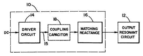
Fig. 6 shows a schematic block diagram of a
circuit 10 in accordance with the present invention which
is used to drive a reactive load. In the embodiment of
the invention shown in Fig. 6, an output resonant circuit
12 is shown comprising at least an inductor and a
capacitor, one of which is the reactive load. The
inductor may be an inductive loop antenna. The reactive
load may comprise either an inductive load or a capacitive
load. Fig. 7A shows a circuit diagram of one preferred
implementation of the circuits 10 and 12.
Referring to Fig. 6, the circuit 10 includes a
driver circuit 14, a coupling or matching reactance (Lm)
16, and an optional coupling capacitor (Cc) 18. The
driver circuit 14 converts a DC supply current (Vsp) to RF
output current. The matching reactance (Lm) 16 is coupled
in series between an RF output 15 of the driver circuit 14
- 17 -
CA 02300425 2000-02-14
WO 99/09536 PCT/US98/14576
and the input of the resonant circuit 12. According to
the present invention, the matching reactance 16 may
comprise either a capacitor or an inductor. The matching
reactance (Lm) 16 performs a series to parallel impedance
match from the output of the driver circuit 14 to the
resonant circuit 12. The optional coupling capacitor 18
is coupled in series between the RF output 15 of the
driver circuit 14 and the matching reactance (Lm) 16 and
blocks the average DC voltage associated with the driver
circuit 14 from appearing at the output resonant circuit
12.
Referring to Fig. 7A, the circuit 10 comprises
the driver circuit 14, shown in equivalent circuit form,
the coupling capacitor (Cc) 18, the matching reactance
(Lm) 16, and the reactive load, either Co or Lo, which is
part of the output resonance circuit 12. The driver
circuit 14 has certain components associated with a Class
E power amplifier, including a switching device (Qs), a
switch inductor (Ls) and a switch capacitor (Cs). The
resonator-equivalent resistance of the driver circuit 14
is represented as Rs. The switching device (Qs) is
preferably a power metal oxide eemiconductor field effect
- Z8 -
CA 02300425 2000-02-14
WO 99/09536 PCT/US98/14576
transistor (MOSFET), but may also comprise any suitable
electronic switching device, such as a power bipolar
junction transistor (BJT), insulated gate bipolar
transistor (IGBT), MOS controlled thyristor (MCT), or
vacuum tube.
Fig. 7A shows the driver circuit 14 implemented
as a single-ended configuration, wherein the active
devices conduct continuously. However, the driver circuit
14 may also be implemented as a push-pull configuration,
as shown in Fig. 7B (i.e., differential implementation),
wherein there are at least two active devices that
alternatively amplify the negative and positive cycles of
the input waveform.
Referring now to Fig. 7B, a push-pull
configuration of a circuit 10' for driving a reactive load
12' is shown. The circuit 10! comprises a driver circuit
14', shown in equivalent circuit form, including a pair of
coupling capacitors (Cc) 18', a pair of matching
reactances (Lm) 16', and the reactive load, which is part
of an output resonance circuit 12'. In accordance with
the push-pull configuration, the driver circuit 14'
includes a pair of switching devices (Qs), a pair of
_ 19 _
CA 02300425 2000-02-14
WO 99/09536 PCT/US98/14576
switch inductors (Ls) and a pair of switch capacitors
(Cs). The equivalent output resistance of the driver
circuit 14~ is represented as resistors Rs. As will be
understood by those of ordinary skill in the art, the
push-pull configuration can have a,higher power-conversion
efficiency and greater output current than the single-
ended configuration. The push-pull configuration also has
other advantages, such as nominally canceled even order
harmonic content. That is, a half-sine flyback switch
waveform output from the driver circuit 14 (discussed in
detail below with respect to Fig. 8) produces only even
order harmonic content and no odd order harmonic content.
In the push-pull configuration, the even order components
substantially cancel each other out, so that substantially
no harmonic content is created. In practice, it is
difficult to produce a perfect half- sine flyback
waveform, so complete cancellation can only be approached.
Referring again to Fig. 7A (and inferentially to
Fig. 7B), the coupling capacitor (Cc) 18 blocks the
average DC voltage associated with the driver circuit 14
from appearing at the output resonant circuit 12. The
- 20 -
CA 02300425 2000-02-14
WO 99109536 PCT/US98/14576
value of the capacitor 18 is sufficiently large so that it
does not affect the operation of the circuit 10.
The matching reactance (Lm) 16 performs a series
to parallel impedance match from the driver circuit 14
(which has a resistance (Rs)) to the load (which~has a
parallel equivalent resistance (Rp), representing the
output resistance of the resonant circuit 12). The driver
circuit 14 resistance (Rs) is lower than the output or
load resistance (Rp). The resonant circuit 12 is not
lossless. Accordingly, a certain amount of power must be
delivered to the resonant circuit 12 for a given
circulating current. At resonance, the power consumption
may be represented by the parallel equivalent resistance
Rp, which is usually too high (e.g., 3K to lOK Ohms) to
allow the resonant circuit 12 to be directly connected to
the output of the driver circuit 14. If such a direct
connection was made, the power transfer would be very
inefficient and insufficient power would be transferred.
It is desirable to transform this high resistance into a
lower resistance (e.g., 5-20 Ohms) to better match the
resistance of the switching device (Qs) and its resonance,
which allows sufficient power to be delivered to the
- 21 -
CA 02300425 2000-02-14
WO 99/09536 PCT/US98/14576
resonant circuit 12 to permit the circuit 12 to drive the
reactive load.
Fig. S showy voltage and current waveforms
associated with the driver circuit 14 of Fig. 7A. The
upper waveform 20 shows the input switching voltage
waveform (Vs), and the lower waveform 22 shows the current
(Ils) through the switch inductor (Ls). The input
switching voltage waveform 20 is a half-sine wave.
When the switching device (Qs) is energized or
l0 closed, the waveform 20 drops to ground (OV) for
approximately one half of the period of operation: The
switch inductor (Ls) charges with increasing current flow
as the supply voltage (Vsp) is dropped across it. As the
current flow through the inductor (Ls) increases, an
increasing amount of energy is stored in the inductor
(Ls). When the switching device (Qs) ie deenergized or
opened for the other half of the period, the waveform (Vs)
rises to a peak voltage in sinusoidal fashion, and the
stored current in the inductor (Ls) discharges while
charging the switch capacitor (Cs) until the stored energy
in the inductor (Ls) is transferred to the capacitor (Cs).
The peak voltage at this point is directly related to the
- 22 -
CA 02300425 2000-02-14
WO 99/09536 PCT/US98/14576
same energy now stored in the capacitor (Cs) as was stored
in the inductor (Ls). The peak voltage causes a reverse
current to start flowing in the inductor (Ls). The
reverse current discharges the capacitor (Cs) in
sinusoidal fashion until the waveform (Vs) returns to
ground. According to the present invention, the inductor
(Ls) and the capacitor (Cs) are sized so that the half-
sine pulse thus formed completes in one quarter to one
half of the operating period. This part of the waveform
is referred to herein as the "flyback pulse," and is
similar in certain respects to the waveform of the CRT
sweep circuit discussed above. The half sine or flyback
pulse has a limited rate of rise which gives the switching
device (Qs) time to turn off while the voltage (Vs} is
rising and which reduces switching transition losses in
the switching device (Qs).
When the switching device (Qs) is on, there is
little or no voltage dropped across it far the current
flowing therethrough. Thus, little power is wasted.
Conversely, when the switching device (Qs) is off, no real
current flows through it (except capacitive) while there
is voltage across it. Thus, even though there is a
- 23 -
*rB
CA 02300425 2000-02-14
WO 99/09536 PCT/US98/14576
voltage drop across the switching device (Qs), little
power is wasted. Theoretically, the circuit 10 is capable
of 100% efficiency. Realistically, losses occur as a
result of the finite on-resistance of the switching device
(Qs). as well as losses associated, with the finite time
required for the switching device(Qs) to transition from
on to off. Typical efficiencies are about 80-90%.
Ideally, the inductor (Ls) and the capacitor
(Cs) of the switch resonator are sized so that, when
damped by the load (output resonant circuit 12), they will
lose all of their stored energy at the completion of the
half-sine pulse. This condition occurs for about 3/4 of a
cycle of the resonant frequency (Fs) of the switch
resonator. In the presently preferred embodiment, the
switch inductor (Ls) and the switch capacitor (Cs) produce
a switch resonance frequency ,(Fs) from between one to two
times the operating frequency (Fo) of the circuit 10.
The peak voltage seen by the switching device
(Qs) for a perfect half-sine flyback waveform is about
2.57 times the supply voltage (Vsp). This is due to the
fact that the average voltage across the inductor (Ls)
must equal zero. Thus, the voltage-time product for the
- 24 -
CA 02300425 2000-02-14
WO 99/09536 PCT/US98/14576
on or low part must.equal the voltage-time product for the
off or high part of the waveform. If the flyback pulse
was a true half sine, then the peak voltage reached would
be n/2 or about 1.57 times the supply voltage (Vsp) over
the supply voltage (Vsp), or about 2.57 times the supply
voltage relative to ground. Since the natural period of
the switch resonator 1/Fs is shorter than one cycle of the
operating frequency (Fo), the peak voltages are generally
higher. The peak voltages are typically three times the
supply voltage (Vsp).
As shown by the lower waveform 22 of Fig. 8, a
distinguishing feature of the driver circuit 14 is that
the AC component of the current in the inductor (Ls) is
larger than the DC current (Idc). The AC component of the
current in the inductor (Ls) causes the current (Ils) to
periodically become negative.. This negative~current
approaches zero in the ideal driver circuit 14. Also, the
current in the inductor (Ls) is not sinusoidal. The
reactance of the inductor (Ls) and the capacitor (Cs) is
much larger than the resistance of the switching device
(Qs) when on. The Q of the switch resonator is less than
one when the switching device (Qs) is conducting, and
- 25 -
CA 02300425 2000-02-14
WO 99/09536 PCT/US98/14576
greater than or equal to two When the switching device Qs
is non-conducting.
An essential difference between the driver
circuit 14 and a prior art Class E amplifier is that the
driver circuit 14 maintains a relatively large resonant
current at the switching device (Qs) by keeping the value
of inductor (Ls) relatively small to eliminate the
latching tendencies of the Class E amplifier, discussed
above: Because the Q of the switch resonator is less than
one when the current switch Qs is on, the waveform
generated by the driver is determined predominantly by the
switch, whereas in Class A, B and C drivers, the waveform
is determined predominantly by the resonator. In this
respect, the driver circuit 14 is similar to the CRT sweep
circuit discussed above, differing in the addition of the
output matching circuit (matching reactance 16). The
switch controlled operation is highly efficient.
As discussed above, the matching reactance (Lm)
16 converts the parallel equivalent resistance of the
output resonant circuit 12 (which is a resonant antenna
comprising an antenna output capacitor (Co) and an output
antenna inductor (Lo)) to an equivalent series resistance
- 26 -
CA 02300425 2000-02-14
WO 99/09536 PCT/US98/14576
that is required to draw the correct amount of power from
the output of the driver circuit 14. When the matching
reactance (Lm) is an inductor, an added benefit is that it
forms a two pole low pass filter with the output capacitor
(Co). This provides reduction of the harmonic energy
generated by the driver circuit 14. Efficient circuits
naturally generate significant harmonic energy due to the
switching nature of the circuits. Thus, for most
applications that desire a single frequency output, this
l0 harmonic energy must be filtered and prevented from
reaching the output.
The value of the output antenna inductor (Lo) is
generally fixed due to known physical constraints on the
antenna, such as allowable size, radiation pattern, and
the like.
The value of the output resonance capacitor (Co)
is selected to resonate the output inductance (Lo) at the
operating frequency (Fo), and is adjustable to allow the
circuit 12 to be precisely tuned to the operating
frequency (Fo), and may be determined by the following
equation:
Co = 1/ (4 n2Fo2Lo) .
_ 27
CA 02300425 2000-02-14
WO 99/09536 PCT/US98114576
The parallel equivalent resistance (Rp) is
primarily determined by the Qo of the output resonance
circuit 12 and to a much lesser extent by the matching
inductor 16, and may be determined by the following
equation:
Rp = QoXLo where XLo ~ 2aLoFo.
To drive a predetermined current through the
reactive load, in this case, Lo, a corresponding voltage
Vo must be developed across the load, and a corresponding
power Po delivered from the driver circuit 14. The amount
of power required depends upon the Q of the output
resonant circuit 12, which is inversely related to the
losses of the resonant circuit 12. For the given current:
Vo = IoXLo; and
Po = Vo2/Rp
where Po .is the power to be delivered by the driver
circuit 14, and XLo is the impedance of the reactance
being driven.
The drive resistance (Rs) is determined by the
amount of power delivered to the output of the driver
circuit 14 based on the supply voltage (Vsp). Since the
signal from the driver circuit 14 is usually filtered
- 28 -
CA 02300425 2000-02-14
WO 99/09536 PCT/US98/14576
prior to the output, only the fundamental frequency
component of the drive signal delivers any significant
power. Also, since the switching device (Qs) waveform is
generally square at its bottom, the peak voltage of the
fundamental frequency component of,the drive signal is
generally equal to the supply voltage (Vsp). The RMS
voltage of the fundamental frequency component of the
drive signal is:
Rs = 0.512 Vsp or Vd = 0.7071 Vsp.
The drive resistance (Rs) can then be calculated by the
following equation:
Rs = 0.5 Vsp2/Po.
The matching reactance (Lm) is sized such that
its reactance at the operating frequency is the geometric
mean between the desired drive resistance (Rs) and the
equivalent parallel resistance (Rp) of the output resonant
circuit 12. In this condition, the parallel resistance
(Rp) produces a certain (Qm) for the inductor (Lm) being
the ratio of reactance to resistance measured at the
operating frequency. The series resistance (Rs) reflected
also produces the same (Qm). The relationship is defined
as follows:
- 29 -
CA 02300425 2000-02-14
WO 99/09536 PCT/US98/14576
QmRs = Rp/Qm = Xlm; or
Xlm = (Rs Rp) lea: and
Lm s Xlm/ (2nFo) .
Thus, this value of the reactance (Lm) is determined,
which is inversely proportional to the square root of the
power delivered to the output.
A minimum preferred value of the switch
capacitor (Cs) is selected by producing a Q of about two
at the anticipated drive resistance for the power
delivered. This Q value causes the resonant energy of the
switching device (Qs) to be completely used in about 3/4
of the switching device (Qs) resonant cycle. At the end
of this period, the flyback portion of the switch waveform
has just returned to zero, ready for the next switch on
time. Since the switch resonance is parallel:
Xcs s R$/2; and
Cs t 1/ (2nFsXcs) ,
wherein Xcs is the impedance of the switch capacitor (Cs).
In practice, the switch capacitor (Cs) is sized to
minimize the effects of the nonlinear output capacitance
of the switching device (Qs). If these nonlinear effects
are not dealt with, they can lead to sub-harmonic and/or
- 30 -
*rB
CA 02300425 2000-02-14
WO 99/09536 PCT/US98/14576
chaotic oscillations as discussed above. A maximum
preferred value for (Cs) is equal to the maximum
capacitance of the current switch (Qs). Under these
conditions, the switch capacitor (Cs) is often larger than
necessary to produce the, damped flyback waveform described
above. This results in higher currents in the switch
resonator. Any undamped energy (reverse Ils) left at the
end of the flyback pulse tries to send the switching
device (Qs) waveform below ground to continue the sine
wave. This is caught by reverse diodes (not shown)
normally associated with the switching device (Qs), or in
the on resistance of the switching device (Qs) itself.
The result is that this stored reverse switch inductor
current is caused to flow back into the supply, thus
returning excess stored energy to the supply. As such,
there is no upper limit to the size of the switch
capacitor (Cs). However, an excessively large capacitor
(Cs) needlessly wastes energy because of the losses
associated with the components comprising the switch
resonator (Qs).
- 31 -
CA 02300425 2000-02-14
WO 99/09536 PCT/US98/14576
The switch inductor (Ls) is sized to produce a
switch resonant frequency from one to two times the
operating frequency, as follows:
Fo < Fs < (2Fo) ; and
Ls = 1/ (4nzFs~Cs) .
Fig. 9 is a schematic block diagram of an
interrogator 24 suitable far use with the present
invention. The interrogator~24 and a resonant tag 26
communicate by inductive coupling, as is well-known in the
art. The interrogator 24 includes a transmitter 10 " ,
receiver 28, antenna assembly 12 " , and data processing
and control circuitry 30, each having inputs and outputs.
The output of the transmitter 10 " is connected to a first
input of the receiver 28, and to the input of the antenna
assembly Z2 " . The output of the antenna assembly 12 " is
connected to a second input of the receiver 28. a first
and a second output of the data processing and control
circuitry 30 are connected to the input of the transmitter
10" and to a third input of the receiver 28,
respectively. Furthermore, the output of the receiver 28
is connected to the input of the data processing and
control circuitry 30. Interrogators having this general
- 32 -
CA 02300425 2004-O1-29
WO 99/09536 PCTlUS98/14576
configuration may be built using circuitry described in
U.S. Patents Nos. 3,752,960, 3,816,708, 4,223,830 and
4,580,041, all issued to Walton.
However, the transmitter 10'' and the antenna assembly
12 " include the properties and characteristics of the
circuit 10 and output resonant circuit 12, described
herein. That is, the transmitter 10 " is a drive circuit
in accordance with the present invention, and the
10 antenna assembly 12 " is part of the output resonant
circuit 12 in accordance with the present invention. The
interrogator 24 may have the physical appearance of a pair
of pedestal structures, although other physical
manifestations of the interrogator 24 are within the scope
of the invention. The interrogator 24 may be used in EAS
systems which interact with either conventional resonant
tags, or radio frequency identification (RFID) tags.
Due to the high efficiency of the drive circuit
10, it is particularly useful when implemented as.a small
printed circuit board using surface mount components,
where heat dissipation is difficult. The drive circuit of
the present invention can control 2000 Volt-Amps of
- 33 -
CA 02300425 2000-02-14
WO 99/09536 PCT/US98/14576
circulating antenna energy at 13.5 MHZ. with about 20W of
power while keeping the harmonics about 50 decibels below
the carrier frequency. This amount of antenna energy is
sufficient to create an interrogation zone for a six foot
aisle using one antenna on each side of the aisle.
It will be appreciated by those skilled in the
art that changes could be made to the embodiments
described above without departing from the broad inventive
concept thereof. It is understood, therefore, that this
invention is not limited to the particular embodiments
disclosed, but it is intended to cover modifications
within the spirit and scope of the present invention as
defined by the appended claims.
- 34 -