Note: Descriptions are shown in the official language in which they were submitted.
CA 02300956 2000-02-18
GR 97 P 8089 Foreign version
- 1 -
Description
Micromechanical electrostatic relay, and a method for
its production
Ttie invention relates to a micromechanical
electrostatic relay having
- a base substrate with a base electrode and with at
feast one stationary contact,
an armature spring tongue which is linked on one side
to a carrier layer connected to the base substrate, has
an armature electrode opposite the base electrode, is
elastically curved away from the base substrate in the
rest state forming a wedge-shaped air gap, and is
fitted at its free end with at least one moving contact
c:~pposite the stationary contact. In addition, the
invention relates to a method for producing such a
relay.
Such a micromechanical relay and an appropriate
a'~-~ production method have already been disclosed, in
principle, in DE 42 05 029 Cl. The essential feature in
this case is that the armature spring tongue, which is
exposed from a substrate, is curved in such a manner
that the armature electrode forms a wedge-shaped air
gap with the opposite base electrode, which air gap,
when a voltage is applied between the two electrodes,
produces a rapid attraction movement on the basis of
the so-called moving-wedge principle. Refinements of
this principle have been disclosed, for example, in DE
49 37 259 Cl and DE 44 37 261 Cl.
In the case of all these known relays with a
micromechanical construction, a relatively high
manufacturing effort is involved since two substrates,
namely on the one hand a base substrate with the base
Plectrode and the stationary contact, and on the other
hand an armature substrate with the armature spring
tongue, the armature electrode and the moving contact,
have to be produced separately
CA 02300956 2000-02-18
GR 97 P 8089 - 2 -
and connected to one another. In addition to the said
main functional elements of the two substrates, further
coating and etching processes are involved, for example
for insulating layers, leads and the like. Each of the
two substrates therefore has to be subjected on its own
to all the complex processes involved before their main
functional layers can be connected, facing one another.
Since the switching elements are also intended to be
protected against environmental influences, an
additional covering part is, as a rule, required as a
closing element, although there is no need to describe
this in any more detail.
In order to simplify production, it would be
desirable if it were possible to form all the
functional elements of the relay on a substrate from
one side. In this case, it is in principle feasible to
form a stationary contact element and a spring tongue
with a moving contact on one and the same substrate, in
which case, for example, the stationary contact and the
~?0 moving contact can be produced one above the other, and
the contact gap can be formed by etching away a so-
called sacrificial layer. Such an arrangement has been
disclosed in principle in US-9 570 139. However, in the
case of the micromechanical switch there, a cavity that
is not accurately defined is created underneath the
armature spring tongue, and this cavity is not suitable
for the formation of an electrostatic drive. In the
case of the switch there, provision is therefore made
for both the armature spring tongue as well as the
stationary contact to be provided with a magnetic layer
in each case, and for the switch to be operated via an
externally applied magnetic field. Even in the case of
t_hP relatively short contact gap which can be achieved
between the moving contact and the rigid stationary
contact using the sacrificial layer technique, such a
rnagnPtic field can be used to produce the required
contact force. However, to do this, an additional
dPVice is required to produce the magnetic field, for
example a coil, and this occupies considerably more
CA 02300956 2000-02-18
GR 97 P 8089 - 2a -
space than is available for a micromechanical relay in
certain
CA 02300956 2000-02-18
GR 97 P 8089 - 3 _
applications.
The aim of the present invention is to develop
the design of a micromechanical relay of the type
mentioned initially such that greater contact forces
can be produced even with the electrostatic drive, but
in which the functional elements of the relay can be
produced on the base substrate by action from one side.
According to the invention, this aim is
achieved in that the at least one stationary contact is
arranged on a stationary-contact spring tongue which,
opposite the armature spring tongue, is linked like
this on one side to a carrier layer and is elastically
curved away from the base substrate in the rest state,
and in that the at least one moving contact is formed
l~> at the free end of the armature spring tongue such that
it projects beyond said armature spring tongue and
overlaps the stationary contact.
Thus, in the case of the invention, in contrast
to previous proposals for micromechanical relays and
(~ .,witches, the stationary contact is also no longer
rigidly arranged on the base substrate but is seated,
like the moving contact, on a curved spring tongue,
which allows an additional switching movement to be
achieved. The moving contact is seated on the armature
'. spring tongue and overlaps the stationary contact. The
prior curvature of the two mutually opposite spring
tongues thus allows an adequate over-travel to produce
the desired contact force to be achieved from the start
of contact-rnaking to the final position of the armature
30 during switching. This effect is achieved even if only
a relatively small free space can be created underneath
the armature when the armature spring tongue is formed
ors a base substrate using the sacrificial layer
technique, by virtue of which relatively small free
35 space the armature is given only a small, specific
over-travel beyond its extended position when
attraction to the opposing electrode occurs.
CA 02300956 2000-02-18
GR 97 P 8089 - q -
Production is particularly advantageous if both
the armature spring tongue and the stationary-contact
spring tongue are formed from the same carrier layer,
and can thus be produced in one and the same etching
process. The spring tongues, whose free ends are
opposite one another, can engage in one another in an
advantageous manner like teeth, so that the projecting
moving contact can be connected, not only at its rear
end but at least on one side as well, to the surface of
the armature spring tongue. The specific design is
dependent on whether the intention is to create a make
contact or a bridge contact.
Silicon is the preferred material for the base
substrate, in which case the carrier layer for the
spring tongues is deposited or bonded on as a silicon
layer with the interposition of the respectively
required functional and insulating layers, and is
etched free in the appropriate processes.
Alternatively, the base substrate may be composed of
glass or ceramic; these materials are considerably more
cost-effective than silicon. However, ceramic requires
an additional surface treatment in order to obtain the
smooth surface required for the relay structures. The
carrier layer which forms the spring tongues may, for
~'S Pxample, be composed of deposited polysilicon or
polysilicon with recrystallisation, or may be an
exposed, doped silicon layer of a bonded-on silicon
wafer. This layer can be produced by epitaxy or
diffusion in a silicon wafer. Alternatively, a
deposited layer of a spring metal, such as nickel, a
nickel-iron alloy or nickel with other additives can be
used in addition to this silicon structure. Other
metals may also be used; the important factor is that
the material has good spring characteristics and
3.5 suffers little fatigue.
An advantageous method for producing a relay
according to the invention has the following steps:
CA 02300956 2000-02-18
GR 97 P 8089 - ~ -
- a metal carrier layer is applied, with the
interposition of an insulating layer and an
intermediate space, to a base substrate which is
provided with a metal layer as the base electrode,
- two spring tongues which are linked on one side
and whose free ends are opposite one another are
formed in the carrier layer,
- at least in places, the spring tongues are
provided with a tensile stress layer on their top
surface,
- a - preferably shorter - spring tongue is provided
at its free end with at least one stationary
contact,
- the - preferably longer - spring tongue is
provided with at least one moving contact which
overlaps the stationary contact, with the
interposition of a sacrificial layer, and
- the curvature of the spring tongues upwards away
from the substrate is achieved by etching the
~0 spring tongues free from one another and from the
substrate.
Further refinements of the production method
are quoted in Claims 19 to 16.
The invention will be explained below in more
detail on the basis of exemplary embodiments and with
reference to the drawing, in which
Figure 1 shows a section illustration of the layout of
the essential functional layers of a micromechanical
relay according to the invention,
Figure 2 shows the micromechanical relay from Figure 1
in the final state (without a casing) in the rest
position,
I~'iyare 3 shows ttoe relay from E'igure 2 irl the operating
position,
Figure 9 shows a plan view of the relay from Figure 3,
which forms a make contact,
Figure 5 shows the same view as Figure 9, but with an
embodiment which forms a bridge contact,
CA 02300956 2000-02-18
GR 97 P 8089 - 5a -
F'iqure 6 shows a modified embodiment ~f
bridge-contact arrangement,
CA 02300956 2000-02-18
GR 97 P 8089 _ 6 _
Figure 7 shows au illustration corresponding to
Figure l, but with a tensile-stress layer above a
partial section of the armature spring tongue,
Figure 8 shows a view corresponding to Figure 2 with
spring-tongue sections of different curvature,
Figure 9 shows a layer structure which is somewhat
modified from that in Figure l, of a base substrate up
to the formation of a carrier layer composed of
polysilicon for the spring tongues,
Figure 10 shows a layer structure, modified from that
in Figure 9, with a carrier layer composed of metal for
the spring tongues,
Figure 11 shows a layer structure, modified from that
in Figures 9 and 10, with a lost-wafer layer bonded on
to the base substrate in order to form the carrier
layer for the spring tongues, and
Figure 12 shows a modified layer structure using an SOI
wafer semi-finished product.
First of all, it should be mentioned that all
the layer illustrations show the layer sequence only
schematically and not the thickness ratios of the
layers.
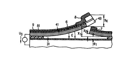
Figures 1 to 3 show the functional layer
structure of a micromechanical relay according to the
;_'S invention based on silicon. In this case, the base
substrate 1 is composed of silicon. This base substrate
is at the same time used as the base electrode;
alternatively, a corresponding electrode layer can be
formed by suitable doping, if required. An insulating
W) layer 2, composed of silicon nitrite for example, is
formed above the base substrate. A first sacrificial
layer 3, which is etched out later, is in turn located
on this insulating layer 2. This first sacrificial
layer 3 is composed, for example, of silicon dioxide
35 and has a thickness dl of, preferably, less than
0.5 Vim. A carrier layer 4 is located above the
sacrificial layer 3, in order to form the spring
tongues. This carrier layer is electrically conductive
and is composed, for example, of polysilicon with a
CA 02300956 2000-02-18
GR 97 P 8089 - 6a -
tta.ick.ness of 5 to 10 Vim. An armature spring tongue 91
and a stationary-contact spring tongue 92 will be
itched out of this carrier layer 4 later.
CA 02300956 2000-02-18
GR 97 P 8089 - 7 _
In the layer structure, they are initially separated
from one another by a second sacrificial layer 5. An
insulating tensile-stress layer 6 is arranged on the
two spring tongues 41 and 42 and, once the spring
tongues have been etched free, produces the upward
curvature of the spring tongues away from the base
substrate, by virtue of its tensile stress. This state
is shown in Figure 2.
A stationary contact 7 is deposited on the
stationary-contact spring tongue 42 by means of an
appropriate coating method, while a moving contact 8 is
formed on the free end of the armature spring tongue 91
in such a way that it overlaps the stationary contact
7, with the interposition of the second sacrificial
layer 5. The height of the switching contacts can be
varied as required, and is typically between 2 and
10 Vim. Depending on the requirement, the thicknesses
and the material compositions of the switching contacts
may also be asymmetric. As is shown in Figure 9, the
two spring tongues 41 and 42 engage in one another like
teeth, so that a central projection 44 on the spring
tongue 92 is surrounded by two lateral projections 93
on the armature spring tongue 41, in the form of
pliers. In this way, the moving contact 8 has three
side sections which rest on the armature spring tongue.
In this configuration, it forms a single make contact
with the stationary contact 7. As can also be seen, the
moving contact 8 has an S-shaped or Z-shaped
cross-ser_tion, in order to ensure the overlap with the
stationary contact 7. The interposed sacrificial layer
typically has a thickness d2 of less than 0.5 ym.
The other required layers are formed in a known
manner, for example a lead 71 to the stationary contact
7, a lead 81 to the moving contact 8, and a further
insulating layer 8 for passivation of the top surface
of the armature spring tongue.
Figure 2 shows the complete arrangement after
the spring tongues have been exposed by etching away
t=he two sacrificial layers 3 and
CA 02300956 2000-02-18
C~R. 97 F' 8089 - g -
5, in which case there is a free space 31 underneath
the armature spring tongue 41. As mentioned, the two
spring tongues 41 and 92 curve upwards because of the
tensile-stress layer 6, so that the arrangement
according to Figure 2 is produced, with an open
contact. The armature spring tongue curves because of
the prestressing to form an unobstructed opening xl at
the spring end. In the same manner, the
stationary-contact spring tongue 42 curves upwards,
after exposure, through the unobstructed opening xz.
~I'hP unobstructed contact gap thus becomes
xK = xi - xz + d2 and approximately
xx = x~ - xz .
'I'tuis unobstructed contact gap x~; can be set as required
by the geometry of the armature spring tongue and the
stationary-contact spring tongue as well as the tensile
stress caused in the spring by the layer 6.
Figure 3 shows the relay i.n the closed
switching state. In this case, the armature spring
!-ondue 91 is resting directly on the opposing
4,.L~ctrode, that is to say it is touching the insulation
layer 2 of the opposing electrode or of the base
substrate. The armature spring tongue is thus bent
downwards by the thickness of the first sacrificial
layer 3, namely dl. This results in an overtravel of
x" = xz - dz + dl, that is to say, approximately
x" = xz.
'this overtravel is independent of the
manufacturing tolerances of the contact heights.
0 As mentioned, Figure 4 shows a plan view of the
.spring tongues 41 and 42 according to Figures 1 to 3.
The shape and the arrangement of the contacts can be
seen in this case, namely of the stationary contact 7
on the projection 99 on the spring tongue 42, as well
as of the moving contact 8, which is attached on three
sides to the projections 93 on the spring tongue 41. In
addition, a hole grid 10 for etching through the first
sacrificial layer 3 is shown by way of indication.
CA 02300956 2000-02-18
c;R 97 P 8089 - g -
Figure 5 shows an embodiment, modified from
that in Figure 9, with a bridge contact. In this case,
the spring tongue 42 has two separate stationary
contacts 7 with corresponding interconnects on two
outer projections 46, while the spring tongue 41 forms
a central projection 47, on which the moving contact 8
rests. A slot H2a in the stationary-contact spring
tongue 42 ensures a high level of torsional flexibility
in order that both contacts close reliably in the event
7.O of an equal erosion. In the case of this example, this
is used as a bridge contact, in that it overlaps the
stationary contacts 7 on both sides.
The same effect can also be achieved with a
structure according to Figure 6. There, an armature
spring tongue 141 is provided with a central projection
147 on which a moving bridge contact 148 rests, which
projects on both sides. This bridge contact 148
interacts with two stationary contacts 144 and 195,
which are seated on two separate stationary-contact
;'U :~F>ring tongues 142 and 143. These stationary-contact
spring tongues 192 and 143 are positioned transversely
with respect to the armature spring tongue 141, that is
to say their clamping-in lines 142a and 143a are at
right angles to the clamping-in line 141a of the
armature spring tongue.
In order to optimize the switching charac-
teristic, it is expedient to curve the armature spring
tongue only in places, as is described in detail in the
documents DE 44 37 260 Cl and DE 44 37 261 Cl. Figures
7 and 8 show schematically a configuration during
production and in the completed state, in which the
armature spring tongue is designed to be only partially
curved. In comparison to Figures 1 and 2, the major
difference is that, in Figures 7 and 8, a
tensile-stress layer 61 extends only over a part of the
armature spring tongue 41, so that a curved zone 62 of
the armature spring tongue is limited to the region of
the clamping-in point, while a zone 63 runs in a
straight line, or with relatively little curvature,
CA 02300956 2000-02-18
GR 97 P 8089 - 9a -
t r:~wards the spring end. In the il.lustratioro in Figures
7 and 8, an insulation layer 69 without any built-in
~~t-rpss is illustrated on the silicon carrier
CA 02300956 2000-02-18
GR 97 P 8089 - 10 -
layer 9, and this insulation layer 64 forms the DC
isolation of the load circuit with the lead Rl from the
spring tongue. The already mentioned tensile-stress
layer 61 is located above this.
S Various methods which are known per se can be
used to produce the layer arrangement described and
illustrated. For example, Figure 9 shows the basic
layer structure on the base substrate 1 as created
using the so-called additive technique. In the case of
lU t:his method, the moving spring tongues and their
carrier layer are produced from a material which is
deposited on the substrate only during production. In
the illustrated example in Figure 9 a wafer composed of
~;-silicon is used as the substrate. A control base
15 electrode 11 is first of all produced on this substrate
n- by diffusion (for example with phosphorus); a
depletion layer 12 is formed between the n-silicon of
the electrode and the p-silicon of the base substrate.
Tine insulation layer 2 and, above this, the sacrificial
rrv layer 3 are applied and structured over the electrode.
The carrier layer 4 is deposited above this, with a
thickness of, for example, 5 to 10 Vim. This carrier
layer 4 is composed of polysilicon or of polysilicon
with recrystallization. The structure of the spring
25 tongues is produced using a conventional mask
technique. The rest of the structure is produced as in
Figure 1. The various functional layers, namely an
insulation layer between the load circuit and the
moving drive electrode, possibly an additional
30 tensile-stress layer and the necessary load circuit
interconnects are thus deposited. In addition, the
described contacts are produced with the interposed
second sacrificial layer as well as any passivation
insulation required for the interconnects.
As already mentioned in the introduction, other
materials may also be used. For example, Figure 10
shows schematically a layer arrangement in which the
~;ubstrate is composed of glass. Alternatively, it could
be composed of a silicon substrate with an
CA 02300956 2000-02-18
GR 97 P 8089 - 11 -
insulation layer, or of ceramic with appropriate
surface treatment. A base electrode 11 in the form of a
metal layer is produced above this substrate. An
insulating layer 2 is then located on this metal layer
and, above this, the sacrificial layer 3. In this
example, an electrochemically applied metal layer is
used as the carrier layer, this metal layer being
composed of nickel or a nickel alloy (for example
nickel-iron), or else of another metal alloy. The
70 important factor is that this metal has a spring
characteristic with little fatigue. Inhomogeneous
nickel layers can be produced by appropriate current
passage during the electrochemical process and these
produce subsequent curvature of the structured spring
tongues. The rest of the construction takes place
analogously to Figure 9 and Figure 1.
A further option for producing the functional
layers of the relay is the so-called lost-wafer
technique. This will be described briefly with
reference to Figure 11 In this case, two original
:substrates are used, although they experience layer
processing from one surface. A base electrode 11 which,
in this example, is recessed in an etched V-groove, is
first of all applied to a base substrate 1 which, in
a'~~ turn, is composed of silicon or of glass. The
insulation layer 2 is located above this base electrode
1. After this, a second silicon wafer 20 with an
n-doped silicon layer 21, which is either applied by
epitaxy or is produced by diffusion, is anodically
bonded to the already structured base substrate 1. This
is followed by the wafer 20 being etched back from the
top surface using electrochemical etching resist so
that only the epitaxial layer 21 remains, and this is
used as the carrier layer for the moving spring
3~ tongues. The step of joining the lost wafer to the base
substrate can also be carried out without the first
sacrificial layer 3 (see Figure 1), provided a free
space 31 can be formed without the insulation layer 2
firmly bonding to the doped silicon layer 21.
CA 02300956 2000-02-18
c;R 97 P 8089 - 12 -
Fi.nal7y, in the case of ttnis example as well,
the structuring of the load circuit elements is carried
out analogously to the additive technique, as has
already been described with reference to Figure 1 and
Figure 6. Thus, for example, an insulation layer 69 for
insulation between the load circuit and the drive
electrode formed by the spring tongue 91, to the extent
that this is required, an additional tensile-stress
layer 61, the load circuit interconnects 71 and 81, the
stationary contact 7, the second sacrificial layer 5
and the moving contact 8 are applied and structured
successively. If any additional layers are required for
passivation insulation, this is done in accordance with
the knowledge within the experience of a person skilled
in the art.
Another option for producing the structure
according to the invention is to use a so-called SOI
wafer (silicon-on-insulator). Figure 12 shows such an
:-~oI wafer as a semi-finished product. The difference
from the construction according to Figure 9 is that the
individual layers are in this case not retrospectively
deposited on the substrate but, instead of this, such
art ~OI wafer as a semi-finished product has a
prefabricated layer structure, in which case an
2~ insulation layer 2, for example composed of silicon
nitrite, a first sacrificial layer 3, for example
composed of silicon dioxide, and a crystalline silicon
~~>itaxial layer as a carrier layer 4 with a thickness
of, for example, 5 to 10 ~tm are arranged on the silicon
substrate 1. The structuring of the load circuit
elements is then carried out on this semi-finished
product analogously to the additive technique described
~~tm~ve, in which case the insulation layer 64, the
additional tensile-stress layer 61, the load circuit
> i_r~ter<-onnects 71 and 81, the stationary contact 7, the
second sacrificial layer 5 (possibly also as
passivation insulation for the interconnects) and the
moving contact 8 are structured as functional layers.
CA 02300956 2000-02-18
GR 97 P 8089 - 12a -
The function of the relay results directly from
the described structure. A control voltage US is
applied to the electrodes
CA 02300956 2000-02-18
GR 97 P 8089 - 13 -
via appropriate connecting elements in order to operate
the relay, that is to say according to Figure 2 to the
substrate l, which is at the same time used as the base
electrode, or to the base electrode (which is
Plectrically insulated from the base substrate)
according to the embodiments in Figures 9 to 11, and to
the armature spring tongue 91, which is at the same
time used as the armature electrode. Electrostatic
charging results in the armature spring tongue 91 being
attracted to the base electrode, as a result of which
the contacts close.
It is also clear to the person skilled in the
art that the structure illustrated in the drawing is
installed in a suitable manner in a casing, so that the
~wr~tacts are protected against environmental
influences. It should also be mentioned that a
plurality of illustrated switching units can be
arranged alongside one another on one and the same
substrate and can be arranged in a common casing, in
order to form a multiple relay.