Note: Descriptions are shown in the official language in which they were submitted.
CA 02301087 2001-10-09
CONTROL CIRCUIT FOR IMAGE ARRAY SENSORS AND
AUTOMATIC HEADLAMP CONTROL
Technical Field
The present invention relates to a control system and more particularly to a
control system
for controlling an image array sensor having a predetermined number of pixels
and controlling
communication between the image array sensor and a microcontroller by way of a
serial
communication interface which allows various subsets of the pixels or
subwindows as well as the
mode of operation of the image array sensor to be efficiently and economically
controlled by way
of a circuit that is adapted to be formed as an application specific
integrated circuit (ASIC) and
even integrated with the image array sensor and the microcontroller to form a
custom IC.
Background Art
Image array sensors are generally known in the art. Both photogate and
photodiode image
array sensors are known. Examples of such image array sensors are disclosed in
U.S. Patent Nos.
5,386,128 and 5,471,515 and 2/SPII=; VOL. 1900,"ACTIVE PIXEL SENSORS: ARE
CCD'S
DINOSAURS?" by Eric R. Fossum, pages 2-14, July 1993. Active pixel image array
sensors are
also known, for example, as manufactured by PHOTOBIT LLC, La Crescenta,
California. Such
active pixel image array sensors are normally provided with a predetermined
number of pixels
forming a window, for example a 50 X 50 window.
There are several important control considerations related to such active
pixel image array
sensors. One important consideration relates to what is
CA 02301087 2000-02-14
WO 99114943 PCT/US98/19075
-2-
commonly known as a windowing function, A windowing function relates to the
ability to control the images of subwindows within the image array sensor for
various purposes. For example, an active pixel image array sensor may be used
for headlamp and tail lamp sensing as part of an automatic headlamp dimming
system. More particularly, in one embodiment of the invention, the image
sensor
is divided up into virtually two identical sized independently positioned
subwindows in one frame through different filters; one for imaging headlamps
and
the other for imaging tail Lamps. In such an application, one row may be
scanned
from the first subwindow and a corresponding row from the other window. The
process is repeated until all of the rows in the subwindows have been scanned.
The windowing function may also be used to control the data
throughput of the system. For example, in the application discussed above, it
is
necessary to discriminate noise, such as road signs and street lamps. In such
an
application, a harmonic analysis may be used to determine if an AC power Line
voltage is present. In such an application, the strongest harnnonic is
normally 120
Hz for 60 Hz line voltage in the U.S. and a 100 Hz for 50 Hz line voltage in
Europe. In order to utilize a Fourier series analysis to detect the 100 and
120 Hz
frequency components, the data must be sampled at a rate which is generally
more
than twice either frequency and divides equally into 1 /50 second and 1 /60
second
full cycle. For example, 6 uniformly spaced samples may be taken at a rate of
300
samples per second for the 50 Hz line frequency and 5 samples at the same 300
sample ger second rate for a 60 Hz line frequency. The 300 sample per second
rate
is about 10 times the usual 30 sample per second frame rate often used for
video
cameras. To avoid excessively high data throughput rates, the frame size may
be
limited to a relatively small size, for example, as small as 2 pixels by 2
pixels.
The windowing feature can also be used for alignment of the
system. For example, a useful field of view for sensing oncoming headlamps of
CA 02301087 2000-02-14
WO 99/14943 PCT/US98/19075
-3-
an approaching vehicle is approximately 10° in elevation by 30°
in width.
However, in such a system it is preferable to allow for some error in the
optical
alignment of the sensor within the vehicle. For example, a sensor with a
I3°
elevational field of view may be provided to allow for a 3 °
misalignment and still
view the proper 10° elevational range. The windowing feature allows the
required
10° field of view to be scanned reducing, for example, better than 20%
of the
image processing data throughput for the function. In particular, in order to
obtain
a proper field of view, a calibration measurement may be taken after the
system
is mounted. The field of view may also be based on the average position of the
image of oncoming headlamps or on an average of the position of a portion of
the
roadway normally illuminated by the controlled vehicles own headlamps which
enables the system to dim the controlled vehicles headlamps based upon an
oncoming vehicle whose headlamps normally appear at an elevation, normally
only a few degrees above the upper extent of the portion of the roadway
illuminated by the controlled vehicles own headlamps.
Another important consideration in an application utilizing an active
pixel image array sensor is the ability to control the sensitivity of the
device. For
certain applications, it may be necessary to adjust the sensitivity of the
system in
order to avoid saturation of the image array sensor. For example, in such an
application, the image of headlamps from an oncoming vehicle appear as bright
spots in the field of view. If the sensitivity of the image array sensor is
set too
high, the particular pixels which image the headlamps will saturate so that
the
actual intensity cannot be determined. In such a situation, since the
intensity of the
headlamp image is a general indicator of the distance of an oncoming vehicle,
such
information is lost. Secondly, the bright image of the headlamps from an
oncoming vehicle is a good indication to the system that the sensed image is
from
an oncoming vehicle rather than being illuminated or reflected from an object
illuminated by the controlled vehicles own headlamps.
CA 02301087 2000-02-14
WO 99114943 PCT/US98/19075
-4-
As such, there is a need to provide improved control of the window
size as well as the modes of operation for such active image array sensors. In
addition to sensitivity and mode of operation adjustments, other parameters,
such
as the frame read repetition timing and the number of frames to be read, also
need
to be controlled. Thirdly, an important consideration is the ability to make
such
changes rather rapidly.
Another important consideration with such systems is the rather
limited space for such control circuits. For example, the automatic headlamp
dimming system is preferably located in the housing which shares a mounting
bracket with the rearview mirror. In such an application, space is rather
limited.
Moreover, as with any control circuit, it is always preferred to reduce the
number
of components in the circuit which normally reduces the cost considerably. For
example, the active pixel image array sensors as discussed above are based on
CMOS technology. Accordingly, there is a need to develop circuitry which can
be
integrated with the image array sensor as well as the microcontroller itself.
Summary Of The Invention
It is an object of the present invention to solve various problems
associated with the prior art.
It is yet a further object of the present invention to provide a control
system for an image array sensor.
It is yet a further object of the present invention to provide a control
system for controlling the communication between an image array sensor and a
microcontroller.
CA 02301087 2000-02-14
WO 99/14943 PCT/US98/19075
-5-
. It is yet a further object of the present invention to provide a control
circuit for controlling various functions of an image array sensor, such as an
active
pixel image array sensor.
Briefly, the present invention relates to a control system for
controlling an image array sensor and controlling communication between the
image array sensor and a microcontroller by way of a serial communication
interface. The control system is able to efficiently control various aspects
of the
image array sensor, such as windowing, mode of operation, sensitivity as well
as
other parameters in order to reduce the data throughput. An important aspect
of
the invention relates to the fact that the control circuit can be rather
easily and
efficiently configured in CMOS with relatively few output pins which enables
the
control circuit to be rather easily and efflcientiy integrated with CMOS based
image array sensors as well as a microcontroller to reduce the part count and
thus,
the overall cost of the system.
Brief Description Of The Drawings
These and other objects of the present invention will be readily
understood with reference to the following Specification and attached
drawings,
wherein:
FIGURE 1 is a top view illustrating the headlamp emission pattern
of a conventional high beam headlamp.
FIGURE 2 is a side cross sectional view of the optical system which
forms a part of the present invention illustrating light rays incident at a
vertical
angle within the desired field of view.
CA 02301087 2000-02-14
WO 99/I4943 PCT/US98/19075
-6-
FIGURE 3 is similar to FIG. 2 illustrating the light rays incident
at a vertical elevation angle beyond the desired field of view.
FIGURE 4 is a top cross sectional view of the optical system
illustrated in FIG. 1 illustrating the light rays at a horizontal angle within
the
desired field of view.
FIGURE 5 is a block diagram of the automatic head light dimming
system in accordance with the present invention.
FIGURE 6 is an overall flow diagram of the image processing in
accordance with the present invention.
FIGURE 7 is a flow diagram illustrating the method for detecting
tail lamps of vehicles within the desired field of view.
FIGURE 8 is a flow diagram for detecting headlamps from other
vehicles within the desired field of view.
FIGURE 9 is a block diagram illustrating an exemplary application
of the control circuit in accordance with the present invention.
FIGURES 10a-lOc are a schematic diagram of the block diagram
illustrated in FIG. 9.
FIGURES l la and l 1b are block diagrams of the registers and the
logic used for a portion of the control circuit in accordance with the present
invention.
CA 02301087 2000-02-14
WO 99/14943 PCT/US98/19075
_'j_
FIGURES 12a and 12b are a top level diagram of the control circuit
in accordance with the present invention.
FIGURE 12c is a schematic diagram of the SerBlk portion of the
control circuit in accordance with the present invention.
FIGURES 12d-12g are schematic diagrams of the CanCtrl portion
of the control circuit in accordance with the present invention.
Best Mode For Carr ing Out The Invention
The present invention relates to a control system for controlling an
image array sensor, such as an active pixel image array sensor, as described
above, for example, a PHOTOBIT photodiode image array sensor and providing
a relatively efficient serial communication interface with a microcontroller.
Although the system is described and illustrated with reference to a
photodiode
image array sensor, the principles of the present invention are also
applicable to
other image array sensors, such as photogate type image array sensors, for
example, as described above. The control system described below is adapted to
be
integrated with existing CMOS image array sensors and even a microcontroller.
The serial communication interface between the microcontroller and the image
array sensor provides for a relatively low pin count device. For example, an
embodiment may integrate the control logic; the programmable row, column and
timing controller; the photo array sensor and associated biasing network; and
the
amplifier and analog to digital converter which represent blocks 1, 2, 3, and
4 of
FIG. 9. Integration of these functions leaves only the microcontroller block 5
as
a major separate block. A ground pin, a V+ supply pin, an oscillator input
pin,
and three pins for a serial interface to the microcontroller may be all of the
pins
CA 02301087 2000-02-14
WO 99114943 PCT/tJS98/19075
_$_
which are required. Even with a V- supply and a serial output pin for a
diagnostic
function, this requires only 8 pins.
The control system in accordance with the present invention is
illustrated in FIGS. 9-12g. An exemplary application of the control system in
accordance with the present invention is illustrated in FIGS. 1-8. However, it
is
to be understood that the principles of the invention are not limited to such
an
application. In particular, the control system in accordance with the present
invention is adapted to be utilized in virtually any application of an image
array
sensor in which one or more of the image array sensor parameters, such as
window size, frame and the various other parameters described above need to be
controlled.
AUTOMATIC HEADLAMP DIMMING SYSTEM
An automatic headlamp dimming system is adapted to provide
automatic headlamp dimming in accordance with the Department of Transportation
(DOT) regulations to provide an intensity of 40,000 cd at 3°, 32,050 cd
at 6°,
1, 500 cd at 9 ° and 750 cd at 12 ° . An example of such an
emission pattern is
illustrated in FIG. 1. The automatic headlamp dimming system which may be
used with the present invention includes an optical system as illustrated in
FIGS.
2-4 and an image processing system as illustrated in FIGS. 5-8. In order to
enable
the high beam headlamps to remain on for the longest reasonable time without
the
subjecting the driver of another vehicle to excessive glare, the automatic
headlamp
dimming system in accordance with the present invention controls the vehicle
high
beam headlamps as a function of the distance as well as the horizontal angular
position of the other vehicle relative to the controlled vehicle. As will be
discussed in more detail below, the optical system is adapted to discriminate
between headlamps and tail lamps of other vehicles. The light rays from the
CA 02301087 2000-02-14
WO 99/14943 PCT/US98119075
-9-
headlamps and tail lamps of other vehicles are spatially segregated on a pixel
sensor array to provide increased discrimination of headlamps and tail lamps
relative to other ambient light sources, such as road signs and reflections
from
snow and the like. The optical system enables both the horizontal and vertical
position of incident lights sources to be determined within the field of view
of the
optical system. The image processing system processes the pixels to provide
for
automatic control of the headlamps as a function of the distance and
horizontal
angular position of another vehicle relative to the control vehicle. As such,
the
system in accordance with the present invention is adapted to provide optimal
control of the vehicle high beam headlamps by allowing the high beam headlamps
to remain on for as long as possible while preventing the driver of the other
vehicle from being subjected to an undue amount of glare.
OPTICAL SYSTEM
Referring to FIGS. 2-4, the optical system includes a pair of lenses
103 and 104, a lens holder 105 and an image array sensor 106. As best shown in
FIGS. 2 and 3, the lenses 103 and 104 are vertically spaced apart in order to
allow
imaging of the same field of view onto different portions of the array. The
lenses
103, 104 image generally the same fields of view because the distance between
the
lenses 103, 104 is relatively small relative to the light sources within the
field of
view of the device.
The lens 103 may be formed with a red filter dye for transmitting
light with wavelengths greater than 600 nm and focusing red light rays 101
from
tail lamps onto one half of the image array sensor 106. The red filter dye
causes
the lens 103 the absorb all light rays at the blue end of the visible spectrum
and
transmit light rays at the red end of the spectrum. As such, the amount of
light
transmitted from non-red light sources, such as headlamps, is greatly reduced
CA 02301087 2000-02-14
WO 99/14943 PCT/US98/19075
-10-
while light rays from tail lamps are fully transmitted through the lens 103.
As
such, the relative brightness of the light rays from tail lamps imaged onto
the
image array sensor 106 is greatly increased.
The lens 104 may be formed with a cyan filtered dye for
transmitting light with wavelengths less than 600 rm. The lens 104 is used to
focus the light rays onto the other half of the image array sensor 106. The
cyan
filter dye has a complementary effect to the red filter described above. In
particular, the cyan filter dye transmits Light from the blue end of the
visible
spectrum while absorbing light from the red end of the spectrum. As such, most
of the light from sources, such as head lights, are transmitted through the
lens 104
while virtually all of the light emanating from tail lamps is blocked.
Both headlamps and tail lamps emit a substantial amount of infrared
light. By utilizing lenses with a filter dye or separate filters which inhibit
light at
wavelengths greater about 750 nm, the infrared light transmitted by the
headlamps
and tail lamps will be substantially blocked by the lenses 103 and 104. By
eliminating infrared light, the ratio between intensity between red lights
imaged
through the red filter and red light imaged through the cyan filter will be
substantially increased.
The use of the red and cyan dyes for the lenses 103 and 104 is
merely exemplary. The filter characteristics of the lenses 103 and 104 are
selected
to optimize the sensitivity of the device to specific light sources. For
example, the
headlamps or tail lamps in new vehicles may be replaced with alternative light
sources with different spectral composition, for example, with high intensity
discharge headlamps and light emitting diode tail lamps requiring different
filter
characteristics. Depending on the spectral characteristics of the headlamps
and tail
CA 02301087 2000-02-14
WO 99/14943 PCT/US98119075
-11-
lamps, transparent lenses I03 and 104 may be utilized with separate color
filters.
The lenses 103 and 104 may be formed as acrylic spherical lenses.
Alternatively, the lenses 103 and 104 may be formed as aspherical lens in
order
to minimize color dispersion and spherical aberration present with spherical
lens.
Complex lenses formed from both spherical and aspherical lenses are also
contemplated.
A single lens may also be used in place of the separate lenses 103
and 104. The use of a single lens may be used to image the field of view onto
a
full or partial color image array sensor containing pigmentation on the
individual
pixels in the array.
As shown best in FIGS. 2 and 3, the horizontal distance between
the two lenses 103 and 104 and the image array sensor 106 is slightly
different.
Offsetting of the two lenses 103 and I04 compensates for the color dispersion
created as a result of the fact that the index of refraction of materials
varies with
the wavelength of light transmitted through it. Because the two lenses 103 and
104 transmit different portions of the visible spectrum, the distance between
the
lenses 103 and 104 and the image array sensor, 106 is optimized to minimize
the
dispersion for the band of light transmitted by each of the lenses 103 and
104.
As mentioned above, the light rays 101 transmitted through the lens
103 are imaged onto one-half of the image array sensor 106 while the light
rays
102 transmitted through the lens 104 are imaged onto the other half of the
image
array sensor 106. In order to provide such spatial segregation of the light
rays
transmitted through the lenses 103 and 104, the lens holder 105 is provided
with
cutouts 107 and preferably formed or coated with a light absorbing material.
CA 02301087 2000-02-14
WO 99/14943 PCTIUS98/19075
-12-
These cutouts 107 prevent light rays beyond the desired maximum vertical angle
transmitted through the red lens 103 from being imaged onto the portion of the
image array sensor 106 reserved for the light rays 102. Conversely, the
cutouts
107 also prevent light rays transmitted through the lens 104 from being imaged
onto the portion of the image array sensor 106 reserved for the light rays
101.
The field of view of the optical system is defined by the
configuration of the lenses 103 and 104 and the cutouts 107 relative to the
image
array sensor 106. For example, an exemplary field of view of 10 degrees in the
vertical direction and 20 degrees in the horizontal directions may be created
by the
configuration set forth below. In particular, for such a field of view, the
lenses
103 and 104 are selected with a diameter of 1.5 mm with a small portion cut
away
to allow the lenses 103 104 to be positioned such that their centers are
separated
by 1.0 mm. The lens I03 is positioned 4.15 mm from the image array sensor 106
while the lens 104 is positioned 4.05 mm away. Both the front and rear surface
radii of the lenses 103 and 104 are 4.3 millimeters with a 0.2 millimeter
thiclaiess.
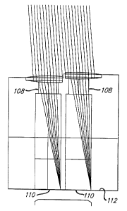
As best shown in FIGS. 3 and 4, circular cutouts 108 are formed
in the lens holder 105. A pair of generally rectangular apertures 110 are
formed
in a rear wall 112. The rear apertures 110 are 1.6 millimeters in the
horizontal
direction and 0.8 millimeters in the vertical direction. As best shown, in
FIG. 4,
the cutouts 107 taper from the rear apertures I10 to the diameter of the front
cutouts 108 to provide the field of view discussed above.
The configuration described above is thus able to baffle light outside
of the desired horizontal and vertical field of view. In particular, FIG. 3
illustrates how the system baffles light rays incident at angles beyond the
vertical
field of view. FIG. 4 illustrates light rays being imaged onto the image array
sensor 106 within the horizontal field of view.
CA 02301087 2001-10-09
-13-
The image array sensor 106 may be CMOS active pixel image sensor array for
example,
as disclosed in U.S. Patent No. 5,471,515 and available from Photobit LLC of
La Crescenta,
California. CMOS active pixel image sensors provide relatively high
sensitivity and low power
consumption as well as the ability to integrate other CMOS electronics on the
same chip. The
image array sensor 106 may be a SO x 50 40,um pixel array. The number of
pixels in the image
array sensor 106 is selected such that not all pixels fall within the area
that the lenses 103 and 104
project onto. The extra pixels allow for simple correction for mechanical
misalignment by
offsetting the expected image location.
The image array sensor 106 provides spatial information regarding light
sources within the
field of view. The number of pixels present in the array is selected to obtain
sufficient spatial detail
although the size of the array is not limited and may be selected and may even
be dictated by
physical and economic limitations. The image array sensor 106 must be
sensitive to accurately
detect tail lights at several hundred feet. Such sensitivity may be achieved
by lengthening the
amount of time the photosites in the array are exposed to light during a frame
period. A frame
period is selected to enable the array to capture and transfer a frame to the
image processing system
in a short enough time to allow the im<~ge processing system to detect another
vehicle entering the
field of view. A short time period also limits the amount of motion within a
frame during the
integration period and thus produces a relatively more accurate instantaneous
image.
The use of a pixel array also provides other benefits. For example, as
mentioned above, the light integration time to capture a frame can be varied.
Such a feature allows
the system to provide optimal results in varying degrees in darkness. Another
important aspect of
an image array sensor is the ability to mtilize subsets of the pixels within
the array or an individual
pixel. As such, as the
CA 02301087 2000-02-14
WO 99/14943 PCT/US98/19075
-14-
window size is decreased, the readout rates can be increased. Such a feature
allows the system to discriminate ambient light sources, such as street lamps.
In
particular, such a feature allows the system to locate a light source within
the
frame and capture several samples of the light sources at a rate several times
greater than 60 hz. In particular, if the samples exhibits 120 Hz intensity
modulation, the light source is likely a street lamp or other light source
powered
from a 60 Hz AC power supply. If the light source is not modulated, the light
source is likely powered by the vehicle's DC power supply.
Another potential benefit of the image array sensor is that it allows
IO the field of view immediately in front of the vehicle to imaged by a higher
pixel
resolution. Thus, the system may be configured such that the effective pixel
resolution decreases as the angle of the vehicle relative to the control
vehicle
increases thus reducing the amount of processing time in those areas. Such a
configuration reduces the sensitivity of the device to light sources from
reflective
stationary objects on the side of the road.
An image array sensor could be manufactured in which the pixel
pitch is varied as a function of the area in the field of view that the pixel
images.
For example, pixels imaging the space corresponding to horizontal angles
within
3 degrees of the center of the vehicle may be provided with a 10 ~,m pixel
pitch.
Pixels imaging horizontal angles between 3 and 6 degrees may be provided with
a 20 ~,m pixel pitch, while those imaging angles greater than 60 degrees may
be
provided with a 40 ~cm pitch. While such a configuration may not increase the
sensing area, the ability the resolve detail increases; an important aspect in
considering that relative size of a tail lamp at a relatively large distance.
For
example, a 41/z inch diameter tail light at a distance of 200 feet subtends an
angle
of less than 0.11 degrees. If a 50 x 50 image array sensor is used to image a
20
CA 02301087 2000-02-14
WO 99114943 PCTIUS98/19075
-15-
degree field of view, the tail lamp would subtend approximately 5.7 % of the
total
area imaged by the pixel.
A tail lamp is relatively brighter than its ambient surroundings,
however, the red light contributed by the tail light is diluted by the ambient
light
at such a distance. Such a factor is critical when comparing the amount of red
light in a given area to the amount of non-red light in the same area. When
the
area of space compared is large relative to the light source, the percentage
of red
light is diminished. By comparison, if 10 ~,m pixels are used in the center of
the
array 106 instead of 40 ~,m pixels, the tail lamp would subtend 90% of the
total
areas, an improvement of 16 times.
IMAGE PROCESSING SYSTEM
The image processing is illustrated in FIGS. 5-8. The image
processing system includes the image array sensor 106, a microprocessor 204,
for
example, a Motorola type HC08, a headlamp control unit 205 and a pair of
headlamps 206. As mentioned above, an active pixel array sensor may be
utilized
for the image array sensor 106. Such an active pixel array sensor includes an
image array 201 and an analog to digital converter (ADC) 202. A timing and
control circuit 203 is used to control the image array 201 as well as the ADC
202
to control the integration time, read out timing, pixel selection, gain offset
and
other variables. The microprocessor 204 is used to analyze the data collected
by
the image array sensor 201. The microprocessor 204 is in communication with
the
headlamp control unit, a conventional unit, implemented, for example, as a
relay,
which, in turn, controls the headlamps 206. The headlamp control unit 205, in
turn, changes the voltage applied to the headlamp 206 to cause the high beam
or
bright lamp to be switched on or off.
CA 02301087 2000-02-14
WO 99/14943 PCT/US98/19075
-16-
. The flow chart for the headlamp control is illustrated in FIG. 6.
The system runs in a continuous cycle with occasional interrupts for absolute
light
measurements, adjustments of ADC parameters or other functions.
At the beginning of each cycle, two images are acquired through the
lenses 103 and 104, as in block 301. In step 302, the images from the lenses
103
and 104 are analyzed to detect tail lamps. Another image is acquired in step
303
through the lens I04. The image acquired through the lens 104 is acquired with
a low enough gain to detect oncoming head lights while rejecting lower light
level
reflections and nuisance light sources. After the images are analyzed, the
system
checks for very bright lights in the image indicating the sudden appearance of
vehicle headlamps or tail lamps within the field of view, as is the case when
a car
turns in front of the controlled vehicle in step 305. If bright lights are
sensed, the
device dims the headlamps 206 immediately and bypasses the time verification
as
discussed below. The cycle is then repeated. If there were no bright lights,
the
system proceeds to step 307 to determine if there are any headlamps or tail
lamps
in the image.
In order to confirm the presence or lack of a headlamp or tail lamp
in a frame, an undim counter and a dim counter are used. These counters
provide
verification of a particular light source whether from a tail lamp or headlamp
from
consecutive frames before signaling the headlamp control unit 205 to dim or
undim
the headlamps 206, except as described above, when a bright light is detected.
By
providing verification, anomalies within the device or in the image will not
cause
spurious operation of the headlamps 206.
The dim counter is incremented each time a frame with a headlamp
or tail lamp is detected until the number of required consecutive frames to
take
action is reached. The dim counter is set to 0 each time a clear frame is
CA 02301087 2000-02-14
WO 99/14943 PCT/US98/19075
-17-
processed. The undim counter is incremented with each clear frame and set to 0
with each frame containing a headlamp or tail lamp. The actual number of
consecutive frames required to dim or undim is determined by the overall speed
of the device. The more frames used for verification, the less susceptible the
system will be to noise and anomalies. However, the device must be able to
react
quickly to be effective so the number of verification frames is kept
relatively low.
Whenever a headlamp or tail lamp is detected in step 307, the undim counter is
set
to 0 in step 308. In step 309, the system checks whether the headlamp 206 high
beams are on. If the high beams are off, no further action is required and the
cycle is repeated as indicated by step 317. If the high beams are on, the dim
counter is incremented in step 310. After the dim counter is incremented in
step
310, the system checks, in step 311, if the dim counter has reached the number
of
consecutive frames required to dim the headlamps 206. If so, the system
proceeds
to step 306 and dims the headlamps 206 and resets both the dim and undim
counters and repeats the cycle. Otherwise, the system repeats the cycle and
proceeds to step to 317.
In step 307, if there are no headlamps or tail lamps in the image,
the dim counter is set to 0 in step 312. Subsequently, in step 313, the system
determines whether the high beams 206 are on. If the high beams are on, the
system repeats the cycle in step 317. In step 314 if the brights are not on,
the
undim counter is incremented. After the undim counter is incremented, the
system
checks in step 315 whether the undim counter has reached the number of
consecutive clear frames required to activate the high beams 206. If so, the
high
beams are turned on in step 316, and the cycle is repeated. If the undim
counter
is less than the required number for activating the bright headlamps 206, the
system repeats the cycle in step 317.
CA 02301087 2000-02-14
WO 99114943 PCT/US98/19075
-18-
The flow diagram for tail light processing is illustrated in FIG. 7.
As will be discussed in more detail below, the primary method of identifying
an
object, such as a tail light, involves comparing the gray scale value of a
pixel
through the lens 103 to a gray scale value of the pixel representing the same
space
imaged through the lens 104. If the value of the pixel imaged through the lens
103
is significantly higher than the value of the pixel imaged through the lens
104, the
light source is determined to be red light. In addition to determining if the
light
is red, the system also checks the brightness of the red light before deciding
that
the light is a tail lamp by determining if the gray scale value of the pixel
is greater
than a threshold value. As is known in the art, the brightness of a light
source
varies with the square of the distance of the light source from the observer.
As
such, an approximate determination of the distance of a leading vehicle can be
made to determine the appropriate time to dim the headlamps.
The threshold value may be computed in a variety of ways. For
example, it can be a predetermined fixed number or a number that is a function
of the current image sensor and ADC settings. The threshold value can also be
determined by computing a threshold as a factor of the average pixel intensity
of
the entire image which would help eliminate variances caused by changing
ambient
light sources. In addition, the pixel value may be compared to the average of
the
pixels in the immediate area of the pixel of interest. This local average
method
prevents relatively large, moderately bright spots in the image from being
seen as
vehicle light sources. More particularly, distant tail lamps subtend less than
one
pixel and thus will only have moderate brightness. Large spots in the image
with
moderate brightness are most likely caused by reflections from large objects.
Close tail lamps which subtend many pixels will have a saturated center which
will
be brighter than the surrounding pixels allowing the same method to detect
them
as well.
CA 02301087 2000-02-14
WO 99/14943 PCT/US98/190'15
-19-
The threshold may also be determined by varying the threshold
spatially by way of a look up table or computation. However, the threshold
should be determined so that dimming occurs appropriately for the dimmest tail
lights allowed by the DOT standards. Distant vehicles are subjected to the
most
intense portion of the controlled vehicle high beam, thus requiring dimming
only
directly in front of the controlled vehicle as indicated in FIG. 1. Thus, a
relatively
low threshold may be selected for light sources imaged directly in front of
the
control vehicle while a higher threshold for light sources that are not
directly in
front of the control vehicle. For example, as discussed in connection with
FIG.
1, the threshold for pixels imaging the field of view 3 degrees right and left
of the
center should correspond to a light level incident on the image array sensor
106
about 4 times as bright as the threshold for red light directly in front of
the vehicle
and 12 times as bright for vehicles at 6 degrees. Such a spatially varying
threshold
helps eliminate false tail lamp detection caused by red reflectors by making
the
system less sensitive to areas of to the sides of the control vehicle.
A similar approach can be taken for varying the threshold for pixels
in imaging areas of space and angles above and below the center. However, a
more conservative approach can be taken when determining the tail light
sensitivity
relative to the vertical angle since vehicles tend to move more frequently and
rapidly in vertical directions due to hills and bumps in the road. Therefore,
specifying relatively tight vertical thresholds may cause the bright headlamps
206
to switch on and off as the vehicle moves several degrees up and down.
A hysteresis multiplier may be applied to the threshold to prevent
oscillations of the headlamps 206 when the light source has a gray scale value
at
or near the threshold. Thus, if the bright headlamps 206 are off, the
threshold will
be lower for al/ pixels to prevent the bright headlamps from coming back on
even
if the faintest tail lamps are present in the image. However, if the bright
CA 02301087 2000-02-14
WO 99/14943 PCT/US98/19075
-20-
headlamps 206 are on, the threshold should be higher so that only tail lamps
of
sufficient brightness are sensed to indicate that the car is within the
dimming range
to cause the headlamps 206 to dim.
One of the biggest problems facing the detection of the tail lamps
is the nuisance red light reflected from corner cube reflectors commonly found
as
markers on the side of the road and on mail boxes. The variable threshold
method
mentioned above helps eliminate some of this noise. However, when a vehicle
approaches a reflector at the proper angles, it is relatively impossible to
distinguish
a red reflector from a tail lamp. Fortunately, by examining successive frames
and
investigating the motion of these objects over time, such reflections can be
filtered. By storing the location of the tail lamps and images over time or by
sensing small region of interest where the tail lamp is located, several
consecutive
times, the device can look for rightward motion and determine if the light
source
is a reflector. Additionally, the speed at which the control vehicle overtakes
a
stationary object is much greater than the relative rate a vehicle would
overtake
another moving vehicle. Thus, the rate of increase in brightness of the object
would be typically much greater for a stationary reflector than for another
vehicle.
This rate of change in brightness coupled with rightward horizontal motion can
be
used as signatures to reduce the number of false tail lamps detected.
A computationally simpler method of analyzing spatial motion of
a light source is to simply take several consecutive regions of the local
region of
interest where the light source is located. Motion in the vertical and
horizontal
directions is relatively slow for tail lamps of a leading vehicle. Sampling a
pixel
a few consecutive times to see if the tail lamp is present in all samples can
adequately eliminate objects which rapidly move within the image.
CA 02301087 2000-02-14
WO 99/14943 PCT/US98/19075
-21-
The flow diagram for tail lamp processing is illustrated in FIG. 7.
Initially, in step 318, the system ascertains if the pixel is within the tail
lamp
window. In particular, as mentioned above, red lights are imaged onto half of
the
image array sensor 106. Thus, if the pixel is not within the appropriate half
of the
image array sensor 106, the system proceeds to step 319 and moves to another
pixel. As mentioned above, there are two criteria for ascertaining whether the
image is a tail lamp. The first criteria relates to comparing the gray scale
value
of the pixel image through the lens 103 with a corresponding gray scale value
for
the same area in space imaged through the lens 104. If the gray scale value of
the
pixel imaged through the lens 103 is significantly larger than the gray scale
value
of the corresponding pixel imaged through the lens 144, one of the criteria
for
detecting a tail lamp is met. Thus, if the pixel of interest is within the
lamp
window as ascertained in step 318, the gray scale value of the pixel imaged
through the lens 103 is compared with the gray scale value of a corresponding
pixel imaged through the lens 104 in step 320. If the gray scale value of the
pixel
image through the lens 103 is not n% greater than the corresponding pixel
imaged
by the lens 104, the system proceeds to step 319 and examines another pixel.
Otherwise, the system proceeds to step 321 and calculates the threshold for
the
particular pixel based on the region of space it images. For example, as
discussed
above, the pixel thresholds may be varied based on their spatial relationship
within
the image array sensor.
As discussed above, the other criteria for tail lamp detection relates
to the brightness of the pixel relative to the neighbor pixels. Thus, in step
322,
the system calculates the average gray scale value of neighboring pixels. If
it is
determined in step 323 that the pixel gray scale value for the pixel imaged
through
the lens 103 is n% greater than the average gray scale value of the
neighboring
pixels, the system proceeds to step 324 and adds the pixel to the tail lamp
list for
future frames of reference. Otherwise, the system moves to step 319 and moves
CA 02301087 2000-02-14
WO 99/14943
PCT/US98I19075
-22-
the next pixel. In steps 325 and 326, the systems determines whether or not
the
red light detected is a tail lamp or a reflector, as discussed above. If it is
determined that the light is a reflector, the system proceeds to step 327 and
moves
on to the next pixel. Otherwise, the headlamps are dimmed in step 328.
The flow diagram for head light processing is illustrated in FIG. 8.
Headlamp detection is similar to tail lamp detection. The primary difference
is
that only the image seen through the lens 104 is utilized. As mentioned above,
the
pixel integration time is shorter and the ADC parameters are such that the
image
only shows very bright objects, such as headlamps. Most reflections have low
intensity light sources that fall well below the zero threshold of the ADC. As
such, pixels are compared to the local average intensity of the neighboring
pixels.
Spatial variances in the thresholds may be set so that pixels corresponding to
the
center of the field of view are more sensitive than pixels on the left of the
image
(left hand drive countries}. These thresholds, however, should not vary
spatially
to the same degree as the threshold for the tail lamps because of the
relatively wide
variance in the emission patterns observed from headlamps. In addition, due to
the relatively higher potential for more glare to the driver of an oncoming
car, the
headlamps may be controlled and dimmed relatively more rapidly than in the
case
when a tail lamp from a vehicle traveling in the same direction is detected.
Similar to the tail lamp processing circuit hysteresis may be added to prevent
cycling of the headlamps.
An additional concern with headlamp detection arises from the rapid
decrease in distance between oncoming vehicles which becomes especially
critical
when an oncoming vehicle suddenly enters the controlled vehicle's field of
view,
for example, when turning a corner or in a similar situation. For this reason,
an
additional flag is used to cause the vehicle to immediately dim the bright
CA 02301087 2000-02-14
WO 99114943
PCT/US98119075
-23-
headlamps and bypass any verification if the light source is above certain
absolute
high level brightness threshold.
The primary nuisance light source complicating headlamp detection
comes from overhead lights, such as street lights and electrically illuminated
street
signs. One method of eliminating such nuisance light sources is to analyze
their
motion. In particular, all overhead street lamps will move vertically upwards
in
the image as the controlled vehicle is moving. Analyzing this motion provides
an
efficient method of detecting some street lamps. Unfortunately, distant street
lamps appear to be at alinost the same elevational angles as distant head
lights and
the rate of vertical climb in the image does not become great until the street
lamp
is closer. However, as discussed above, street lighting is AC controlled and
thus
is subject to 120 Hz intensity modulation. Headlamps powered by DC source do
not exhibit this characteristic. Thus, the image array sensor 106 is able to
utilize
a small number of pixels for taking several rapid consecutive readings in a
window. If the window is small enough, the window can read several hundred
frames per second. Once the light source is identified in the image, several
frames
are read out at a rate of 240 Hz or higher. These readings are then analyzed
to
detect the intensity modulation. If modulation is present, the light source
originates from an AC source and can be ignored. Alternatively, a photodiode
can
used in conjunction with a low pass filter to determine the ratio of light in
the
image that was AC modulated to the unmodulated light. If a significant portion
of the light source is AC modulated, the light source present in the image is
assumed to be from AC light. Otherwise, the light source is assumed to be from
a DC source.
The flow diagram for headlamp processing is illustrated in FIG. 8.
Initially, the system determines in step 329 whether the pixel is in the
headlamp
window (i.e. that portion the image array sensor 106 reserved for light arrays
CA 02301087 2000-02-14
WO 99/14943 PCTIUS98/19075
-24-
imaged through the lens 104). If not, the system proceeds to step 330 and
examines the next pixel. Otherwise, the system examines the pixel in step 331
to
determine if the pixel is modulated at 120 Hz as discussed above. If so, the
light
source is assumed to be a street lamp and thus, the system proceeds to the
next
pixel in step 330. If the pixel is not subject to 120 Hz intensity modulation,
the
system then computes the average gray scale of neighboring pixels in step 332.
In step 333, the system determines the threshold for the particular pixel
based on
the area of the space it images. The system next compares the gray scale value
of
the pixel with an absolute high level threshold in step 334, for example, to
determine if any oncoming cars suddenly come into the field of view of the
controlled vehicle. If so, the system proceeds to step 335 and sets a flag to
cause
immediate dimming. Otherwise, the system proceeds to step 336 and determines
if the gray scale value of the pixel is n% greater than the average of
neighboring
pixels. If not, the system returns to step 330 and examines the next pixel.
1 S Otherwise, the system proceeds to step 337 and adds the pixel to the
headlamp list
for future frames to reference.
The system examines light sources as discussed above in steps 338
and 339 to determine if the light source is a street lamp. If the system
determines
that the light source is not a street lamp, the system proceeds to step 340
and sets
a flag to cause dimming of the headlamps 206. If the system determines that
the
light source is a street lamp, the system proceeds to step 341 and moves on to
the
next pixel. Traditional vehicle lamp systems have the option of the bright
lamps
being either on or off. The present invention is readily adaptable for use
with a
headlamp system where the brights can be activated to a varying brightness
based
on the distance of other vehicles in the field of view. In such an embodiment,
the
brightness of the headlamps may be varied by various techniques including
modulating the duty cycle of the headlamp in order to reduce or increase the
overall brightness level.
CA 02301087 2000-02-14
WO 99114943 PCT/US98/19075
-25-
Variable intensity headlamps also result in better noise filtration.
In particular, whenever a light source is detected which causes the brightness
of
the controlled headlamps of the vehicle to be decreased other images can be
detected to determine if the intensity of these other light sources decreases
by a
similar amount. If so, the system would be able to determine that the light
source
is a reflection from the vehicle's headlamps. Such information can be used as
feedback to provide a relatively efficient means for eliminating nuisance
light
caused by reflections of the control vehicle headlamps. In such an embodiment,
the brightness threshold discussed above would not be used. More particularly,
the brightness of the brightest headlamp and tail lamp in the images is used
to
determine the brightness of the controlled vehicle's headlamps. The brighter
the
headlamps or tail lamp in the images, the dimmer the controlled headlamps.
IMAGE ARRAY SENSOR CONTROL SYSTEM
The control system in accordance with the present invention is
adapted to economically perform the flexible windowing function for the
exemplary application discussed above. There are three important
considerations
in the exemplary application discussed above, for example. First, there is
great
utility in being able to control window size and orientation as well as the
modes
of operation of the image array sensor; for example, in the application
discussed
above, the ability to switch between dual and single window modes of
operation.
Second, other parameters, such as the sensitivity, the frame read repetition
timing,
and the number of frames to read all need to be controlled. Third, in the
exemplary application discussed above, practically every new reading requires
a
major change in setting from the previous reading so it must be possible to
rapidly
change the settings. Even though in such an application, there is a need for
frequent and numerous changes in operational settings, little overhead is
added by
requiring all of the settings to be written before each reading. This also
eliminates
CA 02301087 2000-02-14
WO 99114943 PCT/US98119075
-26-
the need for time consuming address transmissions and for the extra complexity
of a bus structure and address decoding in the image array control circuit.
There are many other considerations for a control system for an
application as discussed above. First, in order to minimize cost and to
provide a
compact control circuit, it is desirable to be able to integrate several if
not all of
the major components of the circuit into a single integrated circuit. In
accordance
with one aspect of the present invention, the control circuit, which, as
discussed
below, includes a serial interface to a microcontroller which can be
integrated on
the same integrated circuit as the image array sensor and can also be
integrated
with various other components, such as an analog to digital converter for
digitizing
the pixel readings. Ultimately, even the microcontroller may be integrated on
the
same integrated circuit chip.
Another consideration for such a control circuit is that the optical
IS window required for the imaging array sensor increases the package cost and
electrical connections are also more expensive to provide in the package with
the
optical window than with conventional integrated circuit packages. For these
reasons, it is highly desirable to use a low pin count serial interface
between the
imaging chip and the microcontroller. It is of further advantage to use the
same
bidirectional serial interface to issue instructions to the image sensor
controller and
to read the digitized image information which is returned. It is of further
advantage to maintain a common serial path, serial registers and timing for
interfacing with the serial port to the microcontroller, continuing to utilize
the
common serial architecture and registers for queuing the instructions, and
finally
for processing the instruction data to perform the required imaging operation.
It
is further advantageous to couple the steps in the successive approximation of
the
pixel reading to the same clock that is used for the above serial instruction
processing and to synchronously transmit the successive bits of the conversion
CA 02301087 2000-02-14
WO 99114943
PCT/US98/19075
-27-
back to the microcontroller, this bit-wise transmission commencing while the
successive approximation steps for conversion of that same pixel are still in
progress. Since a production imaging controller will need custom circuits and
design to apply state of the art technology, the cost of the silicon area will
also be
relatively high at least initially. Thus, it is important for the logic which
couples
the imaging array to the microcontroller and which controls the image sensing
process to be implemented with a modest silicon area. To meet these and other
design objectives, a novel serial architecture is utilized to interface
directly with
a microcontroller to efficiently register the frequently changed instructions
and to
perform the processing to control the rather complicated windowed readout
function.
In an exemplary application, 9 bytes (72 bits) of instruction data are
shifted into 9 byte long shift register segments which are configured as one
serially
contiguous register during the serial load operation. Several eight bit long
registers, each of which must be initialized to a respective value equal to or
determined by one of the values in the main chain, are configured as branches
off
of the 72 bit chain. In one configuration of the invention, the byte wise
serial
order is changed from most significant bit first to least significant bit
first in the
first of the eight bit shift register segments. This is done because the
microcontroller used transmits and receives the most significant bit first and
the
successive approximation analog to digital converter converts and transmits
the
most significant bit first. The serial incrementing circuits must, on the
other hand,
have the least significant bit transmitted first. In two other eight bit shift
register
segments, the value is pre-incremented as it is shifted in. Thus, in the more
general case the simple shift register function is augmented with an
additional
processing step so that the specific register segment is loaded with a
processed
derivative of the serial input value. In an embodiment of the invention, the
timing
for the analog to digital conversion process is common with the timing for the
CA 02301087 2000-02-14
WO 99114943 PCT/US98/190'IS
-28-
serial_processing. A capacitor charge balance analog to digital converter may
be
synchronized to and in fact operated by the same clock which is used for the
serial
processing in the controller and the bits are transmitted over the common
serial
interface to the microcontroller as each successive approximation step of the
S conversion is made. This saves any extra synchronization, control, and
buffering
logic that may be required when the two functions are not synchronized to
operate
together.
The data which is serially loaded as described above preferably
includes the following information. The numbers of the first and the last
columns
of the first frame window are included. Bits indicating the separate options
to
inhibit reset of rows at the beginning of the integration period, to inhibit
readout
of the frames at the end of the integration period, and to select and process
only
the second frame are included. The last of these options is used when the dual
window per frame feature as discussed above for processing headlamps and tail
lamp images is not required. The numbers of the first and last rows of the
first
frame window are included. The row position indicative of the cyclic row
offset
between the row of the frame window which is reset at the beginning of the
integration period and the row of the frame window which is read are also
included in the serial data. The row and column offsets of the second frame
relative to the first are also included for use when the second frame is
selected.
Provision is made to further increase the integration period beyond that
provided
by the cyclic row offset by inserting an integral number of zero or more
additional
integration frame periods (0 to 255, for example) between the reset of a
particular
row in the frame or pair of frames and the reading of the particular row. The
data
also includes the number of times to read the frame or frame pairs to complete
the
instruction.
CA 02301087 2000-02-14
WO 99/I4943 PCT/US98/19075
-29-
The features to selectively inhibit the reset at the beginning of the
integration period or the readout are included so that reset before
integration and
readout after integration can be handled as separate operations. The block
size
required for readout of the whole image at one time may exceed the
microcontroller memory capacity. The readout operation resets only the rows
which are read. For low light levels, it is necessary to use relatively long
integration periods. The limited microcontroller memory may require the image
to be broken into blocks so that the processing of each does not require more
memory than is available. Without separate reset and read instructions, this
would
require very elaborate control or make it necessary to wait for the entire
integration period to process each block. Efficient use of the sensor in low
light
conditions calls for collecting light over as much of the sensor area as
possible as
much of the time as is possible. Since for long integration periods, the
timing is
not ordinarily as critical, the integration can be placed under the control of
the
microcontroller if the available control modes permit. This capability is
provided
for this reason. Furthermore, since windows of non-overlapping rows do not
reset
rows outside of their range during either reset at the beginning of the
integration
period or reset as part of the readout function, the field may be broken into
windows with non-overlapping rows which are reset on a staggered schedule
using
separate instructions which inhibit the readout function but enable the reset
function. The microcontroller may then initiate successive readout and
processing
of these blocks each after an acceptable integration period by inhibiting the
reset
function and enabling the readout function. Either the dual or single frame
modes
may be selected. In this way, the integration period for processing of
multiple
blocks may be overlapped with a minimal increase in the complexity of the
controller circuit. In the above sequence, the integration period for each
instruction
is normally set to a minimum value since the actual integration period is
determined by the microcontroller and a single readout cycle of the single or
dual
frames is normally selected.
CA 02301087 2000-02-14
WO 99/14943 PCT/US98119075
-30-
The embodiment illustrated is configured to interface with and
control an array of photodiode pixel sensors, for example as discussed above.
In
general, the charge at each of the photo sites in a row is drained off when
the row
is reset. Charge is then accumulated when electrons are freed as photons
strike the
photo site so that, for a relatively wide range of light levels and
integrating times,
the accumulated charge is approximately proportional to the product of the
integrating time and the light level. Thus, the integration period as
described above
is analogous to the exposure time with a camera and film.
In one embodiment, a successive approximation analog to digital
converter is utilized and, to minimize the buffer memory and control logic,
the
bits are shifted back to the microcontroller as the successive approximations
are
made with minimal buffering provided to optimize clock timing on the serial
bus
to the microcontrolier.
Following the receipt of the read instruction data, the control system
responds preferably on the same serial interface with the serially transmitted
digitized readings which indicate the light level received by each of the
pixels in
each of the frames specified by the instruction. This reading sequence is
repeated
the number of times specified in the instruction. The microcontroller, for
example, a Motorola 68HC708XL36, utilizes a direct memory access function
which may be utilized to increase rates at which data can be transferred to
the
microcontroller from the photo sensor and to free the microcontroller for
other
functions. One drawback is that the direct memory access function of the
particular
microcontroller is limited to blocks of 2S6 bytes at a time. Each pixel
reading is
encoded as an 8 bit value so the 256 bytes can store readings from only 256
pixels.
With a nominal 64 by 64 pixel array for the dual frame sensor for the rain or
headlamp dimmer sensors, if for example 60 bits corresponds to 30 degrees,
then
a 10 degree by 30 degree field will contain 1200 pixels, and the corresponding
two
CA 02301087 2000-02-14
WO 99114943 PCT/US98/19075
-31-
color dual frame will contain 2400 pixels. This field may have to be read and
processed in blocks to prevent overrunning the available memory in the
microcontroller and before the memory limit is reached. To use the direct
memory
access feature of the selected microcontroller, the data will need to be
collected in
blocks of 256 bytes or less. In one embodiment, there is an' interval equal to
the
time required to transmit 5 successive pixels in a row at the beginning of
each new
row. To utilize the direct memory access feature when more than one block of
data
must be collected for a particular read instruction, the block length is
preferably
set so that blocks end on row boundaries and an interrupt mode is selected so
that
the microcontroller is interrupted at the end of each block which is received.
The
microcontroller then has the five pixel interval to set the direct memory
controller
to receive the next block of data. This between row delay time is used by the
control circuit to issue the reset to the row to start its integration period
and to
transfer the charge from pixels in the row to capacitors for readout. This
process
is detailed in the circuit description which follows. The five pixel delay
period
between rows may optionally be made variable or changed to some other fixed
delay period. However, the between row delay period for a given read operation
is preferably made a consistent length even though not every function
performed
during this period is performed every time. The benefit of the consistent time
period is that the control logic is less complicated as is the computation of
the
frame reading interval. Also, a variable period, depending on the pattern of
the
variation, could make repeated frame readings non-periodic which would create
problems in the harmonic analysis. The microcontroller used may optionally be
replaced by a digital signal processor or other programmable data processing
device.
Referring to FIG. 9, a block diagram of an exemplary control
system which incorporates an image array sensor and microcontroller for use
with
the present invention is illustrated. The system includes a programmable
CA 02301087 2000-02-14
WO 99/14943 PCT/US98/19075
-32-
row-column and timing controller l, control logic 2, an image array sensor 3,
an
amplifier and analog to digital convertor (AID) circuit 4 and a
microcontroller 5.
The present invention relates to the control logic 2 and programmable row-
column
and timing control circuit 1 for controlling the image array sensor 3 and
providing
a bidirectional serial communication interface 6 with the microcontroller 5.
As will
be appreciated by those of ordinary skill in the art the programmable row-
column
and timing control circuit 1 as well as the control logic circuit 2 which form
the
present invention may be implemented as an ASIC and integrated with one or
more of the following portions of the overall circuit: microcontroller 5;
image
array sensor 3 and amplifier and AID convertor circuit 4.
FIGS. l0a-lOc are a schematic diagram of the block diagram
illustrated in FIG. 9. As shown in FIGS. l0a-lOc, the control circuit in
accordance
with the present invention, which, as mentioned above incorporates the control
logic 2 and programmable row-column and timing controller 1, is shown
implemented, for example, as an ASIC XC4003E.
FIGS.12a-12b is the top level schematic diagram used to generate
the program for the ASIC XC4003E as shown in FIG, 10b. FIGS. 12a-12b along
with the referenced lower level diagrams are implemented using Workview
OfflceTM, Version 7.31, Feb. 6, 1997, Viewlogic Systems, Inc. in combination
with the Unified Library from Xilinx, Inc. These schematics are used to
generate
a net list which may be processed by the Xilinx Design Manager version M1.3.7.
The bit stream generated by the component programs of the Xilinx Design
manager may be used to program the ASIC XC4003E. The Atmel AT 17C65 serial
memory in FIG. lOb is configured to store and automatically download the
program to the XC4003E each time that power is first applied to the circuit.
CA 02301087 2000-02-14
WO 99/14943 PCT/US98/19075
-33-
FIGS. 1 la and l 1b depict the registers and the data paths where the
image array sensor instruction data is stored and manipulated for the control
of the
image array sensor. The overall function of the registers is to generate the
sequence of row select and column select addresses required for the dual
windowed readout of the sensor and to return status signals which expedite the
control of the readout sequence. Blocks 300 and 320 in combination generate
the
column select address CSOO through CS06. Blocks 330 and 340 in combination
generate the row select address RS00 through RS06. Block 360 counts the
number of frames which are added to lengthen the sensor integrating time.
Finally
block 370 counts the number of times to read the frame or frame pair to
complete
the instruction sequence.
There are two general modes of operation for the control circuit;
the first is the instruction serial load mode in which the register is
seriaily loaded
with 72 hits (nine serially transmitted bytes) of data. The second mode of
IS operation is the instruction execution mode in which the registers are
reconfigured
and selectively enabled for 8 clock cycle sequences to perform the
incrementing,
loading, and compare functions required to generate the complicated sequence
of
addresses and the status indicating outputs required to sequence the
controlled
windowed readout of the array sensor. The circuit generates binary row and
column addresses which are decoded by the array sensor to select the
appropriate
rows and pixels at the intersection of the selected row and column in order to
perform the required control and readout functions.
The control signals input to the blocks 300, 320, 330, 340, 360,
and 370 are enumerated in the respective lists, 301, 321, 331, 341, 361, and
371
and the signals which are output from these blocks (excluding the
interconnections
which are shown) are enumerated in the respective lists 302, 328, 332, 342,
362,
and 372. Each of the blocks receives a clock signal CLK, a serial load signal
SLD,
CA 02301087 2000-02-14
WO 99114943 PCT/US98/19075
-34-
and a, signal LAST indicating that this is the last of a group of 8 clock
signals for
which a particular block or group of blocks is enabled is used by every block
except block 330. Each of the 72 rectangular boxes in the groups SCOxF, LCxF,
HCxF, SROxF, LRxF, ARxF, HRxF, IFDxF, and RFCxF depict individual
clocked D type flip-flops which have a clock enable. These flip-flops are all
enabled and configured generally as one long shift register to load the 72 bit
(9
serially transmitted bytes) instruction word. Except for the 8 bit group
SCOxF, the
remaining eight flip-flop groups are simple 8 bit shift registers each with a
clock
enable. During the load sequence, SCOxF receives bit 7 through bit 1 of each
byte
shifting them serially into SC07F through SCO1F so that just prior to the last
of
the eight clock pulses which shift in the byte, bit 7 is in SCO1F and bit I is
in
SC07F. Then on the last of the 8 clock pulses, LAST is asserted directing bit
0
coming in last on SRCV directly into SCOOF and exchanging SCOIF with
SC07F, SC02F with SC06F, SC03F with SC05F and leaving SC04F
unchanged. This reverses the order of the bits of the byte so that successive
bytes
are serially transmitted least significant bit first from SCOOF to LCIN and
the D
input of LC7F. This is necessary for the serial add functions performed in
blocks
320, 340, 360, and 370. The SCOxF group was placed first because its value
remains static like SROxF during the execution phase and is not enabled during
that phase. This eliminates the need to further complicate the data selectors
which
are used to reverse the transmission order from most significant bit first to
least
significant bit first. The four low order bits SCOO to SC04 are sign extended
by
repeating SC04 for the higher order bits of adder 307. This number transmitted
on
bus 303 is the column offset of the second frame relative to the first in
signed,
twos complement form which is added in adder 307 to the column address for the
first frame which is generated in ACO through AC7 and transmitted on bus 304.
The adder output is transmitted on bus 305. The signal SSF is asserted to
select
the bus 305 to which the second frame offset has been added and gate it to bus
306. When SSF is not asserted, the signal 304 is gated directly to 306 without
CA 02301087 2000-02-14
WO 99/14943 PCT/US98/19075
-35-
adding the column offset value. CSOxF is a D type register into which the row
address from 306 is clocked by the rising edge of CCLK. The number of bits in
the CSOxF register may be changed to accommodate the number of columns of
pixels in the sensor. 32 to 64 columns and rows are anticipated to be the
number
required for the headlamp dimmer control and the moisture sensing applications
discussed above. The number of bits in the row and column select addresses may
be reduced for smaller numbers of rows and columns or increased to eight to
accommodate up to 256 rows and or columns with few if any other changes. More
rows or columns are within the scope of the invention but will require other
adjustments in the word sizes. It is not necessary to stay with a word size of
eight
but this is convenient to match the byte size of the words in the
microcontroller
memory and in the 8 bit word size of the serially transmitted data.
During the serial load stage, data selector 322 routes the output
signal SCOO to LCIN which is the D input to the LC7F flip-flop. Data selector
324 routes the identical bit stream to the D input of AC7F and data selector
325
routes the output of LCOF to the D input of HC7F. At the completion of the
instruction load phase, the eight bit registers LCxF and ACxF both contain the
address of the starting or low column of the first frame and HCxF contains the
address of the last or high column of the first frame. The count in ACxF thus
begins at the lowest column address and is incremented until it matches the
high
column address. On the next pixel count after the high column address is
matched,
a copy of the low column address is again shifted into ACxF so that the
incremental count from the low to the high column address is repeated. Thus
the
increment pixel count is a simple serial add one operation until the count
equals
the high column address and it is then a copy operation of the low column
address
into the ACxF count register for the next increment operation.
CA 02301087 2000-02-14
WO 99/14943 PCT/US981I9075
-36-
The logic depicted in block 320 is self contained in that it performs
the incrementing, the comparing and the copying as required to produce the
sequence described above. It does so in response to a series of eight cycles
of the
CLK input for which the enable pixel count EPXC input is high. On the first of
the eight CLK cycles, FIRST is asserted and is used by the serial add one
circuit
326 to force the addition of one to the least significant (first) bit of the
ACxF
count. The serial add one circuit 326 contains several gates and only one flip-
flop
to register the carry. The serially incremented output ACA is selected by
selector
324 except during the serial load or reset count cycles so that the
incremented
value appears in ACxF after 8 enabled clock cycles. During each of the
increment
operations EPXC also enables LCxF and with SLD low, LCO is routed to LOIN
which is the D input to LC7F. Thus, at the end of eight enabled clock cycles,
the
original contents of LCxF is re-circulated to its starting position so the
value of
LCxF retains its original low column address. The high column address HCxF is
re-circulated in the same way and the new serialized value of ACxF at ACIN is
compared in a bit-wise fashion with the serialized high column address at
HCIN.
The serial compare function is performed by block 327 which contains only two
flip-flops and several logic gates. One of the flip-flops keeps track of the
bit-wise
equality of the count and the high column address while they are serially
presented
to the comparator and the other is used to assert the ACEH output signal
during
the next eight clock cycles for which EPXC is asserted after the count in ACxF
is
equal to the high column address from HCxF. FIRST is used to initialize the
serial
compare equal indication and LAST is used to signal the required update of
ACEH. Note that, in this way, ACEH is asserted for exactly the number of clock
cycles needed to copy the low column address into the counter. Also, ACEH is
output and fed as an input to the control circuit to signal the end of a row.
There
is a five pixel pause in the otherwise periodic enabling of the EPXC between
rows
so that the required row specific functions may be performed. Otherwise,
during
the entire execution period for the instruction, the column count is regularly
CA 02301087 2000-02-14
WO 99114943 PCT/US98/19075
-37-
incremented whether a pixel value is being read or not so that the pixel count
periodically cycles to create the periodic assertion of ACEH which is used to
enable the row count which is cycled in a similar fashion to cycle the
integration
frame count which in turn increments the frame read count until the required
number of frames have been read. The CCLK signal is asserted only when the
count ACxF is in its rest position between the first and last clock periods of
the 8
clock sequence so that the bits registered in the column select register are
not
shifted to an incorrect position.
Blocks 300 and 320 together generate the column address and are
also cycled as just described to establish the periodic row time base. Blocks
330
and 340 perform a similar but not identical function to generate the row
addresses
and to create periodic frame scan timing signals. The description will be
directed
to the differences. In the intended application, the second frame column
offset is
normally small but the second frame row offset is large. Therefore, the full 8
bits
of SROxF are used for the second frame row offset. Since the order reversal to
low bit first has already been done, SROxF is a simple 8 bit shift register
with an
enable which is asserted only during the serial instruction load i.e. when SLD
is
high. The function of the adder 337 to add the second frame row offset is
similar
to the function of the related circuit incorporation of block 307 fox the
second
frame column offset and the use of the select second frame SSF signal is
similar
as is the use of RCLK to register new row select addresses into the RSOxF
register. However, timing of when RCLK is asserted to select new rows is quite
different. Two separate row select counters are initialized differently but
incremented together. Each one is separately compared to the high row address
and reset to the low row address during the next 8 cycles of CLK for which the
enable row count ERWC signal is asserted. The reset row counter RRxF, possibly
augmented by the second frame row offset, is used to select the row to reset
at the
beginning of the integration period. The analog to digital row count ARxF is
used
CA 02301087 2000-02-14
WO 99/14943 PCT/US98/190'75
-3 8-
to select the row to gate to the capacitive holding register for analog to
digital
conversion of the pixels in the low column to high column range of the readout
window. The reset row count RRxF is initialized equal to the low row address
so
its general configuration is directly analogous to the column count. The
analog to
digital read row ARxF count is, however, initialized to a value which is
specified
as part of the load instruction. The value given should be greater than the
low row
count written to LRxF and less than or equal to the high row count written to
HRxF. Each count is individually checked for equality to the high row count
when
it is loaded and each time that it is incremented and is reset to the low row
count
during the incrementing operation following the one for which equality to the
high
row count was detected. The result is that the reset row and analog to digital
read
row counters follow the same ramp patterns through an identical range of row
count values but out of phase with each other. Data selector 345 routes bus
343
from the RRxF counter to bus 334 when the reset row RRW signal is asserted to
reset a row at the beginning of the integration period. Otherwise bus 344 from
the
ARxF counter is routed to 334 to select a row to read. The reset of successive
rows to begin the integration period begins at the beginning of the
instruction cycle
when the reset row address is equal to the low row address, i.e. at the top of
the
frame. The reset of rows to begin the integration period, once begun,
continues
until all of the rows in the frame or pair of frames have been reset. The
reset
operation is suspended for integral frame periods equal to the number of
integration delay frames inserted and continues until the frame or frame pair
is
reset for the final readout cycle. The readout of rows then begins one or more
rows later when the analog to digital row count is set equal to the low row
address
so that the readout is at the top of the frame. Like the reset process, the
readout
once begun continues to the end of the frame with readout temporally suspended
for added integration delay frame periods. The instruction execution ends just
after
readout of the last row of the last frame or frame pair is completed.
CA 02301087 2000-02-14
WO 99114943 PCTIUS98/19075
-39-
The IFDxF register is preset to the twos complement of the sum of
the number of added integration delay periods and one. That is, for no extra
delay
periods, it is set to -1 in 2's complement form and, for 2 extra integration
delay
periods between the reset and the read for each read cycle, it is set to -3 in
2's
complement form. The value in the IFDxF register is maintained by re-
circulating
it as with the low and high column and row count registers. The counter IFCxF
is initially loaded to 1 plus the value placed in the IFDxF register and the
overflow
condition is asserted by making the integration frame count overflow IFCOV
high
for the next 8 clock cycles for which the enable integration frame count EIFC
signal is asserted. As with the previous blocks, EIFC is asserted to increment
the
count and the assertion of the overflow indication causes a copy of the value
from
IFDxF to be pre-incremented and copied into IFCxF. The pre-increment function
is used so that the overflow condition can occur on the same cycle as the
counter
is loaded. The assertion of IFCOV is used to signal the end of the integration
frame delay period. It is enabled once for each cyclic frame period by
asserting
the EIFC signal for 8 CLK cycles. The serial add one and overflow detector
uses
two flip-flops and several logic gates and outputs a serial bit stream at IFCA
which
is equal to 1 plus the value of the serial bit stream input at IFIN.
The counter 373 in block 370 is set to the negative of the sum of 1
and the number of times to read the frame or frame pair. It is similar to the
IFCxF
register in block 360 and the register to reset the value is not required
since
execution of the instruction is ended at the end of the read of the final
frame. The
end of the read instruction is signaled when the RFCOV overflow condition is
asserted and the readout of the block is completed.
As an option, the SOUT signal may be output by the controller and
conveniently input to the serial input of the microcontroller during the
instruction
write phase. The value returned will have each serial byte value incremented
by
CA 02301087 2000-02-14
WO 99/14943 PCTIUS98/19075
-40-
the add one circuit in block 3?3. With this small change, it is directly
determined
by the value in the 72 bit register set at the end of the execution of the
immediately
preceding instruction and thereby constitutes a good diagnostic test point to
verify
operation of a relatively large percentage of the control logic with very
little
additional logic. RFCOFN has the same CLK and enable as the RFCOF and has
RFCO as its D input. It is clocked on the negative rather than the positive
edge of
the clock. The result is that SOUT leads RFCO by one half clock pulse and is
the
proper phase to send back to the microcontroller on the MISO line.
There are a total of 72 flip-flops in the instruction register, 25
additional flip-flops in additional processing registers, 14 flip-flops in the
registers
which capture and hold the row and column addresses and 13 flip-flops in the
serial add, compare, and overflow functions for a total of 124 flip-flops. The
added gating and bussing logic is minimal and the control and serial interface
blocks are implemented with a relatively modest number of added parts so that
this
novel approach turns out to be very efficient in terms of the logic
requirement for
the function which is performed.
Referring to FIG. 12b, the block 500 detailed in FIG. 12c provides
the logic which interfaces with the clock and with the SPI port of the
microcontroller 5, for example, a Motorola 68HC708XL36, shown in FIG. 10c.
The interconnections with the clock and serial port of the microcontroller 5
are
shown in block 500 and will be described in the description of the circuit of
FIG.
12c.
The block 501 receives SYNC, RUNS, and CLK signals from the
block 500 and counter status information from the serially structured
instruction
queuing and processing blocks 502 through 505, the block 501 responds to these
signals by issuing a group of control and logic enable signals which control
the
CA 02301087 2000-02-14
WO 99/14943 PCT/US98/19075
-41-
overall sequencing of the processing which takes place in the blocks 502
through
507. The block 501 also sends the clock and the combined select and start
conversion signals to the charge redistribution analog to digital converter
(AID}
for example, an LTC 1196. The block 500 inputs and buffers the serial data
line
from the LTC 119b and sends the buffered serial form of the data signal as
DOUT
and the associated clock as NDCLK to the microcontroller 5. The blocks 502
through 507 are detailed in FIGS. lla and l 1b in a way which represents the
novel serial architecture which serves multiple functions to queue, store, and
process the instruction. The architectural details are clearer in this
representation
than in a conventional set of logic diagrams.
The block 502 is detailed in boxes 300 and 320 in FIGS. l la and
l 1b. The flip-flops in block 502 enter and queue three bytes, 24 bits, from
the
serial instruction word during the instruction entry phase for which SLD is
asserted. These bytes are the second frame column offset SCO, the low column
LC of the first frame, and the high column HC of the first frame. During the
instruction run or execution phase for which RUNS is asserted, this same
register
set is utilized to generate the appropriate sequence of working column
addresses
which are latched as required in the block 506. The block 506 is also depicted
as
the CSOxF flip-flop set in box 300 of FIG. l la. Bits 0 through 4 of the SCOxF
register (i.e. SCOOF, SCO1F, SC02F, SC03F, and SC04F) are used to enter a
signed number which designates the column offset of the columns of the second
frame relative to the corresponding columns of the first frame. Bits 5, 6, and
7
of this word are used for special purposes. These bits are output from block
502
on the designated lines of bus SCO[7,0] and input as SC07 (SFM), SC06 (IRR),
and SC05 (IAD) to block 501 (Note that these signals go under the SFM, IRR,
and IAD designations in FIGS. 12a-12g). SC07 (SFM) is set in the instruction
word to skip processing and readout of the first frame and to process only the
second frame of the frame pair. The instruction execution and integration
times are
CA 02301087 2000-02-14
WO 99/14943 PCT/US98/19075
-42-
shortened because of the roughly halved number of processing steps when SFM
is set. SC06 (IRR) is set to inhibit reset of the rows at the start of the
integration
period and SC05 (IAD) is set to inhibit readout of the rows during execution.
Setting of IAD or IRR inhibits the stated function without changing the timing
of
the instruction execution.
Block 503 is detailed in boxes 330 of FIG. l la and 340 of FIG.
l 1b. The flip-flops in block 503 enter and queue four bytes, 32 bits, from
the
serial instruction word during the instruction entry phase for which SLD is
asserted. These bytes are the second frame row offset SRO, the low row LR of
the
first frame, the initial row count value for the row to read with the A to D
converter AR, and the high row HR of the first frame. During the instruction
run
or execution phase for which RUNS is asserted, this same register set is
utilized
to generate the appropriate sequence of row addresses which are latched as
required in block 507. The block 507 is also depicted as the RSOxF flip-flop
set
in box 332 of FIG. l la. The logic generates and latches both the row numbers
of
the rows to reset at the beginning of the integration period as required and
of the
rows to read at the end of the respective integration periods.
The block 504 is detailed in box 360 of FIG. l 1b. The flip-flops in
block 504 enter and queue 1 byte, 8 bits, from the serial instruction word
during
the instruction entry period for which SLD is asserted. During the instruction
run
or execution phase for which RUNS is asserted, this byte controls the number
of
zero or more integration frame delay periods which are inserted between reset
of
the rows of a frame and their readout to provide more "exposure" time for the
pixel sites to accumulate light induced charge.
The block 505 is detailed in box 370 of FIG. 1 1b. The flip-flops in
block 505 enter and queue 1 byte, 8 bits, from the serial instruction word
during
CA 02301087 2000-02-14
WO 99114943
PCT/US98/19075
-43-
the instruction entry period for which SLD is asserted. During the instruction
run
or execution phase for which RUNS is asserted, this byte controls the number
of
successive readings of the frame or frame pair which are taken and serially
returned to the microcontroller as 8 bit digitized readings which indicate the
light
level received at the respective pixel sites.
FIG. 12c is a logic diagram of the circuit which implements block
500 of FIG. i2b. in block 500 as in the other blocks in these diagrams, the
signal
names inside the blocks which are adjacent to a pin are the names used in the
sub-block which implements the function, the circuit of FIG. 12c in this case.
The
names on the wiring paths external to the package are the names used for the
interconnections at that level. In most cases, the names are identical, but
there are
some signal name changes from one diagram to another when they are not. For
example the signal name SC07 of FIG. 12b is changed to SFM in block 501 and
its associated FIGS. 12d-12g.
FIG. 12c implements the block 500 of FIG. 12c. The
microcontroller 5 (FIG. 10c) is connected to the ASIC XC4003E by five signal
paths. As will be apparent from the discussion, simple moclifications allow
this
number to be reduced to four, with a fifth connection which may be optionally
provided to implement an optional diagnostic check. The serial peripheral
interface
(SPI) port of the microcontroller 5 consists of four signal connections, three
of
which are bi-directional lines which are directly interconnected to
corresponding
pins for each device on the serial SPI bus which, in the present embodiment,
consists of only the microcontroller 5 and the ASIC XC4003E.
The three bi-directional bus lines are the master in slave out
(MISO), the master out slave in (MOSI), and the serial peripheral serial clock
(SPSCLK). Additionally, each device connecting to the port has an active low
CA 02301087 2000-02-14
WO 99114943 PC'T/US98/19075
-44-
slave_select (SS) input designated SS for the microcontroller and XSS for the
ASIC
XC4003E. The SS pin to the microcontroller 5 is grounded and this requirement
being met, programming options may be used to place the microcontroller's 5
internal SPI port in either the master or slave mode. The active low XSS pin
is
driven low by the microcontroller 5 to place it in the slave mode. In a normal
instruction to read a frame or frame pair one or more times, the
microcontroller
5 places its internal SPI port in the master mode and places the port of the
ASIC
XC4003E in the slave mode by driving the XSS line low. The microcontroller 5
then serially transmits the nine byte, 72 bit, instruction to the ASIC
XC4003E. In
the design shown, if more bits are transmitted, the last 72 transmitted are
the ones
captured. The instruction bytes are transmitted most significant bit in each
byte
first and the order first to last is read frame count, integration frame
delay, high
row, AID row start count, low row, second frame row offset, high column, low
column, and the second frame column offset. During the instruction
transmission
phase, the master SPi port of the microcontroller 5 drives the MOSI line with
the
data and the SPSCLK line with the data clock. After the instruction is
transmitted,
the microcontroller 5 changes its internal SPI unit to the slave mode
preparing the
program to receive the bytes of pixel data and then drives the XSS line high
which
places the ASIC XC4003E in the master mode. In response, the ASIC XC4003E
enters the RUNS state and transmits the digitized pixel data back to the
microcontroller 5 serially as the voltages from the individual pixels are
digitized.
The ASIC XC4003E then goes into an idle mode until another instruction is
received from the microcontroller 5. The ASIC XC4003E is the master and the
microcontroller 5 the slave during the RUNS mode so the ASIC XC4003E drives
the MOSI line with the data from the AID readings of the pixels and the SPSCLK
Iine with the data clock. In fact, after the instruction is complete and END
is
asserted, the ASIC XC4003E continues to drive the SPSCLK and MOSI as a
master in the non-transmitting state until the microcontroller 5 drives XSS
low. If
XSS is driven Iow before an instruction is complete, it is aborted.
CA 02301087 2000-02-14
WO 99114943 PCT/US98/19075
-45-
The SPI port of the microcontroller 5 has a number of clock modes,
the one used is that for which SPSCLK signal is high in the idle states. A
pull-up,
programmed in the ASIC XC4003E for the SPSCLK pin assures that the SPSCLK
stays high when neither SPI is in the master mode. The first enabled clock
state
should be high when either the microcontroller 5 SPI or the SPI in the ASIC is
made the master and more than one SPI port should never be made masters at the
same time. The clock is further configured so that the first transition is the
falling
edge at which time the data is driven onto the MOSI line. The slave clocks the
data in on the subsequent rising edge of the clock. A careful verification
that the
IO transition from one clock source to another is made properly in both
directions
without dropping clocked data bits or introducing unwanted bits should be
performed.
During the instruction transmit mode, the ASIC XC4003E drives
the MISO line with the data shifted out from execution of the previous
instruction.
The microcontroller 5 or a separate piece of test equipment may optionally be
programmed to read and verify this data as the next instruction is loaded. It
constitutes a relatively good check of the function of the ASIC logic and its
interconnection with the microcontroller 5 since a large part of the data path
and
the microcontroller communication on both the sending and receiving end must
function properly for the expected 72 bit value to be returned. If the feature
is not
used, the MISO pin does not need to be connected.
Referring again to FIG. 12c, the OSC clock signal is driven by the
microcontroller 5 crystal oscillator which for this application is anticipated
to be
operated in a range of 8 to 16 megahertz. However, frequencies from a wide
range
may be used. OSC enters at pad 513 and the frequency is divided by two
producing a 50 percent duty cycle at nominally 4 to 8 megahertz at OSCD. OSCD
is uninterrupted in normal operation. The active low XSS signal driven from
the
CA 02301087 2000-02-14
WO 99/I4943 PCT/US98I190?5
-46-
microcontroller 5 is input at pad 514 and the signal is sampled by a D flip-
flop 511
clocked by OSCD to give NSSP, which is the synchronized present look for the
XSS input and the value is shifted through flip-flop 512 to give NSSL which is
the
last look for the XSS input. When the XSS input has been low for at least two
consecutive samples, the LOAD signal from the gate 515 is high. This is
equivalent to the slave state for the ASIC XC4003E and MST from gate 516 is
low. In this condition, the SPSCLK input from the microcontroller 5 at pin 521
is gated through 517, 519, and clock buffer 520 to drive the main CLK signal
for
the ASIC XC4003E. Thus, in this mode, the system clock has one positive clock
edge for each bit of the instruction word which is serially entered into the
MOSI
pad 524 of the ASIC XC4003E from the microcontroller 5 and is routed to the
DIN pin of the serial interface block 500. As shown in FIG. 12b, the data in
signal DIN changes name to SRCV at the output pin of block 500 and is routed
from the SRCV output pin of block 500 to the SRCV input pin of block 502 which
is the input point for the 72 bit long instruction word. In FIG. 12c, with
LOAD
high and MST low, buffers 522 and 523 are disabled so that SPSCLK and MOSI
are not driven from the ASIC XC4003E during the LOAD operation. Buffer 525
is driven with LOAD high so SOUT from block 505 in FIG. 12a is routed through
the SOUT pin of block 500 to drive the MISO return line to the microcontroller
5. In block 505, the signal NSSP is driven by a negative edge triggered flip-
flop
to establish the proper phase for the data driven onto MISO. When the
microcontroller drives XSS from low to high, the signal NSSP is driven high
one
clock cycle before NSSL so that the output of 528 goes high for one clock
cycle.
This high is gated through 529 to the D input of 527 which causes RUNS to go
high. RUNS remains high due to the feedback path through 529 until S27 is
reset
by the assertion of another LOAD signal caused by driving XSS low or the
normal
end of the instruction signaled by the assertion of the ENDF signal in 530.
ENDF
is set when END is received from block 501 and cleared by the next LOAD
instruction. When XSS is driven high, MST is asserted gating OSCD through 518,
CA 02301087 2000-02-14
WO 99114943 PCf/US98119075
-47-
519 and 520 to drive the CLK for the ASIC XC4003E. The synchronizing of
LOAD and MST to OSCD and the one cycle clock period between the removal of
one and the assertion of the other assures a good clock transition when the
SPSCLK from the micro is well behaved. SYNC is asserted whenever either
RUNS or LOAD is not asserted and is used for a soft initialization of block
501
particularly to synchronize the byte timing with the bytes in the serial bit
stream.
Referring to FIGS. 12d-12e, six flip-flops 551 through 556 form
a Johnson counter which cycles through the 12 count values listed as counts 0
through 11 in table 550. The counter cycles through all 12 states when RUNS is
asserted and gate pairs 557 through 560 cause the counter to cycle through the
first
8 values listed as 0 through 7 in table 550 during the LOAD cycle when RUNS is
not asserted. When neither LOAD or RUNS is asserted, SYNC is asserted clearing
all six counter stages and holding it in the 0 state as listed in table 550.
FIRST is
asserted for the count number 0 which is always the first of the 8 clocks used
to
serially process information in blocks 502 through 505. LAST is asserted for
the
count number 7 which is the last of the $ clocks used to process the
information.
CTLP is asserted for counts 8 through 11 and is used to inhibit the enable
signals
used for serial processing whenever these additional count states are used.
CTL is
asserted for the first of the extra count states for which the register
enables are not
enabled. This state is one for which all of the serial processing registers
are in
their normal rest positions and for which the "row equal high", "column equal
high", and "overflow" states are asserted. It is the one of the 12 count
cycles for
which most of the control decisions are made as evidenced by the large number
of
flip-flops whose enables are driven by this signal. The other three counts 9
through
11 which make up CTLP are provided to provide the 12 clocks per pixel required
by the LTC1196 analog to digital converter. The counting scheme could with
substantial modification in the logic be made to work with only 8 counts or
can
quite easily be adjusted to any number of nine or more counts per cycle as
CA 02301087 2000-02-14
WO 99/14943 PCT/US98/19075
-48-
required to mesh operation of other devices such as the A to D converter with
the
operation of the rest of the circuit. During the LOAD stage, no A to D
conversion
is being performed and no specialized processing decisions are being made and
furthermore, the CLK is derived directly from the serial input clock so there
is
precisely one clock per bit. This is the reason that gate pairs 557 through
560 are
provided to cycle the counter through 8 counts per byte during the serial load
stage. The generation of the FIRST and LAST bit indicators continue to be
properly generated and are used in the serial instruction load operation.
During the RUNS phase, a pause of five pixels duration is added
at the beginning of the processing of each row. (The pause is a little shorter
before
the first row is processed.) This is done to provide time to perform the row
reset
at the start of the integration period for each row which is read and to
generate the
sequence of signals to gate values representative of the pixel readings for
each row
to holding capacitors at the beginning of the readout sequence for the row. A
row
of flip-flops 570 to 575 is configured generally as a shift register and a 1
is shifted
through a field of zeros, the shift taking place on the clock for which the
CTL
signal enable referred to above is asserted.
STRT is asserted at the beginning of a RUNS instruction by being
set when RUNS is low. It causes flip-flop 591 to be set for one pixel period
at the
start or the RUNS sequence and this one pixel wide assertion ripples through
the
flip-flops 571 through 575. The assertion of RE4 causes flip-flop 585 to be
set
asserting PXE and a feedback of PXE causes this signal to persist until the
end of
row is signaled by the assertion of ACEH from the column processing block 502.
The assertion of ACEH indicates that the last column in the row is being
processed. Flip-flop 586 inserts a one pixel width delay before assertion of
PX.
Gates 56S assert EPXC for the required 8 clock periods out of every 12 clock
period pixel time; that is, for the 8 of the 12 clock periods for which CTLP
is not
CA 02301087 2000-02-14
WO 99114943 PCT/US98/19075
-49-
asserted. EPXC is used by block 502 to increment to the next column position.
When RUNS is not asserted EPXC is continually asserted to enable the block 502
during the instruction entry period when LOAD is asserted.
ERWC is asserted by gate 566 to increment to the next row at the
beginning of the between row period wben REO is asserted and only after a row
of the second of the two frames has been processed as indicated by the
requirement
for SSFD to be asserted. Again ERWC is asserted only during the 8 of the 12
clock periods when CTLP is not asserted. ERWC is also asserted during the
LOAD when RUNS is not asserted. Note that when one frame only is processed,
it is the second frame so ERWC is asserted at the end of every row. The gating
of
ERWC when RUNS is asserted is determined by gate 569 and is broken out as
signal GINC which is additionally restricted to enable the integration frame
count
EIFC only when at the end of the last row and at the end of the row reset
frame
for which RREH is asserted. The read frame count is incremented only at the
end
of a read frame when AREH is asserted and additionally the integration frame
count is complete as indicated by IFCOV being asserted. EIFC and EAFC are
both asserted during the load period when RUNS is low.
SLD is asserted when neither RUNS nor SYNC are asserted
indicating that an instruction is being loaded. Pre-end PEND is asserted when
the
required number of frames have been read as evidenced by RFCOV being asserted
along with AREH being asserted indicating that the last row of the last read
frame
set has been reached. The additional flip-flop asserts END after PEND is
asserted
and after the time has been provided to complete the final A to D conversion
and
send the serial data to the microcontroller 5. The timing here is fairly
critical
because too many or too few pixel clocks will cause a framing error on the
serial
transmission of the pixel readings to the microcontroller.
CA 02301087 2000-02-14
WO 99114943 PCT/US98/19075
-50-
The flip-flop 580 registers the select second frame SSF indication.
This indication is used by blocks 502 and 503 of FIG. 12a and also in the
logic of
FIGS. 12d-12e under discussion here. When SSF is asserted, the second column
and second row offsets are added to the base row and column selections to
process
data in the second frame. In tlae normal mode when SFM is not asserted, SSF is
held at 0 and the row of the first frame is processed, then without changing
the
base row value, SSF is asserted and the corresponding row of the second frame
is
processed. In this way, processing of corresponding rows of the two frames is
interleaved and the time skew between the processing of the corresponding rows
is short, being equal to the time to process one row of one of the two frames.
One
of the intended applications of the dual frame is to project two images which
are
substantially the same except for the color filtering with each having
substantially
the same position on its one of the two frames. Here the effects of motion and
of
time varying intensities are minimized by minimizing the time lapse between
reading of corresponding images. Here note that an option which retains many
of
the features of the serial architecture of this invention is to separate the
two
frames, driving them in parallel as one frame with a possible registration
offset
applied to one of the two. Then the readout would also be paralleled and the
overall row scan sequence would look more like that for scanning of a single
frame.
In FIGS. 12d-12e, when the select second frame mode SFM is
asserted, or gate 584 causes SSF to be set continually so that the column and
row
offsets are added throughout the instruction and only rows of the second frame
are
processed. In the normal dual frame mode when SFM is not asserted, exclusive
or gate 582 toggles the setting of 580 and thus of SSF at the beginning of
each row
except the very first when signal 583 DREO is asserted. Fiip-flop 581 outputs
a
signal SSFD which is SSF delayed by one pixel period. This delayed signal is
useful in some of the logic operations for example in gate 569.
CA 02301087 2000-02-14
WO 99114943 PCT/US98I19075
-51-
Referring to FIG. 12g, flip-flop 902 registers RSR, which is
asserted during the frame processing intervals for which the rows are reset to
begin
the integration period. Flip-flop 910 registers ADR which is asserted during
the
period that each row is read. Gates 908 and 909 assert REN to enable the flip-
flops
controlling RSR and ADR to register a new, possibly changed, setting. REN is
asserted at the very start of the instruction execution period when RUNS is
asserted and STRT is still high and also at the coincident condition of the
CTL
clock period, the start of a new row as indicated by assertion of DREO, and
the
completion of the processing of the row of the second frame as indicated by
the
assertion of SSFD.
RSR is set when STRT is asserted at the beginning of instruction
execution and at the coincidence of the beginning of a new integration row
reset
frame (RREH is asserted for the end of the previous frame), while the readout
of
the frame is being completed (ADR is asserted), and there is another frame to
read
(RFCOV is not asserted). RSR is reset at the coincidence of conditions when
the
end of a reset frame is reached (RREH is asserted), a frame readout is not in
progress (ADR is not asserted) and STRT is not asserted. RSR is held reset
when
the last row of the final read is in progress (PEND is asserted), or when an
instruction is not being executed (NRUNS is asserted}, or the reset of rows at
the
beginning of the integration period is inhibited (IRR is asserted).
ADR is asserted at the coincidence of the beginning of a read frame
(AREH is asserted} and no more integration frame periods remain (IFCOV is
asserted). ADR is reset at the coincidence of the conditions the beginning of
a read
frame (AREH is asserted) and an integration frame delay period remains (IFCOV
is not asserted). As with RSR, ADR is reset if PEND or NRUNS are asserted.
ADR is not reset by the assertion of IRR but is reset by the assertion of
inhibit
AID reading (IAD is asserted). Pads 920 through 924 are provided for
CA 02301087 2000-02-14
WO 99/14943 PCT/US98/19075
-52-
interconnection with the Photobit active pixel sensor which has photodiode
photo
sites. The PG pad 920 is grounded for the photodiode version the drive for
which
is illustrated but would have logic attached to generate an appropriate
control
pattern for an alternative photo gate version of the sensor. A general reset
is not
implemented in the example, the row by row reset being used so RESET pin 921
is grounded.
To reset a row, the number of the row to be reset is latched into the
row select register block 507 of FIG. 12a by the positive edge of RCLK. The
outputs of this register attach directly to the row select pads 18, 19, 20,
23, 24,
25, and 26 of the ASIC XC4003E and will be routed to the corresponding row
select pins on the image array sensor 3. The row select is latched and, after
a
settling time, the row reset RR signal is asserted on pin 924 which connects
to the
corresponding reset row input of the image array sensor 3. The reset row RR
signal is asserted to reset rows at the beginning of the integration period
and also
to reset a row as a part of the readout process so that differential readings
of pixel
voltages are taken by registering the pixel voltage on one of the sampling
capacitors following the integration period, then resetting the row and
registering
the voltage on the second capacitor of the pair. One such capacitor pair is
provided
for each column of pixels and the column select function gates the voltages on
the
sampling capacitor pair for the selected column to the differential input of
amplifier AD830 of FIG. 10a. The process just described nulls out systematic
reading errors caused by varying zero reading voltages when the pixels are
reset.
Note that there are two different row addresses which must be
asserted in quick succession, one of which is for the row to reset at the
beginning
of the integration period. This is done during one of the five pixel periods
at the
beginning of the row for which RRW is asserted. RRW is used by the logic of
FIGS. 12d-12f and also is routed to block 503 of FIG. 12a to select the proper
one
CA 02301087 2000-02-14
WO 99/14943 PCT/US98119075
-53-
of the, reset row and the A to D read row addresses. The Reset row address is
selected to be latched into row select register 507 only when RRW is asserted,
the
row address for the A to D readout being selected otherwise.
CCA is asserted during 6 consecutive clock periods of the 12
making up the cycle of the pixel clock. CCA is asserted approximately 4 CLK
cycles after any preceding row and column clocks and returns to zero about 2
clock periods before any following row or column clocks making it a good
signal
to use to gate NSHS, NSHR, and RR so that the row and column selections are
stable when these signals are asserted.
The NSHS is an active low signal which gates signals from the
selected row to holding capacitors for readout in the image array sensor 3.
NSHS
is asserted to read a row during the preprocessing period for the row when RE3
and CCA are asserted. The reset row RR is asserted during the next pixel
period
when RE4 and CCA are asserted. Then the active tow signal NSHR is asserted to
gate the readings after the row is reset from the selected row to the second
set of
holding capacitors so that the differential reading can be taken as described
above.
NSHR is asserted for the reset row reading on the next pixel period when RE5
and
CCA are asserted. Following this preparatory sequence at the beginning of the
row
readout, the column count is indexed from the first to the last column of the
selected row gating the holding capacitor voltages for the pixel in the
selected
column to differential amplifier U6 where the difference between the normal
and
the reset pixel readings is amplified and buffered and routed to the input of
a, for
example, Linear Technology Model No. LTC 1196 analog to digital converter.
Referring to FIG. 12f, flip-flop 930 cycles RCLK high for one
clock period following the one for which CTL is asserted to clock the reset
row
value into the row output register when RSR and RRW are both asserted. RCLK
CA 02301087 2000-02-14
WO 99/14943
_ PCT/US98/19075
-54-
is,cycled high in a similar way to clock the row to read into the output
register
when ADR and RE2 are both asserted. Similarly, flip-flop 931 cycles CCLK high
for one clock period following the one for which CTL is high when ADR and
PXE are both asserted indicating that the frame is being read and that pixels
of the
row are being converted.
CCLK is asserted only when the new column address is clocked to
the output register to output it to the Photobit sensor to select the proper
pixel for
readout. Thus, CCLK also serves to signal the start of the analog to digital
conversion process. Flip-flop 932 serves as a pulse stretcher and CCLKP lasts
for
11 clock cycles initiated by and immediately following the CCLK pulse. Flip-
flop
933 effectively delays CCLKP and generates the active low signal NCS which is
output on pad 938 of the ASIC XC4003E and routed to the combined chip select
and start conversion pin of the LTC 1196 analog to digital converter. The
system
clock CLK is routed to the LTC1196 via pad 937 of the ASIC XC4003E and
converted data is returned to pad 939 of the ASIC XC4003E and clocked into
flip-flop 935 on the positive clock edge. This serves to reestablish the data
transmission timing relative to CLK and NDCLK derived from gates 936 and
supplies the 8 clock pulses transmitted with the data and ultimately used to
clock
it in to the SPI port of the microcontroller.
Obviously, many modifications and variations of the present
invention are possible in light of the above teachings. Thus, it is to be
understood
that, within the scope of the appended claims, the invention may be practiced
otherwise than as specifically described above.