Note: Descriptions are shown in the official language in which they were submitted.
CA 02301436 2000-03-20
METHOD AND SYSTEM FOR MULTI-PROTOCOL CLOCK RECOVERY AND
GENERATION
FIELD OF THE INVENTION
The present invention relates to a method and system for clock recovery and
generation in a mufti-protocol environment. In particular, the present
invention relates to a
method and system for clock recovery and generation in a mufti-protocol
broadband wireless
digital modem architecture.
BACKGROUND OF THE INVENTION
In the field of wireless modem clock recovery, a problem exists for digitally
performing clock synchronisation across different link layer protocols.
Attempts to solve this
problem have so for been directed to the use of mixed digital/analogue
circuitry. Such solutions
can generally be classified into the following two categories: (a) digital to
analogue converters
and VCOs, and (b) direct digital synthesis. The present invention relates to
the latter category.
An exemplary prior art system that utilises the ADC/VCO category to perform
the frequency synthesis function is disclosed by US Patent 5,699,392 entitled:
"Method and
system for the recovery of an encoder clock from an MPEG-2 transport stream."
Although the
system described under this US patent adequately performs the intended
function of frequency
synthesise, its cost and complexity is high compared to an all digital
implementation that can
otherwise can be integrated into an ASIC. Furthermore, US Patent 5,699,392 is
tailored to work
with the ITU H.222 protocol for a 42 bit PCR and may not be well suited to the
DOCSIS
protocol applications that have a time stamp of 32 bits.
Prior art references related to the present invention include: US Patent
5,699,392,
"Method and system for the recovery of an encoder clock from an MPEG-2
transport stream";
US Patent 5,287,182, " Timing recovery for variable bit-rate video on
asynchronous transfer
mode (ATM) networks"; and US Patent 5,007,070, " Service clock recovery
circuit"
In view of the limitations in the cited prior art, there is clearly desirable
to provide
an economical method and system for mufti-protocol clock recovery and
generation system that
will allow for clock recovery and synchronisation to be protocol-programmable
and fully digital.
-1-
CA 02301436 2000-03-20
SUMMARY OF THE INVENTION
It is an object of the present invention to provide a programmable mufti-
protocol
clock recovery and generation system and method.
In a first aspect, the present invention provides a clock recovery and
generation
system for a digital modem, comprising:
a time stamp extractor for extracting an embedded timestamp from an incoming
data
stream
a clock controller for providing a clock reference signal based on the
extracted timestamp.
BRIEF DESCRIPTION OF THE DRAWINGS
Preferred embodiments of the present invention will now be described, by way
of example only, with reference to the attached Figures, wherein:
Figure 1 is a block diagram of the system according to the present invention;
Figure 2 is a block diagram of the DDS according to the present invention;
Figure 3 shows waveforms for use in the DDS according to the present
invention;
Figure 4 shows a resulting waveform sequence according to the present
invention;
Figure 5 shows a lookup table for one frequency setting;
Figure 6 is a block diagram of a timestamp extractor according to the present
invention;
Figure 7 is a block diagram of a clock controller according to the present
invention; and
Figure 8 is a circuit diagram for handoff from the timestamp extractor to the
clock
controller according to the present invention.
DETAILED DESCRIPTION OF THE INVENTION
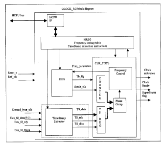
The system of the present invention, described herein as the clock rg circuit,
is shown in Fig. 1, and is constructed from two major blocks: the timestamp
extractor and the
clock controller. The block has two modes of operation: basestation and
terminal. In the
basestation mode, the circuit generates a local reference clock and a
timestamp for the
terminals. In the terminal mode, the circuit recovers the timestamp from the
data stream,
-2-
CA 02301436 2000-03-20
which it uses to synchronize a local DDS clock.
The timestamp extractor circuit parses the incoming data stream and extracts
the embedded timestamp. The circuit is based on a programmable byte processor.
The user
program the circuit with byte manipulation instructions that extract the
timestamp depending
on the data stream protocol ex: SES-Astra or DOCSIS.
The circuit is activated by the frame sync flag, which indicates the start of
an
extraction program. The circuit then runs until the end of its instruction
sequence, where it
halts until the next frame sync flag. The timestamp extracted can be up to 6
bytes long.
To accommodate DOCSIS, a CRC-CCITT 16 and a CRC-CCITT 32 circuit
are incorporated into the Timestamp Extractor block which treats parallel
data.
The timestamp extractor is sequenced by the byte arnval times. Since there is
no guaranteed minimum gap between successive bytes, it is therefore required
to perform all
parsing operations to be executed in 1 clock cycle. To achieve this, the
timestamp extractor
performs all branch, store and CRC operations in parallel. The defined
instruction word is 64
bits wide and is stored in a register space to provide 32 instructions. The
SES-Astra program
requires 11 instructions and DOCSIS, 20 instructions.
Once a timestamp is recovered from the incoming data stream a flag is set and
the timestamp is presented to the Clock Control block.
The clock controller operates in to modes: basestation or terminal. In the
basestation mode it is programmed to generate a reference clock and from the
same clock, a
timestamp. In the terminal mode, the circuit is programmed to synchronize a
local DDS clock
to the basestation reference clock. The synchronization method is based on
comparing the
local timestamp with the one sent by the basestation. The clock control block
also generates
the superframe pulse.
The HCPU is the control interface block, which is slaved to the ASIC's
860/8260
CPU interface block.
The HREG block contains the registers shared between the HCPU for
programming and the engine blocks for operation control. It is detached from
the HCPU because
it is part of the respective engine's clock domain.
The TimeStamp Extractor block is activated for the terminal mode. Its main
function is to recover the protocol dependent timestamp from the downstream
data. The block
-3-
CA 02301436 2000-03-20
is configured for a particular protocol operation via the HCPU register
settings. After
initialization, the block executes the programmed extraction algorithm block
every time the
frame sync is activated. If a timestamp is found, its value is loaded into the
TS register and the
block then idles until the next frame sync.
The DDS Clock is a direct digital synthesis clock circuit. This engine runs
off a
high-speed clock reference in order to synthesize a lower but variable
frequency.
The Clock Control is the main control engine. This block performs the
following
functions. Implements a protocol dependent timing recovery algorithm in the
terminal station
mode. Provides an accurate time base for base station mode. Locks on and track
to an upstream
clock reference. Controls the frequency selection of the DDS. Controls the
resetting of the DDS
TS counter. Filters out erroneous timestamps. Monitors the timestamp arrival
times.
Synchronizes the timestamp values, which are generated from 2 asynchronous
clocks.
Fig. 2 is a block diagram of the DDS block with signal inputs and outputs, as
detailed in the following list.
Ref clk: INPUT Clock that operates the FSM and is used as the
reference for the synthesized output clock.
dds_en: INPUT. DDS FSM enable; reset and operation control.
dds_load: INPUT DDS frequencey parameter load control. When
asserted, DDS will wait until current clock cycle
is complete then will restart FSM with new
frequency parameters.
dds clk:OUTPUT. Synthesized clock output
dds tb OUTPUT. DDS timebase flag. Asserted when
flg: all parameters
have been counted down to zero.
dds en: INPUT. FSM enable; reset and operation
control.
S1 cnt: INPUT. Sub loop count frequency parameter.
S1 np INPUT. Sub loop nominal period count frequency
cnt:
parameter.
S1 wf type: INPUT. Sub loop waveform type frequency parameter.
end_np cnt: INPUT. Timebase end nominal period count frequency
parameter.
-4-
CA 02301436 2000-03-20
To construct a nominal 27mhz with a 50% duty cycle clock from a higher
system clock requires a binary multiple: 54, 108, 216, etc. For physical ASIC
considerations
and for resolution requirements, the 108mhz frequency is chosen (assuming that
the duty
cycle variation is acceptable). The types of possible waveforms are shown in
Fig. 3.
By combining a sequence of nominal with either a short or long waveform, the
DDS can generate any frequency that varies in steps. For example, a sequence
of 269999982 NP
(nominal period) interspersed with 24 SP (short period) gives an average
frequency of 2700000.6
Hz over a duration of 10 sec. The resulting waveform sequence is shown in Fig.
4.
The DDS block is implemented with a look up table for the programmable
frequency values and a state machine to run the sequence based on a frequency
error input value.
The lookup table entry for one frequency setting is as shown in Fig. 5.
The TimeStamp Extractor block, shown in Fig. 6, is based on a CISC type
processor that executes user programmed instructions to parse through an
incoming data stream
and extract a timestamp value. The timestamp extractor's features: extracting
timestamp values
from incoming data stream; qualifying timestamp for clock control block; count
timestamp
extraction errors for SW diagnostics.
The Instruction Format for the TimeStamp Extractor (TSE) is shown in Appendix
C. The TSE operates on 2 main input streams: frame sync and data bytes that
arrive at the TSE's
clock rate; and RAM instructions.
The TSE is able to process the data on every clock. This constrains the
instruction
word format to be wide enough to describe all of the different types of
operations that occur in
parallel as demonstrated by the three pseudo code protocol algorithms
described at the end of this
document.
Fig. 7 shows the clock controller. The clock controller's features: detecting
loss
of timestamp for SW diagnostics; sets DDS's frequency under direct SW control,
automatically
varies DDS's clock frequency according to delta between local and extracted
timestamps.
The method of the present invention will now be described. In the SES-Astra
clock recovery mode:
SW enables and programs CLOCK RG for nominal frequency of 27Mhz. Clock
ready flag is off; hence TX mod is off.
SW enables RX demod to receive incoming data stream.
-S-
CA 02301436 2000-03-20
SW programs first PID value for timestamp extraction. If PCR PID is unknown,
SW can cycle through PID values until the prc rdy flag is set, indicating that
a possible
timestamp has been found. PCR value is accessible by SW. Its occurrence is
triggered by a
TS RDY interrupt.
CLOCK RG waits for 1 S' timestamp to preset internal counter and enable
counting. CLOCK RG uses the 27Mhz to increment the 42 bit counter where first
33 bits are in
units of 90Khz (base) and last 9 bits are remainder of 27Mhz divided by 300
(ext).
Upon arnval of 2°d timestamp, this value is compared to timestamp
generated via
internal clock programmed for 27Mhz. Delta instructs SW application, which
range of frequency
parameters to load into frequency selection table. Range is determined by on
board reference
clock uncertainty and specified system clock constraints: LTE 75 * 10**-3.
This gives .75 Hz
in 10 sec. Therefore a table of 32 values where each one has an accuracy of
.lHz provides 200
sec of automatic clock tracking before SW needs to update the frequency
parameter table. The
SW then sets CLOCK RG for tracking mode.
When DDS reaches end of frequency timebase (10 sec) it flags the CLOCK RG.
The following is rdy signal resets the DDS for phase and new frequency table
based on last valid PCR timestamp delta. The internal counter is updated with
this timestamp.
If this PCR is invalid (out of range due to bit error or discontinuity flag
set), CLOCK RG waits
for next PCR. This loop repeats until either a valid PCR is received or number
of invalid PCRs
sets interrupt for loss of sync.
CLOCK RG asserts the superframe flag every time it receives is rdy.
CLOCK RG in tracking mode compares the internal timestamp with the
recovered value. It then performs the following based on the difference:
Base delta = 0 (delta due to base station frequency variation specification)
Ext delta 0 = Frequency lock.
Ext delta 1,2 = Frequency lock. Index to next or .second next frequency
parameters in table and reset timestamp value. If index not in able, then
interrupt SW for new
frequency parameter table.
Ext delta > 2 = ignored on first and second occurrence, it is assumed that the
PCR
is in error, set SW interrupt to record event. On third occurrence, CLOCK RG
operation is reset
via SW.
-6-
CA 02301436 2000-03-20
Base delta > 0 = ignored on first and second occurrence, it is assumed that
the
PCR is in error, interrupt is set for SW to record event. On third occurrence,
CLOCK RG
operation is reset via SW.
CLOCK RG sets SW interrupt and resets clock rdy when it detects more than
3 consecutive discontinuity indicator flags.
CLOCK RG sets SW interrupt and resets clock rdy when it detects a 600msec
period with no PCR TS.
In clock generation mode: SW enables and programs CLOCK RG's DDS for
nominal frequency of 27Mhz. Clock ready flag is on.
CLOCK RG uses the 27Mhz to increment the 42 bit counter where first 33 bits
are in units of 90Khz and last 9 bits are remainder of 27Mhz divided by 300.
SW programs and enables the superframe counter to generate the SuperFrame
pulse.
In DOCSIS (clock recovery mode): SW enables and programs CLOCK RG for
nominal frequency of 10.24Mhz. Clock ready flag is off; hence TX mod is off.
SW enables RX demod to receive incoming data stream.
SW programs PID (1FFE) value for timestamp extraction. CMTS timestamp value
is accessible by SW. Its occurrence is triggered by a TS RDY interrupt.
CLOCK RG waits for 1 S' timestamp to preset internal counter and enable
counting.
Upon arnval of 2°d timestamp (200ms later), this value is compared to
timestamp
generated via internal clock programmed for 10.24Mhz. Delta instructs SW
application, which
range of frequency parameters to load into frequency selection table. Range is
determined by on
board reference clock uncertainty and specified system clock constraints:
constraints lOns fitter
and 10**-8 drift rate = duration of adjacent 102,400,000 segments within LTE
120ns. This gives
1.2 Hz in 10 sec. Therefore a table of 24 values where each one has an
accuracy of .lHz is
required. The SW then sets CLOCK RG for tracking mode.
When DDS reaches end of frequency timebase (10 sec) it flags the CLOCK RG.
The following is rdy signal resets the DDS for phase and new frequency table
based on last valid
CMTS timestamp delta. The internal counter is updated with this timestamp. If
this CMTS is
invalid (out of range due to bit error or transport_error indicator set),
CLOCK RG waits for next
_7_
CA 02301436 2000-03-20
CMTS. This loop repeats until either a valid CMTS is received or number of
invalid CMTS sets
an interrupt for loss of sync.
CLOCK RG asserts the superframe flag every time it receives is rdy.
CLOCK RG in tracking mode compares the internal timestamp with the
recovered value. It then performs the following based on the difference:
Delta 0 = Frequency lock.
Delta 1,2 = Frequency lock. Index to next or second next frequency parameters
in table and reset timestamp value. If index not in table, then interrupt SW
for new frequency
parameter table.
Delta > 2 = ignored on first and second occurrence, it is assumed that the PCR
is
in error, set SW interrupt to record event. On third occurrence, CLOCK RG
operation is reset
via SW.
CLOCK RG sets SW interrupt and resets clock rdy when it detects more than
3 consecutive transport-error indicator flags.
CLOCK RG sets SW interrupt and resets clock rdy when it detects a 600msec
period with no CMTS TS.
In clock generation mode: SW enables and programs CLOCK RG's DDS for
nominal frequency of 10.24Mhz. Clock ready flag is on.
CLOCK RG uses the 10.24Mhz to increment the 32 bit timestamp counter.
Advantages of the present invention include the following features: user
programmability for timestamp extraction algorithms, protocol based timestamp
generation for
base stations, protocol based timestamp extraction for terminal stations,
clock recovery for
terminal stations, SuperFrame generation and detection, and DDS clock with a
resolution of .lHz
Fig. 8 shows the TS XTRACTR to CLOCK CNTL handoff circuit.
The above-described embodiments of the invention are intended to be examples
of the present invention. Alterations, modifications and variations may be
effected the particular
embodiments by those of skill in the art, without departing from the scope of
the invention which
is defined solely by the claims appended hereto.
_g_
CA 02301436 2000-03-20
SES-Astra Table:
Frequency SubLoop # Nominal num End Period End numberTimebase
Type Frequency
27 Mhz + 10 4 674998 SP 5 100 msec
27 Mhz + 810 324 8332 SP 189 100 msec
27 Mhz + 200 80 33748 SP 100 100 msec
27 Mhz + 100 40 67498 SP 50 100 msec
27 Mhz + .1 4 67499998 SP 5 10 sec
27 Mhz 100 2699999 NP 0 10 sec
27 Mhz - .1 4 67499997 LP 7 10 sec
27 Mhz - 100 40 67498 LP 70 I 00 msec
27 Mhz -200 80 33748 LP 140 100 msec
27 Mhz - 810 324 8332 LP 27 100 msec
27 Mhz - 1 4 6749997 LP 7 ~ 1 sec
Base station accuracy 27Mhz +/- 810hz, rate of change =< 75 * 10 ** -3hz/sec
(in 10 sec = .75hz)
Therefore, the expected change in frequency is less than .1 hz.
Table calculations:
1 fsm clock cycle @ 108Mhz = 9.26ns => in 10 sec = 1080000000 fsm cycles
1 PCR clock cycle @ 27Mhz = 37ns => in 10 sec = 270000000 PCR clock cycles
Number of nominal PCR clock cycles = X, number of short PCR clock cycles = Y
and long = Z
Equation 1: center frequency
X*4 = 108000000 and X = 27000000 or 10000 sub loops of 2699 NP + 1 NP
Equation 2: > center frequency
X*4 + Y*3 = 108000000 and X + Y = 27000000 + delta
Equation 3: < center frequency
X*4 + Z*5 = 108000000 and X + Z = 27000000 - delta
init PCR 1 Timebase PCR 2
Local 1 Local 2
Error = (local2 -PCR2)/ ((local2 -locally/ local freq) = delta of counts for
time period between PCR1 and PCR2
Approximation: timebase is 10 sec for .Ihz accuracy and timebase to PCR2 is
usually <.lsec =>
Error ~ (local2 -PCR2)/ 10
CA 02301436 2000-03-20
DOCSIS Table:
Frequency SubLoop # Nominal num End Period End numberTimebase
Type frequency
10.24 Mhz 2048 49998 SP 2560 10 sec
+ 51.2
10.24 Mhz 556 184170 SP 229 10 sec
+ 13.9
10.24 Mhz 40 67498 SP 50 10 sec
+ 10
10.24 Mhz 4 25599998 SP 5 10 sec
+ .1
10.24 Mhz 100 10239 NP 0 100 msec
10.24 Mhz 4 25599997 LP 7 10 sec
- .1
10.24 Nihz 4 2559997 LP 7 1 sec
- 1
10.24 Mhz 4 255997 LP 7 100 msec
- 10
10.24 Mhz 2048 49997 LP 1536 10 sec
- 51.2
Table calculations:
Base station accuracy +/- 5 ppm = 10.24 Mhz +/- 51.2 Hz. Drift rate =< 10 * *-
8 per second ( 10 nsec per sec)
Therefore, the expected change in frequency is equal to .1 hz.
1 fsm clock cycle @ 40.96Mhz = 24.4ns => in 10 sec = 409600000 fsm cycles
1 DDS clock cycle @ 10.24Mhz = 97.66ns => in 10 sec = 102400000 dds clock
cycles
Number of nominal period clock cycles = X, number of short period clock cycles
= Y and long = Z
Equation 1: center frequency
X*4 = 409600000 and X = 102400000 or 10000 sub loops of 102399 NP + 1 NP
Equation 2: > center frequency
X*4 + Y*3 = 409600000 and X + Y = 102400000 + delta
Equation 3: < center frequency
X*4 + Z*5 = 409600000 and X + Z = 102400000 - delta
CA 02301436 2000-03-20
HCS control RSVD Data RSVD Instruction
instructions control branch
instructions control
63:60 59 58:40 39: 35 34:0
Instruction
branch
control
34:31 30:28 27:20 19:12 11:6 5:0
InstructionSowce Mask Compare True False case:
Data case:
opcode select operand operand 6 6 bit Ram branch
bit faddy
Ram
branch
taddr
Branch control instruction list:
0: BNOP: wait for frame sync to restart
1: JMP: goto [faddy]
2: JEQ: if { ([data] AND [mask op]) then goto [faddy] else goto
_ [comp op]} [faddy]
3; JGT: if { ([data] AND [mask op]) then goto [faddy] else goto
> [comp op]} [faddy]
4: JLT: if { ([data] AND [mask op]) then goto [faddy] else goto
< [comp opJ} [faddy]
5: ]DBE: if { ([dbyte] AND [mask op])then goto [faddy] else dec [dbyteJ
_ [comp op]} and goto [faddy]
6: JDWE: if { [dword] _ [mask op]
&[comp op]} then goto [faddy]
else dec [dword] and goto[faddy]
7: JHCSOEQ:if { ([data] XOR [mask op]) then goto [faddy] else goto
= HCS[7:OJ} [faddy]
8: JHCS1EQ:if { ([data] XOR [mask op]) then goto [faddy] else goto
= HCS[15:8]} [faddy]
9: JMCSOEQ:if { ([data] XOR [mask op]) then goto [faddy] else goto
= CRC[7:0]} [faddy]
a: JMCS1EQ:if { ([data] XOR [mask op]) then goto [faddy] else goto
= CRC[15:8]} [faddy]
b: JMCS2EQ:if { ([data] XOR [mask op]) then goto [faddy] else goto
= CRC[23:16]} [faddy]
c: JMCS3EQ:if { ([data] XOR [mask op]) then goto [faddy] else goto
= CRC[31:24]} [faddy]
JEQ,
JGT,
LPB,
JHSCEQ:
sowce
data
select
000 Input
byte
001 Byte reg-1
010 Byte reg
2
011 Byte reg
3
100 Byte reg
4
101 DB reg
0
110 DW reg_1
111 DW reg
2
CA 02301436 2000-03-20
Data control Data Inst ion Data
17:0 Destinat decode
18:16 (58:56)15:13 (55:53) 12:5 4:0 (44:40) 00000 X
(52:45)
Opcode Source Data selectMask/data Destination 00001
Byte reg-1
Data
d
operan
00010 Byte reg
2
Instruction 00011 Byte reg
list: 3
1- 000: 00100 B a re 4
DNOP: ~ - g-
no operation
2- 001:
DSMD:
([source
data]
AND [mask
op]) _>
[dest.
data]
3- 010: 00101 DB reg
DIMD:
[mask
op] _>
[dest.
data]
RDY
(0)] _>
TS
set [mask
o
if t
e fla
DTTSRDY
O 11
4
_ 00110 DW reg L
p )
ru
g
:
:
-
5- 100:
DREGADD:
([source
data]
+ [mask
op]) _>
[dest.
data]
t
d
t
d
k
_>
. 00111 DW reg M
a - -
a
es
op])
[
6- 101:
DREGSUB:
([source
data]
- [mas
I 10: DDWINC:
DW + 1
=> DW
7-
8- 111:
DDWDEC: 01000 HCS SEEDO
DW - 1
=> DW
01001 HCS SEED1
01010 MCS SEEDO
01011 MCS SEED1
01100 MCS SEED2
01101 MCS SEED3
01110 TS RDY
01111 rsvd
10000 TS reg-1
10001 TS reg 2
10010 TS reg 3
10011 TS reg 4
10100 TS reg 5
10101 TS reg_6
Instruction
list:
1- 0000: CNOP:
2- 0001: LDHCS: [Input byte]
_> HCS
3- 0010: TFHCS:if true [Input byte]
flag set _> HCS
4- 0011: FFHCS:if false [Input byte]
flag set _> HCS
CRC control 5- 0100: LDMCS: [Input byte]
_> MCS
6- OlOI:TFMCS:if true [Input byte]
flag set _> MCS
3:0 (63:60) 7- O1 lO:FFMCS:if false [Input byte]
flag set _> MCS
8 0111 0000 => HCS
RHCS
- . :
:
Instruction 9- 1000: PHCS: FFFF => HCS
oocode 10- 1001: RMCS: 00000000 =>
MCS
11- 1010: PMCS: FFFFFFF =>
MCS
12- 1011: RHMCS:RHCS and
RMCS
13- 1100: PHMCS:PHCS and
PMCS
STOR source
data
select
decode
000 Input
byte
001 Byte reg_1
010 Byte reg
2
011 Byte reg_3
100 Byte reg
4
101 DB reg
110 DW reg
L
111 DW reg
M
CA 02301436 2000-03-20
SES ASTRA:
SES Astra or ITU-T H.222.0 timesamp extraction algorithm: (instructions are
not executed until byte rdy
occurs). Timestamp arrives every 100 cosec or less. Loss of timestamp for *?*
cosec causes TX shutdown.
Frame sync flag~Reset FSM and registers. Goto stepl /* flag qualifies MPEG
SYNC = 47 */
1- if byte( 7) = 0 TEI and byte(4:0) = PID msb then
goto step 2 /* PID msb match */
else
Goto idle state and wait for frame start
2- if byte(7:0) = PID lsb then
goto step 3 /* PID lsb match */
else
Goto idle state and wait for frame start
3- if byte(5) = 1 AFC lsb then /* mask in AFC bit */
goto step 4 /* AFC match *1
else
Goto idle state and wait for frame start
4- If byte > 6 then /* check adaption field length for PCR */
Goto step 5 /* PCR minimum length ok */
Else
Goto idle state and wait for frame start
5- If byte(7) = 0 and byte(5) = 1 then /* discontinuity error not set and PCR
ok */
Goto step 6
Else
Goto idle state and wait for frame start /* PCR discontinuity or no PCR */
6- Store PCR(47:40)
7- Store PCR(39:32)
8- Store PCR(31:24)
9- Store PCR(23:16)
10- Store PCR(15:8)
11- Store PCR(7:0) and set timestamp flag + Goto idle state and wait for frame
start
CA 02301436 2000-03-20
DOCSIS protocol:
Docsis timesamp extraction algorithm: (instructions are not executed until
byte rdy occurs)
Timestamp arrives every 200 cosec. Loss of timestamp for 600 cosec causes TX
shutdown.
Frame sync flag~Reset FSM and registers. Goto stepl /* flag qualifies MPEG
SYNC = 47 */
1- if TEI bit 7 in byte = 0 and PUSI bit 6 in byte = 1 and byte(4:0) = PID msb
then
goto step 2 /* PID msb match */
else
Goto idle state and wait for
frame start
2- if byte(7:0) = P)D lsb then
goto step 3 /* P)D lsb match */
else
Goto idle state and wait for
frame start
3- goto step 4 /* ignore AFC */
4- If byte = 0 then /* check pointer field */
Goto step 5
Else
goto step 6
store byte in Dbyte /* save pointer_field in decrement
byte reg*/
Preset HCS and MCS
5- If byte = ff then /* if stuff bytes then filter
*/
goto 5 (set true flag) /* loop while ff */
Else
Goto 7 (set false flag)
If false flag set then
Enable HCS on byte
Store byte in TempReg (FC byte)
6- If DByte = 0 then /* pointer field = MAC tail filter */
goto 5
Else
Decrement Dbyte: goto 6 /* loop until end of MAC tail */
7- If TempReg (7:6) = Mac specific Header and TempReg (5:1 ) = Timing Header
and TempReg (0) = 0 then
goto step 8 /* Timing MAC header match */
Else
Goto step 42 /* non Timing MAC header filter */
Enable HCS on byte /* perform HCS on Mac_parm */
CA 02301436 2000-03-20
8- Store byte in TempWord(15:8) (length msb)
Enable HCS on byte
9- Store byte in TempWord(7:0) (length lsb)
Enable HCS on byte
10- if byte = !HCS msb then
goto step 11 /* HCS msb match */
else
Goto idle state and wait for frame start /* bad CRC wait for next frame */
11- if byte = !HCS lsb then
goto step 12 /* HCS msb match */
else
Goto idle state and wait for frame start /* bad CRC wait for next frame */
Preset HCS
12- Enable MCS on byte; goto /* MCS on DA(23:16) */
next step
13- Enable MCS on byte; goto /* MCS on DA(15:8) */
next step
14- Enable MCS on byte; goto /* MCS on DA(7:0) */
next step
15- Enable MCS on byte; goto /* MCS on SA(23:16) */
next step
16- Enable MCS on byte; goto /* MCS on SA( 15:8) */
next step
17- Enable MCS on byte; goto /* MCS on SA(7:0) */
next step
18- Enable MCS on byte; goto /* MCS on LEN msb */
next step
Store byte in DWord /* keep length in case wrong
Mac msg */
19- Enable MCS on byte; goto /* MCS on LEN lsb */
next step
Store byte in Dword /* keep length in case wrong
Mac msg *l
20- Enable MCS on byte; goto /* MCS on DSAP */
next step
Decrement DWord
21- Enable MCS on byte; goto /* MCS on SSAP */
next step
Decrement DWord
22- Enable MCS on byte; goto /* MCS on SSAP */
next step
Decrement DWord
23- Enable MCS on byte; goto /* MCS on Control */
next step
Decrement DWord
24- if byte = 1 then /* check version */
goto 25
else
goto 37
Decrement DWord
Enable MCS on byte
25- if byte = 1 then /* check type */
goto 26
else
goto 37
Decrement DWord
Enable MCS on byte
26-Enable MCS on byte /* MCS on RSVD */
Decrement DWord
CA 02301436 2000-03-20
27- if Dword = 9 then /* check last byte before
CMTS */
goto 28
else
goto 27 /* loop until end */
Decrement DWord
Enable MCS on byte
28- Store CMTS(31:24)
Enable MCS on byte
29- Store CMTS(23:16)
Enable MCS on byte
30- Store CMTS(15:8)
Enable MCS on byte
31- Store CMTS(7:0)
Enable MCS on byte
32- if byte = !MCS(31:24) then/* check CRC */
.
goto 33
else
Goto idle state and wait for /* bad MCRC wait for next
frame start frame */
33- if byte = !MCS(23:16) then/* check CRC */
goto 34
else
Goto idle state and wait for /* bad MCRC wait for next
frame start frame */
34- if byte = !MCS(15:8) then /* check CRC */
goto 35
else
Goto idle state and wait for /* bad MCRC wait for next
frame start frame */
35- if byte = !MCS(7:0) then /* check CRC */
Goto idle state and wait for
frame start
else
Goto idle state and wait for /* bad MCRC wait for next
frame start frame */
If true flag set then
Set TS RDY
CA 02301436 2000-03-20
36- if Dword = 5 then /* check last byte before
CRC */
goto 37
else
goto 36 /* loop until end */
Decrement DWord
Enable MCS on byte
38- if byte = !MCS(31:24) /* check CRC */
then
goto 39
else
Goto idle state and wait /* bad MCRC wait for next
for frame start frame */
39- if byte = !MCS(23:16) /* check CRC */
then
goto 40
else
Goto idle state and wait /* bad MCRC wait for next
for frame start frame */
40- if byte = ~MCS(15:8) /* check CRC */
then
goto 41
else
Goto idle state and wait /* bad MCRC wait for next
for frame start frame */
41- if byte = !MCS(7:0) /* check CRC */
then
goto 4 /* go to next mac message
*/
else
Goto idle state and wait /* bad MCRC wait for next
for frame start frame */
Preset HCS
/* wrong FC message */
42- Store byte in DWord(15:8)
(length msb)
Enable HCS on byte /* enable HCS on LEN msb
*/
43- Store byte in DWord(7:0)
(length Isb)
Enable HCS on byte
44- if byte = !HCS msb then
goto step 45 /* HCS msb match */
else
Goto idle state and wait /* bad CRC wait for next
for frame start frame */
45- if byte = !HCS lsb then
goto step 46 /* HCS msb match */
else
Goto idle state and wait /* bad CRC wait for next
for frame start frame */
46- If DWord = 0 then /* loop until end of MAC
frame */
Goto step 4 /* goto stuff byte check
*/
Else
Decrement TempWord
CA 02301436 2000-03-20
SES-ASTRA timestamp instruction program
AddrHCS Data op Branch taddr faddy
op op
00- CNOP DNOP [X] [X] JEQ [000] [pid [O1 [Oc]
[X] [9f] msb] ]
O1- CNOP DNOP [X] [X] JEQ [000] [pid [02] [Oc]
[X] [ff] lsb]
02- CNOP DNOP [X] [X] JEQ [000] [acfJ [03] [Oc]
[X] [20]
03- CNOP DNOP [X] [X] JGT [000] [07] [04] [Oc]
[X] [ffJ
04- CNOP DNOP [X] [X] JEQ [000] [10] [OS] [Oc]
[X] [90]
OS- CNOP DSMD [000] [ff]JMP [X] [X] [06] [X]
[15] [X]
06- CNOP DSMD [000] [ff]JMP [X] [X] [07] [X]
[14] [X]
07- CHOP DSMD [000] [ffJJMP [X] [X] [08] [X]
[13] [X]
08- CNOP DSMD [000] [ff]JMP [X] [X] [09] [X]
[12] [X]
09- CNOP DSMD [000] [ff]JMP [X] [X] [Oa] [X]
[11] [X]
Oa- CNOP DSMD [000] [ff]JMP [X] [X] [Ob] [X]
[10] [X]
Ob- CNOP DIMD [X] [O1] JMP [X] [X] [Oc] [X]
[Oe] [X]
Oc- CNOP DIMD [X] [00] JMP [X] [X] [Oc] [X]
[Oe] [X]
constant astrax_code_0 : X"0000 0001 09f1 a04c";
constant astrax_code_1 : X"0000 0001 Off6 908c ";
constant astrax_code_2 : X"0000 0001 0202 OOcc ";
constant astrax_code_3 : X"0000 0001 8ffU 710c";
constant astrax_code_4 : X"0000 0001 0901 014c";
constant astrax_code_5 : X"O1 if f500 8000 0180";
constant astrax_code_6 : X"O1 if f400 8000 OlcO";
constant astrax_code_7 : X"O1 if f300 8000 0200";
constant astrax_code_8 : X"O1 if f200 8000 0240";
constant astrax_code_9 : X"O1 if f100 8000 0280";
constant astrax_code_10 : X"O1 if fU00 8000 02c0";
constant astrax_code_l l : X"0200 2e00 8000 0300";
constant astrax code 12 : X"0200 Oe00 8000 0300";
Example for extracting 4 extra bytes after timestamp:
constant astra_code_0X"0000 0001 09f1
: a050";
code X"0000 0001 Off6
1 : 9090 ";
constant astra
_ X"0000 0001 0202
_ OOdO ";
constant astra_code_2
:
constant astra_code_3X"0000 0001 8ffl~
: 7110";
constant astra_code_4X"0000 0001 0901
: 0150";
constant astra_code_5X"011 f f500
: 8000 0180";
constant astra_code_6X"O1 if f400
: 8000 OlcO";
constant astra_code_7X"O1 if f300
: 8000 0200";
constant astra_code_8X"011 f f200
: 8000 0240";
constant astra_code_9X"O1 if f100
: 8000 0280";
code_10 : X"Ol if ft700
constant astra 8000 02c0";
_ X"011 f e400
constant astra_code_l8000 0300";
l :
12 : X"Ol if e300
code 8000 0340";
constant astra
_ X"O1 if e200
_ 8000 0380";
code_13 :
constant astra
_ X"O1 if e100
constant astra_code_148000 03c0";
:
code X"0200 2e00 8000
15 : 0400";
constant astra
_ X"0200 Oe00 8000
_ 0400";
constant astra
code 16 :
CA 02301436 2000-03-20
DOCSlS timestamp instruction program
AddrHCS Data Branch taddr faddy
op op op
00- CHOP DNOP [X] [X] JEQ [000] [pid [01 (
[X] [df] msb] ] 12]
O1- CNOP DNOP [XJ [X] JEQ [000] [pid [02] (12]
[X] [ffJ lsb]
02- CNOP DNOP [X] [X] JMP [X] [X] [03] [X]
[X] [X]
03- PHMCS DSMD [000] JEQ [000] [00] [04] [OS]
[ffJ [ffJ
[OS]
04- FFHCS DSMD [000] JEQ [000] [ffJ [04] [06]
[ffJ [ffJ
[Oi]
OS- CNOP DSMD [000] JDBE [000] [00] [04] [OS]
[ffJ [ff]
[10]
06- LDHCS DNOP [X] [X] JEQ [001] [c0] [07] [28]
[X] [ff]
07- LDHCS DNOP [X] [X] JMP [X] [X] [08] [X]
[X] [X]
08- LDHCS DNOP [X] [X] JMP [X] [X] [09] [X]
[X] [X]
09- CNOP DNOP [X] [X] JHCS1EQ [000] [X] [Oa] [2e]
[X] [ffJ
Oa- CNOP DNOP [X) [XJ JHCSOEQ [OOOJ [X] [ObJ [2e]
[X] [ffJ
Ob- LDMCS DNOP [X] [X] JMP [X] (X] [Oc] [X]
[X] [X]
Oc- LDMCS DNOP [X] [X] JMP [X] [X] [Od] [X]
[XJ [X]
Od- LDMCS DNOP [X] [X] JMP [X] [X] [OeJ [X]
[X] [X]
Oe- LDMCS DNOP [X] [X] JMP [X] [X] [OfJ [X]
[X] [XJ
Of LDMCS DNOP [X] [X] JMP [X] [X] [lOJ [X]
[X] [X]
10- LDMCS DNOP [X] [X] JMP [X] [X] [ 11 [X]
[X] [X] ]
11- LDMCS DSMD [000] JMP [X] [X] [12] [X]
[ffJ [X]
[07]
12- LDMCS DSMD [000] JMP [X] [XJ [13] [X]
[ffJ [X]
[06]
13- LDMCS DDWDEC [X] [X] JMP [X] [X] [14] [X)
[X] [X]
14- LDMCS DDWDEC [X] [X] JMP [X] [X] [15] [X]
[X] [X]
15- LDMCS DDWDEC [X] [X] JMP [X] [X] [16] [X]
[X] [X]
16- LDMCS DDWDEC [X] [X] JMP [X] [X] [17] [X]
[X] [X]
17- LDMCS DDWDEC [X] [X] JEQ [000] [O1] [18] [28J
[X] [ffJ
18- LDMCS DDWDEC [X] [X] JEQ [000] [O1] [19] [28]
[X] [ffJ
19- LDMCS DDWDEC [X] [X] JMP [X] [X] [la] [X]
[X] [X]
la- LDMCS DNOP [X] [X] JDWE [000] [09] [lb] [la]
[XJ [ffJ
lb- LDMCS DSMD [000] JMP [X] [X] [lc] [X]
[ffJ [XJ
[13]
lc- LDMCS DSMD [000] JMP (X] [X) [ld] [X]
[ffJ [X]
[12]
ld- LDMCS DSMD [000] JMP [X] [X] [le] [X]
[ffJ [X]
[11]
1 LDMCS DSMD [000] JMP [X] ~ [X] [ 1 [X]
e- [ffJ [X] fJ
[ 10]
1f CNOP DNOP [XJ [X] JMCS3EQ [000] [X] [20] [2e]
[X] [ff]
20- CNOP DNOP [X] [X] JMCS2EQ [000] [X] [21 [2e]
[X] [ffJ ]
21- CNOP DNOP [X] [X] JMCS1EQ [000] [X] [22] [2e]
[X] [ff]
22- CNOP DTTSRDY[X] [O1] JMCSOEQ [000] [X] [2e] [2e]
[X] [ffJ
23- LDMCS DDWDEC [X] [X] JDWE [000] [5] [24] [23]
[X] [ffJ
24- CNOP DNOP [X] [X] JMCS3EQ [000] [X] [25] [2e]
[X] [ff]
25- CNOP DNOP [X] [X] JMCS2EQ [000] [X] [26J [2e]
[X] [ffJ
26- CNOP DNOP [X] [X] JMCS1EQ [000] [X] [27] [2e]
[X] [ffJ
27- CNOP DNOP (X) [X] JMCSOEQ [000] [XJ [04] [2e]
[X] [ffJ
28- LDHCS DSMD [000] JMP [X] [X] [29] [X]
(ff] [X]
[07]
29- LDHCS DSMD [000] JMP [X] [X] [2a] [X]
[ff] [X]
[06]
2a- CNOP DNOP [X] [X] JHCS1EQ [000] [X] [2b] [2e]
[X] [ffJ
2b- CNOP DNOP [X] [X] JHCSOEQ [000] [X] [2c] [2e]
[X] [ffJ
2c- LDMCS DNOP [X] [X] JDWE [000] [00] [04) [2c]
[X] [ffJ
2d- CNOP DNOP [X] [X] BNOP [X] [X] [XJ [X]
[X] [X]
CA 02301436 2000-03-20
Register List:
Timestamp extractor:
# timestamp extractor register set
DEVICE_ID = 6'd34;
DEVICE NAME = "cpu is xtrctr";
# block enable register
# bit 0 is xtrctr
REGISTER ARRAY l:
TITLE = "timestamp extraction control";
NAME = "control";
DEFAULT = 1'h0;
ATTR = R/W;
END;
# timestamp extraction program registers
# 64 locations for DOCSIS
REGISTER ARRAY 64:
TITLE = "timestamp extraction program instructions";
NAME = "tsx code";
DEFAULT = 64'h0;
ATTR = R/W;
END;
# SW access points
# status input to HREG
# bit 0 ts_rdy
# bit 1 HCS error
# bit 2 MCS error
REGISTER:
TITLE = "ts status bits";
NAME = "ts status";
DEFAULT = 3'h0;
ATTR = R/E;
END;
# recovered data
REGISTER:
TITLE = " timestamp data lsb";
NAME = "ts reg 4 1";
DEFAULT = 32'h0;
ATTR = R/E;
END;
CA 02301436 2000-03-20
REGISTER:
TITLE = " timestamp data msb";
NAME = "ts reg 6 5";
DEFAULT = 16'h0;
ATTR = R/E;
END;
REGISTER:
TITLE = " general purpose registers";
NAME = "gen byte-4-1";
DEFAULT = 32'h0;
ATTR = R/E;
END;
CA 02301436 2000-03-20
Clock recovery and generation:
# k recovery and ation register set
Cloc gener
DEVICEID = 5'd29;
DEVICE_ cntl";
_NAME = "cpu is
clk-
# access diag register
cpu
REGISTER:
TITLE = "cpu accessID reg";
NAME = "blkid";
DEFAULT = 16'h0;
ATTR = R/E;
END;
# k enable register
bloc
# cntl enable the clock control block
bit en .
clk
0 ts
# _ enable auto mode for clock control
bit _ block
_
en .
clk
auto
1 ts
# _ window timebase counter enable
bit _
_
en .
2 wtb
count
# _ superframe block enable
bit _
en .
3 sf
cntl
# _ superframe block rx/tx recover or
bit _ generate
4 sf
mode .
mode _
# ld . superframe timestamp load control
bit 5 sf
ts
# _ timestamp SES/DOCSIS type
bit _
type .
6 ts
# _ enable the DDS block
bit en .
7 dds
# _ force clock lock
bit lock
cntl :
8 clock
# _ load timestamp
bit _
load .
9 swts
# _ load increment timestamp
bit 10 swts inc load
.
REGISTER:
TITLE = "clock
recovery and
generation control";
NAME = "control";
DEFAULT = 11'h0;
ATTR = R/W;
END;
# us input to HREG
stat
# tb_flg . DDS timebase flag
bit 0 dds
# _ loss of timestamp flag
bit flg .
1 ts
loss
# _ frequency parameter table update
bit _ attention
2 fp_attn-flg
.
flag
# 3 ts_rdy_reg . timestamp data and counter ready
bit
# err . timestamp delta range error
bit delta
4 ts
# _ frequency parameter table overflow
bit _ error
err .
of
5 fp
tbl
# _ frequency parameter table underflow
bit _ error
_
err .
tbl
uf
6 fp
# _ clock lock indicator
bit _
_
7 clock lock .
REGISTER:
TITLE = "clock
recovery and
generation status";
NAME = "status";
DEFAULT = 8'h0;
ATTR = R/E;
END;
CA 02301436 2000-03-20
# recovered timestamp loss threshold: ts_loss thrshld
REGISTER:
TITLE = "timestamp loss threshold";
NAME = "ts loss thrshld";
DEFAULT = 8'h0;
ATTR = R/W;
END;
# timestamp delta maximum filter
REGISTER:
TITLE = "timestamp delta max";
NAME = "ts delta max";
DEFAULT = 32'h0;
ATTR = R/W;
END;
# window timebase terminal count wtb_tc
REGISTER:
TITLE = "window timebase terminal count";
NAME = "wtb tc";
DEFAULT = 32'h0;
ATTR = R/W;
END;
# timestamp load value
REGISTER:
TITLE = " timestamp load lsb";
NAME = "swts field lsb";
DEFAULT = 32'h0;
ATTR = R/W;
END;
REGISTER:
TITLE = " timestamp load msb";
NAME = "swts field msb";
DEFAULT = 10'h0;
ATTR = R/W;
END;
# increment timestamp load value
REGISTER:
TITLE = " timestamp inc load lsb";
NAME = "swts inc field";
DEFAULT = 8'h0;
ATTR = R/W;
END;
# superframe timestamp compare value
REGISTER:
TITLE = " superframe timestamp lsb";
NAME = "sf is lsb";
DEFAULT = 32'h0;
ATTR = R/W;
END;
CA 02301436 2000-03-20
REGISTER:
TITLE = " superframe timestamp msb";
NAME = "sf is msb";
DEFAULT = 10'h0;
ATTR = R/W;
END;
# sf_tc_cnt -- superframe terminal count
REGISTER:
TITLE = " superframe generator terminal count";
NAME = "sf tc cnt";
DEFAULT = 32'h0;
ATTR = R/W;
END;
# tsd_field_lsb :access tsd read data for SW
# tsd field msb :access tsd read data for SW
REGISTER:
TITLE = " timestamp data lsb";
NAME = "tsd field lsb";
DEFAULT = 32'h0;
ATTR = R/E;
END;
REGISTER:
TITLE = " timestamp data msb";
NAME = "tsd field msb";
DEFAULT = 10'h0;
ATTR = R/E;
END;
# tsc_field_lsb :access local is counter read data for SW
# tsc field msb :access local is counter read data for SW
REGISTER:
TITLE = " timestamp count lsb";
NAME = "tsc field lsb";
DEFAULT = 32'h0;
ATTR = R/E;
END;
REGISTER:
TITLE = " timestamp count msb";
NAME = "tsc field msb";
DEFAULT = 10'h0;
ATTR = R/E;
END;
# frequency parameters
REGISTER ARRAY 16:
TITLE = "Freq parameter NP number per loop slow ";
NAME = "fp-lnp-s";
CA 02301436 2000-03-20
DEFAULT = 27'h0;
ATTR = R/W;
END;
REGISTER ARRAY 16:
TITLE = "Freq parameter loop number, loop type and NP number for
end sequence slow ";
NAME = "fp lte s";
DEFAULT = 25'h0;
ATTR = R/W;
END;
REGISTER:
TITLE = "Freq parameter NP number per loop nominal ";
NAME = "fp lnp n";
DEFAULT = 27'h0;
ATTR = R/W;
END;
# 27 Mhz value = 2932df
REGISTER:
TITLE = "Freq parameter loop number, loop type and NP number for
end sequence nominal ";
NAME = "fp lte n";
DEFAULT = 25'h0;
ATTR = R/W;
END;
# 27 Mhz value = 64
REGISTER ARRAY 15:
TITLE = "Freq parameter NP number per loop fast ";
NAME = "fp lnp f";
DEFAULT = 27'h0;
ATTR = R/W;
END;
REGISTER ARRAY 15:
TITLE = "Freq parameter loop number, loop type and NP number for
end sequence fast ";
NAME = "fp lte f";
DEFAULT = 25'h0;
ATTR = R/W;
END;