Note: Descriptions are shown in the official language in which they were submitted.
CA 02301615 2000-02-24
WO 99/13515 PCTIUS98/17999
INTEGRATED CIRCUIT PACKAGE EMPLOYING A TRANSPARENT
ENCAPSULANT AND A METHOD OF MAKING THE PACKAGE
5~ . __
FIELD OF THE INVENTION
The present invention relates to integrated
circuit packages, and in particular to a package for 'an
integrated circuit device having circuitry whose
functioning requires the transmission of light through
the package.
BACKGROUND OF THE INVENTION
Integrated circuits devices are typically housed
in packages. Typical packages are made of plastic,
ceramic, or metal. The packages include internal and
external conductive structures, such as metallized
vial, metal traces, bond wires, and solder
interconnection balls or leadless chip carrier ("LCC")
pads, for electrically connecting the integrated
circuit device in.the package to external circuitry,
such as a circuit board.
Certain types of integrated circuit devices, such
as erasable programmable read-only memory devices
("EPROM"), charge coupled devices ("CCD") or optical
sensing devices, such as those used in document
scanners, fingerprint recognition equipment, or other
consumer products, require a selected or continuous
transmission of light of a selected frequency through
the top surface of the package onto the surface of the
integrated circuit die within the package. Typically,
CA 02301615 2000-02-24
WO 99113515 PCT/US98117999
the packages for such integrated circuit devices have a
glass or quartz window in the otherwise opaque top
surface of the package. This transparent window is
located above the die, and the selected frequency of
light passes through the window and impinges on the top.__-
surface of the die. Unfortunately, packages having
such glass or quartz inserts are relatively expensive
to fabricate, which raises the cost of the products in
which the integrated circuit devices are used. A less
expensive alternative would have wide application.
SUMMARY OF INVENTION
Embodiments of an improved package for integrated
circuit devices, such as EPROM and CCD or other optical
devices whose functioning requires a selective or
continuous transmission of light through a portion of
the package, are disclosed. Exemplary methods of
making such packages are also described.
The package has a planar insulating substrate
base, which may be formed of an epoxy laminate or
ceramic. The substrate has a first surface and an
opposite second surface. Metallized vias extend
through the substrate. An integrated circuit die
having light-sensitive circuitry, such as a die for a
CCD device, is affixed to the first surface of the
substrate. Bond wires are installed which electrically
connect the conductive bonding pads on the die to
conductive structures on the first surface of the
substrate, such as metal traces and contact pads.
These conductive structures are in turn electrically
-2-
CA 02301615 2000-02-24
WO 99/135I5 PCT/US98117999
connected to the metallized vias through the substrate.
Conductive structures on the second surface of the
substrate,- such as solder interconnection balls or LCC
pads, -for connecting the package to external circuitry
are electrically connected to the metallized vias and _.-
hence to the die.
After the bond wires are installed, a bead of an
adhesive material such as epoxy plastic is deposited
onto the first surface of the substrate peripherally
around the die. The bead covers the peripheral side
surfaces of the die and the periphery of the upper
first surface of the die, including the bonding pads of
the die. The bead also covers the bond wires and the
conductive structures on the first surface of the
substrate. The height of the bead around the die
exceeds both the height of the die above the substrate
and the height of the normally bowed bond wires, thus
forming a central cavity above and with the. upper first
surface of the die.
After a step of hardening the bead material, a
layer of a transparent encapsulating material, such as
.clear TEFLON~ polymeric resin, is deposited onto the
die, within the central cavity formed by the bead and
the upper first surface of the die. The layer of
transparent encapsulating material is subsequently
hardened, forming a solid transparent exterior package
surface above the optical sensing circuitry of the die.
An alternative method of making the package
employs a relatively larger substrate having a
plurality of sites which are adapted for the formation
-3-
CA 02301615 2000-02-24
WO 99/13515 PCT/US98/i7999
of an array of individual integrated circuit packages.
Each site has one or more canductive structures on its
first and -second surfaces, and one or more metallized
vias extending through the substrate. An integrated
circuit die~is attached to each site of the array, and --
is electrically connected to the metallized vial
through the substrate. A bead of adhesive material is
deposited onto the first surface of the substrate so
that a bead surrounds each die in the array. The beads
cover the side surfaces of the dies, the periphery of
the upper first surface of the dies, and the bond
wires. Together, the bead and the upper first surface
of the die define a cavity above each die into which a
layer of encapsulating material is deposited.
One way of applying the bead material is to
deposit crisscrossing perpendicular beads of the
adhesive material on the substrate adjacent to all
sides of the dies in the array. The rows and columns
of bead material meld together, forming a continuous
bead around each die in the array. After the bead
material is hardened, a layer of a transparent
encapsulating material is placed onto the die within
the cavity formed by the bead and the first surface of
the die. The encapsulating material is then hardened,
and the individual packages in the array are separated.
Among other virtues, the packages and methods
described herein provide a lower cost solution to the
problem of designing reliable packages for EPROM, CCD,
and other optical devices.
-4-
CA 02301615 2000-02-24
WO 99/13515 PCT/US98/17999
BRIEF DESCRIPTION OF DRAWINGS
Figure 1 is a cross-sectional side view of an
integrated circuit package.
Figure 2 is-a plan view of an integrated circuit
S package prior to encapsulation. -
Figure 3 is a flow chart of a method ~of assembling
an integrated circuit package.
Figure 4 is a top view of an array of incomplete
integrated circuit packages, before bead material is
applied onto the array.
DETAILED DESCRIPTION
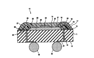
Figure 1 is a cross-sectional side view of an
exemplary integrated circuit package 10 in accordance
with the present invention. Substrate 11 forms an
insulating base of package.l0. Substrate 11 has an
upper first surface 12 and a lower second surface 13.
Substrate 11 may be formed, for example, of a
conventional epoxy laminate or ceramic. Examples of
suitable substrates include Mitsubishi BT, Arlon 45N,
and Nelco BT laminate substrates.
An exemplary thickness of substrate 11, between
~~irst surface I2 and second surface 13, is between 0.36
mm and 0.56 mm, but the thickness of substrate 11 may
vary depending on the application. The perimeter of
substrate 11 may be a variety of shapes, again
depending on the packaging application. For example,
the perimeter of substrate 11 may be square or
rectangular.
Integrated circuit die 14 rests on and is affixed
to first surface 12 of substrate 11. Die 14 has an
-S-
CA 02301615 2000-02-24
WO 99/13515 PCTNS98/17999
upper first surface 21 containing peripheral bonding
pads 19, peripheral side surfaces 22, and a lower
second surface 23 opposite first surface 21.
Conventional epoxy die attach compound, such as QMI 696
available from the QMI Company of San Diegp, _.-
California, may be used to affix lower second surface
23 of die 14 to first surface 12 of substrate 11.
Typically, EPROM, CCD or other optical integrated
circuit dies have vision cells or other light-sensitive
circuitry on their upper surfaces, which must be
selectively or continuously exposed to light of a
selected frequency for some functioning of the
completed device. In Figure 1, such circuitry is
exemplified by polyimide vision cell 24 on a central
portion of upper first surface 21 of die 14. Other
non-optical circuitry, not shown in Figure 1, may also
be exposed on first surface 21 of die 14, depending on
the application.
Conductive metallized via 15 extends through
substrate 11, between first surface 12 and second
surface 13. Via 15 may be formed, for example, by
drilling a hole through substrate 11, and plating the
hole with metal, such as copper, using conventional
methods. Via 15 provides a conductive path for
electrically connecting conductive structures on first
surface 12 and second surface 11 of substrate 11.
In Figure 1, conductive structures on or adjacent
to first surface 12 of substrate 11 electrically
connect die 14 to metallized via 15. For example, at
the intersection of via 15 and first surface 12 of
-6-
CA 02301615 2000-02-24
WO 99/13515 PCT/US98117999
substrate 11., a first end of a metal trace 16 is
electrically connected to via 15. Metal trace 16
extends laterally away from via 15, and its second end
is electrically connected to a metal contact 17 on
first surface 12 of substrate 11. The term __
"electrically connected" is used broadly herein to mean
a conductive path exists between the "electrically
connected" structures, which may be due to a direct or
indirect physical connection.
Contact 17 is electrically connected to a first
end of a metal bond wire 18. An opposite second end of
bond wire 18 is electrically connected to a conductive
bonding pad 19 on a peripheral portion of upper first
surface 21 of die 14.
Metal trace 16 and metal contact 17 may be formed,
for example, of copper that is plated on first surface
12 of substrate 11 using conventional electroplating
methods. Bond wire 18 may be formed of gold or
aluminum.
A typical package like Figure 1 will have multiple
metallized vial 15, metal traces 16, contacts 17, bond
wires 18, and bonding pads 19, the number of which
would depend on the application. For clarity, only two
of each of these structures are shown in Figure 1.
Metallized via 15 also intersects lower second
surface 13 of substrate 11. At second surface 13, a
first end of metal trace 31 is electrically connected
to metallized via 15. Metal trace 31 extends laterally
on lower second surface 13 away from via 15. A second
end of metal trace 31 is electrically connected to a
_7_
CA 02301615 2000-02-24
WO 99113515 PCT/US98/17999
planar metal interconnection ball land (not shown),
which is also formed on lower second surface 13 of
substrate ~il. A metallic solder interconnection ball
33 is joined to the land. Interconnection balls 33 are
used to electrically connect package 10, and hence die ---
14, to external circuitry such as a circuit board. In
alternative embodiments, an interconnection ball land
may be formed on the lower second surface of the
substrate around the metallized via, as opposed to a
lateral distance from the wia, so that an
interconnection ball may be placed directly below the
via.
A typical package like Figure 1 would have
multiple metal traces 31, metal lands, and
interconnection balls 33 on the lower second surface 13
of its substrate 11, the number of which would depend
on the packaging application. For clarity, only two of
these structures are shown in Figure 1.
The interconnection balls 33 of Figure 1 are
characteristic of a ball grid array ("BGA") package.
Such interconnection balls are generally arranged in an
'array pattern , such as X and Y axis rows of balls, on
second surface 13 of substrate 11. The particular
pattern selected may depend, for example, on the
external circuitry to which package 10 is ultimately
electrically connected.
The interconnections of the various conductive
structures described above, including metallized vias
15, metal traces 16 and 31, contacts 17, bond wires 18,
metal lands, and interconnection balls 33, provide an
_g_
CA 02301615 2000-02-24
WO 99/13515 PCT/US98/17999
electrically conductive path between bonding pads 19 of
die 14 and interconnection balls 33. Metallized vias
i5 provide the portion of the conductive path that
extends through substrate 11.
There are, of course, other ways knov~n to --'
practitioners to electrically connect an integrated
circuit die (or dies) in a package to conductive
structures on the exterior of the package or to connect
the package itself to external circuitry. As an
example, instead of using solder interconnection balls
33, a patterned array of planar metal contacts may be
formed on lower second surface 13 of substrate 11, as
in a conventional leadless chip carrier ("LCC")
package. As another alternative, instead of using bond
wires, tape automated bonding may be employed.
Returning to Figure 1, bead 20 is adjacent to and
covers the peripheral edges of die 14 on first surface
12 of substrate 11. Bead 20 has a top first portion
25, an opposite lower second portion 26, a outer third
portion 27, and an inner fourth portion 28 adjacent to
die 14. Top first portion 25 of bead 20 forms a
peripheral portion of the top surface of package 10.
Lower second portion 26 of bead 20 is on and fixed to
first surface 12 of substrate 11. Outer third portion
27 of bead 20 forms the peripheral side walls of
package 10. Inner fourth portion 28 of bead 20 covers
side surfaces 22 of die 14, as well as the outer
periphery of upper first surface 21 of die 14,
including the interconnections between bond wires 18
and bonding pads 19 on die 14.
_g_
CA 02301615 2000-02-24
WO 99113515 PCT/US98117999
As shown in Figure 1, bead 20 protectively covers
each metal trace 16, contact 17, bond wire 18, and
bonding pad 19 located on or adjacent to first surface
12 of substrate 11. Bead 20 also covers side surfaces
22 of die 1'4 and the periphery of upper first- surface --'
21 of die 14, including bonding pads 19. Head 20 does
not, however, cover the central portion of upper first
surface 21 of die 14 where polyimide vision cell 24 is
located, to avoid interference with the light-sensitive
functioning of vision cell 24. The height of bead 24
above first surface 12 of substrate 11 exceeds the
height of die 14 and bond wires 18 above first surface
12. Accordingly, bead 20 and upper first surface 21 of
die 14 together form and define a cavity, above die 14,
into which a thin layer of transparent encapsulating
material 29 is deposited.
Figure 2 is a top view of an incomplete package
10, before a transparent encapsulant is placed onto die
14. In Figure 2, bead 20 surrounds die 14, contacting
side surfaces 22 of die 14 all the way around die 14.
To illustrate that bead 20 also covers the periphery of
upper first surface 21 of die 14, the periphery of
first surface 21 of die 14 is shown by dashed lines.
Although die 14 and bead 20 are shown as having square
perimeters in Figure 2, the perimeters of die 14 and
bead 20 may vary depending on the application. For
example, die 14 and bead 20 may have rectangular
perimeters.
Bead 20 is formed of a material that is adhesive.
The material of bead 20 should also be somewhat viscous
-10-
CA 02301615 2000-02-24
WO 99/13515 PCT/US98I17999
and flowable.when initially applied onto first surface
12 of substrate 11, but should be readily hardenable by
air drying or heating or the like so that bead 20 forms
solid,-protective side and .top surfaces of package 10.
' An exartiple material useful for bead 20 is epoxy, __ -
such as Ciba Nagase 9006 epoxy from the Ciba Nagase
Company of Japan. Hardening of this epoxy is normally
accomplished by heating for about 60 minutes at 150°C.
Other suitable epoxy materials usable for bead 20
include Hysol 4451 from Hysol Corporation of City of
Industry, California. Alternatively, instead of epoxy
material, bead 20 may be formed of a silicone rubber,
such as silicon rubber number 3140 from the Dow Corning
Company.
In Figure 1, a planar layer of transparent
encapsulant 29 covers first surface.21 of die 14,
including the central portion of first surface 21 of
die 14 where polyimide vision cell 24 is located. When
hardened, encapsulant 29 forms a top exterior surface
of package 10.
Encapsulant 29 is contained within the square-
sided cavity above die 14 which was formed by first
surface 21 of die 14 and that part of inner fourth
portion 28 of bead 20 whose height above first surface
12 of substrate 11 is greater than the height of die 14
above first surface 12 of substrate 11.
In Figure 1, the exemplary planar upper first
surface 30 of encapsulant 29 is slightly lower, for
example, about 0.005 mm lower, than top first portion
-11-
*rB
CA 02301615 2000-02-24
WO 99113515 PCT/US98/17999
25 of bead 20, which may provide protection from
abrasions to first surface 30.
The appropriate thickness of the layer of
encapsulant 29 depends, for example, on the packaging
application'and the material chosen for encapsulant 29:.__-
A typical material appropriate for encapsu~ant 29 has a
light transmission value that is a function of'its
thickness.
Encapsulant 29 is formed of a material that is
adhesive. The material of encapsulant 29 should be
somewhat viscous and flowable when initially applied
onto first surface 21 of die 14, but should be
hardenable so that the layer of encapsulant 29 forms a
solid, protective top surface of package 10 adjacent to
die 14.
As discussed above, the EPROM, CCD, and other
optical sensing device applications suited for a
package such as Figure 1 require that a surface of the
packaged die be selectively or continuously exposed to
light of a selected frequency. In such applications,
the material chosen for encapsulant 29 should be
'transparent to the particular frequency of light needed
by the application.
In the example of Figure 1, die 14 has a polyimide
vision cell 24 located on a central portion of first
surface 21 of die 14. As is typical in CCD or other
optical sensing applications, such a vision cell
requires exposure to visible light. For such
applications, as shown in Figure 1, encapsulant 29 is
formed of a clear material, such as clear TEFLON~
-12-
CA 02301615 2000-02-24
WO 99113515 PCTIUS98/17999
synthetic polymeric resin (polytetrafluoroethylene)
from the E. I.. Dupont Chemical. Company, or an
equivalent transparent, protective material. A layer
of TEFLON~ resin~having a thickness of about 0.20 mm
may be hardened by heating at a temperature o~ about. -.-
150°C for about 60 minutes. Alternatively, a layer of
water white clear epoxy may be used for encapsulant 29.
The dimensions of a package like Figure 1 will
vary with the particular packaging application. As an
example, dimensions of components of package 10 may
include an approximately 10 mm x 10 mm square substrate
11; an approximate 8 mm by 8 mm square die 14; a bead
having an approximate 9 mm x 9 mm square perimeter;
a bead 20 height between top first portion 25 and first
15 surface 12 of substrate ll ranging from approximately
0.60 mm to 0.80 mm; a bead 20 width between outer third
portion 27 and side surfaces 22 of die 14 ranging from
approximately 0.60 mm to 0.80 mm; and a relatively thin
layer of a transparent encapsulant 29 having a
20 thickness, i.e., a height between upper first surface
21 of die 14 and upper first surface 30 of encapsulant
'29, ranging from approximately O.lO mm to'0.30 mm. As
an example, the thickness of encapsulant 29 may be 0.20
mm. Again, such dimensions will vary with the
packaging application. For example, larger dies
typically require larger packages.
Figure 3 shows a flow chart for an example method
of making a package in accordance with the present
invention. As a first step A in the process shown in
Figure 3, an insulating substrate base is provided
-13-
CA 02301615 2000-02-24
WO 99/13515 PCTIUS98/17999
having conductive structures on and between its first
and.second surfaces. As an example, substrate 11 of
Figure 1 i-s provided. In Figure 1, substrate 11 has
metal traces 16 and 31, metallized vias 15, contacts
17, metal lands, and interconnection balls_ 33, all of _.
which are electrically connected.
As a second step B, an integrated circuit die is
provided and placed on the first surface of the
substrate. A conventional epoxy die attach material
may be used to affix the die to the substrate.
As a third step C, the integrated circuit die is
electrically connected to the conductive structures on
and through the substrate. Using the example of Figure
1, bond wires 18 are connected between bonding pads 19
on the periphery of die 14 and contacts 17 on substrate
11 so that die 15 may be electrically-connected to
metallized vial 15, and hence to interconnection balls
33. A conventional bond wire attaching machine may be
used to perform this step.
A fourth step D is the application of a bead of a
viscous, hardenable, adhesive material onto the first
surface of the substrate, around the integrated circuit
die. The bead should be applied so that its height
relative to the upper first surface of the substrate
exceeds the height of the die above the substrate. In
this way, a cavity is formed above the upper first
surface of the die into which the transparent
encapsulant material may be deposited. Figures 1 and 2
show an exemplary bead 20. In those figures, the bead
was applied anto the substrate so as to cover the side
-14-
CA 02301615 2000-02-24
WO 99113515 PCTlUS98/17999
surfaces of the die and the periphery of the upper
first surface of die, as well as the bond wires and
other conductive structures on the first surface of the
substrate. The bead material does not cover the die's
light-activated circuitry: - --
An example bead material is epoxy, such as Ciba
Nagase 9006. Such an epoxy bead may be applied using a
syringe. Alternatively, a conventional autodispense
machine, such as model 5000 of the Camelot Company or
the Millennium model of the Asymtek Company,. may be
used.
A fifth step E is to harden the bead material.
The hardened bead material forms solid, protective side
and top surfaces of the package. Figure 1 shows an
example of a solid bead 20. Where epoxy material is
used for the bead, the step of hardening the bead
material may be performed by heating to a temperature
of approximately 150°C for about 60 minutes.
After the hardening step, a sixth step F is to
apply a layer of a viscous, hardenable, adhesive, and
selectively-transparent encapsulating material onto the
exposed upper first surface of the die, within the
three-dimensional cavity formed by the upper first
surface of the die and the now-hardened bead material
that surrounds the die. Figure 1 shows how an
embodiment of a package appears after a layer of
transparent encapsulant 29 is deposited onto upper
first surface 21 of die 14.
-15-
CA 02301615 2000-02-24
WO 99/13515 PCT/US98/17999
Where, for example, the package is for CCD
applications or other optical applications, the
encapsulating material should be clear so as to be
transparent to visible light. An example material is
clear TEFLON~ resin. - w
The step of applying a layer of a selectively
transparent encapsulating material onto the die may be
performed, for example, with a syringe or a
conventional autodispense machine. The amount of
encapsulating material used affects the thickness of
the layer.
A seventh step G is to harden the layer of
encapsulating material applied onto the die. This
hardening step is performed so that the encapsulating
material forms a solid and protective top exterior
surface of the package. This hardening step may be
performed, for example, by heating the package after
the encapsulating material is applied.
Depending on the package configuration, as an
additional eighth step H, conductive structures such as
solder interconnection balls are placed by conventional
methods onto metallizations provided on the underside
of the substrate of the package. For example, Figure 1
shows a package 10 having solder interconnection balls
33 on second surface 13 of substrate 21.
Alternatively, such conductive structures could be
initially provided on the substrate.
In an alternative method, instead of constructing
each package individually, an array of packages similar
to those of Figures 1-2 are created on a single,
-16-
CA 02301615 2000-02-24
WO 99/13515 PCT/US98I17999
relatively larger substrate, and then the array is cut
apart to separate the individual packages from each
other.
Figure 4 is~a top view of an array 40 of four
incomplete packages 10, before the step of_apply,ing --'
bead material is performed. While array 4~0 shows only
four incomplete packages, the number of packages in the
array can vary, depending, for example, on the size of
the substrate and dies.
In this alternate method, the first three steps
A-C of Figure 3 are performed, i.e. providing an
insulating substrate having conductive structures,
providing and affixing an integrated circuit die to the
substrate, and electrically connecting the die to the
conductive structures on the substrate, except that a
larger substrate 41 having four sites for placement of
integrated circuit dies is provided, and the other
steps are repeated to accommodate each of the four
integrated circuit die that are affixed to substrate
41.
A fourth step is to apply a square bead, like bead
20 in Figures 1 and 2, peripherally around each die on
array 40 of Figure 4. In an alternative embodiment,
the step of applying a bead of adhesive material is
performed by applying a first set of parallel beads of
adhesive material adjacent to the integrated circuit
dies, and then applying a second set of parallel beads
of adhesive material perpendicularly across the first
set of parallel beads, so that a crisscrossing pattern
of rows and columns of bead material is deposited on
-17-
CA 02301615 2000-02-24
WO 99/13515
PCT/US98117999
the substrate around all sides of each die. The
crisscrossing beads meld to form a continuous bead
around each die in the array. As discussed above, the
bead' and the upper first surface of the die together
define a cavity above the die, into which the- layer. of
encapsulating material is deposited.
Referring to Figure 4, after the step of applying
bead material onto substrate 41 is performed, the fifth
through eighth steps E-H of Figure 3 are performed for
i0 each package in the array, i.e. the steps of hardening
the beads, applying the layers of encapsulant within
the cavities formed by the beads, hardening the layers
of encapsulant, and placing conductive structures such
as interconnection balls on the second surface of the
substrate for each site on the array.
Subsequently, a step of separating the individual
packages in the array of packages from each other is
performed. This step may be performed, for.example, by
cutting through the substrate and bead material using a
conventional wafer saw.
The embodiments of packages and assembly methods
described above are merely examples of the present
invention. Artisans will appreciate that variations
are possible within the scope of the claims set forth
below.
-18-