Note: Descriptions are shown in the official language in which they were submitted.
-- ;-28, FFB, 2000-18:47 MARKS AND CLERK N0, 0534 P, 6
WO 99110976 PCTIGB98l02583
~omm nications An aratus
This invention relates general)v to the held of radio frequency receivers and
transmitters
(which, when incorporated together in one unit are commonly referred to as
'transceivers). The invention has particular application where such systems
arc
connected to personal computing devices (PCDs), such as laptop PCs or personal
digital
assistants (PDAs).
The use of radio frequency (RF) electromagnetic waves as a carrier for
information, such
as analogue audio, digital audio and general digital data. is welt known in
the
communication art, The mast familiar exploitation of this is found in
tclcvision and
radio, and a typical receiver for FM radio is shown (in block diagram form) in
FIG. 2. In
such a receiver, an antenna 301 converts radio frequency electromagnetic
radiation (RF)
into electrical signals, Since the antenna will convert (to some degree) any
RF, sorne
means is needed to select only the desired signal. which. in the case of
conventional FM
audio broadcasting, will be a particular band of signals with a particular
centre frequency
and a 200kHz bandwidth. This process is known as tuning, and the degree to
which a
receiver is able to acquire only the desired signal and reject all others is
i'nown as its
selectivity. The RF amplifier 302 provides some decree of tuning selectivity,
commonly
through the use of resonant (LC) circuits on its input and output, The
resonant frequency
of these circuits is set by the tuning control 211, which will commonly
involve variable
capacitors. The RF amplifier Z02 also increases the system's sensitivity
{i,e., its ability to
acquire weak RF signals), by increasing the amplitude of the signal.
To provide a well controlled receiver bandwidth and to reduce the frequency of
the
acquired RF signal, the signal is next passed into a mixer 203, where it is
combined with
a signal from a local oscillator (LO) 210. The frequency of oscillator 210 is
set by the
CA 02301748 2000-02-28
28. FEB. 2000 18:48 MARKS AND CLERK N0, 0534 P. 7
a
WO 99IL0996 _ PCT/G898/OZ583
tuain~ control of the device 211 (and modified by feedback from the automatic
frequency control (AFC) system 209). The result of such RFILO mixing, commonly
referred to as heterodyning, is to produce the sum and difference of the LO
and RF
frequencies (together with a number of other frequencies). If these
frequencies are
denoted fo and fr respectively, then the primary output of mixer ?03 will be
Ifr i fob. In
high sidc injection, which is most usual in such receivers, the fo signal is
higher in
frequency than the desired frequency fr. The difference between them is set to
be the
intermediate frequency, or IF, by the tuning control 211. If we denote this
frequency f;,
then:
fo - fr 1. f~
The purpose of this arrangement is to down-concert the inbound RI~ signal f,
to a fixed
frequency (for that receiver) f" which is then selected by the tuned 1F
amplifier 204,
Because the frequency f, is fixed, the bandwidth of the receiver can be
accurately
controlled, and the IF amplifier therefore provides good selectivity of the fr
- fa IF signal.
Systems such as that illustrated in FIG. 3 are commonly referred to as
superheterodyne
(or superhct) receivers The terms are contractions of "supersonic heterodyne'
because
they Ee~nerate a beat signal at frequencies above human hearing.
Care has to be taken with such an arrangement, however, to prevent the
receiver from
picking up another. unwanted signal, known as the image frequency. This occurs
because
the 5vstem accepts the signal fm = fr -~ 2 f" on which it will operate to
produce (inter
trlia):
f~ ~ fo = (fr'+ 2 f~) - (fr 1' fi) ' f,.
in simple systems such as that illustrated in FIG. 2, good image rejection is
normally
achieved by the tuned 1tF amplifier ?02 suppressing f"",
The I)< signal (which is normally set to f; = 10.7M~z for converaional FM
audio
receivers) is then passed into a peak clipper 205, which simply conditions the
signal (by
CA 02301748 2000-02-28
, 28. FHB. 2000 18:48 MARKS AND CLERK N0, 0534 P, 8
WO 99/i0976 - PCT/G1s98~02583
eliminating amplitude chances due to noise) prior to the action of the
detector 213. The
detector or demodulator, for frequency modulation (FM) convetu changes in the
frequency of the carrier Wave f~ (now represented by in downconverted IF form
as f;) to
changes in amplitude of the original, modulating wave fm. The primary resuh of
stage
? 12, therefore, is she recovered audio information. which is passed to an
audio frequency
amplifier 207 and then on to a reproducer, in this case a speaker ?08 which
renders the
recovered audio information in audible form. Two other supplementary systems
are
linked to the detector. One, the automatic frequency control (AFC) 209, is fed
back to the
oscillator to prevent fo from drifting. Another, the de-emphasis network 306
modifies the
received signal to compensate for the pre-emphasis (treble boost) used in FM
transmission. by reducing the strength of the higher-frequency components of
the audio
sienal
In all of the above discussion. it should be noted that although the RF
carrier centre
frequency and the local oscillator frequency fo are sinele frequency Signals,
the frequency
of the modulating wave fm and the resulting transmitted wave f, will generally
wary over
time (with changes in the amplitude envelope of fm altering the carrier
frequency, for
FM). The difference between the maximum and minimum frequencies of the
modulating
sisnal fm is known as the modulation bandwidth.
In general. modulation operates by shifting one or more of the frequency,
phase or
amplitude of a carrier wave (or set of such carriers) in accordance wish the
modulating
signal's instantaneous amplitude. This process creates sidebands around the
central
carrier frequency, and the difference between the highest frequency
significant sideband
and the lowest frequency significant sideband is known as the transmission
bandwidth.
The complementary process to modulation, which takes place at the receiver
side to
recover the modulating signal is known as demodulation.
A large number of modulation schemes may be used to transmit information via
RF
emissions, and those well known in the art include frequency modulation (FM),
various
CA 02301748 2000-02-28
28. FEB. 2000 18.48 MARKS AND CLERK N0, 0534 P. 9
pCT/G898/0=583
WO 99/10976 _
4
forms of amplitude modulation (tL'~t) (such as full carrier double sideband,
suppressed
carrier double sideband. and suppresstd carrier single sideband), and phase
modulation
(PM); and these techniques may be applied jointly (as with quadrature
amplitude
modulation or QAM, which combines amplitude and phase modulation), and in
parallel
across a number of carriers (as, for example, with the coded orthogonal
frequency
division multiplex (COFDM) used in the Digital Audio Broadcasting system.
defined in
ETS 300 401 rev. 2). The situation is further complicated by the emergence of
spread
spectrum techniques, such as code division multiple access (CDMA), which uses
a wide
transmission bandwidth that is shared by various transmitting stations. each
of which
makes use of a unique code sequence to allow the signal to be distinguished
from that of
the other stations.
Fixed demodulation receivers, such as that shown in FIG. '', are capable of
only a single
demodulation scheme.'.~Sore advanced receivers can demodulate according to a
number
of schemes, For example, a household radio will normally be capable of
demodulating
conventional FM and A1~I, and will also be able to operate across a number of
different
frequency bands. Yet more sophisticated communications receivers, often
referred to as
'scanners', generally implement a laree number of demodulation schcmes, and
can
acquire signals over a very wid-a range of ItF frequencies. However, even
sophisticated
scanners are limited, in that they cannot easily be adapted to demodulate
signals using
modulation schemes that are introduced after they are manufactured.
FIG. 4 shows an overview of a system proposed by Rosecta Labs in WO 9627949,
in
which a pcrsonal computing device (PCD) 405 is connected to a communications
receiver 401 via an interface 402. The PCD 405 displays a man-machine
interface (MMI)
403 through which the user can select the tuning and demodulation options for
the
receiver 401, said information being transmitted to the receiver through the
interface 402,
The PCD 405 can receive demodulated digital information from the device and
then
display the information using the MMI. It can also receive general tuning
information,
and signal summary information, such as an indication of the received signal
strength
CA 02301748 2000-02-28
vv. ...L, ~vvu tu.~v nitlnnJ 111rL u~L.,..
WO 99/t097b - PCT/GB98/oZ583
(RSSI). Note, however, that with this system the PCI7 is only acting as a
sophisticated
tuning controller and reproducer - the demodulation is still performed in a
dedicated
hardware receiver 401.
FIG. 5 illustrates the mechanisms used in the transmission and reception of
intelligence
by liF, as known in the communication aru. ~.t the transmission side 501. an
originating
application 503 generates digital data 504, which is then transformed through
a number
of di~tital protocols 532. These protocols may serve a number of different
functions. and
are commonly arranged in a protocol stack. which maw be analysed aecordine to
the
middle layers (3 through 6) of the Open Systems Interconnect model proposed by
the
International Standards Oreanisation (ISO/OSI):
7 - Application Layer
Connection to PCD applications
6 - Presentation Laver
Formatting transforms for data (file conversions,
etc. )
- Session Layer
Persistent connection management
4 - Transport layer
Safe end-to-end communication
3 - Network Layer
Addressing. routing and switching across a
network
2 - Link Layer
Link-based error detection and correction
1 - Physical Layer
How bits are sent and received
CA 02301748 2000-02-28
28, F,EB, 2000 18:49 MARKS AND CLERK N0, 0534 P. 11
WO 99/10976 _ PCT/G~98/OZ583
6
For example, session control (layer S) could occur here. as could forward
error control,
such as convolutional encoding and the addition of checksums (layer 3).
However, the
important thing in the present case is that the result of the high level data
protocols 532 is
digital data 5051506. ready for transmission.
The next stage is to pass the data into a modulator, in order to encode it
onto a signal
suitable for tranmission at RF. This can be done in a number of ways. The
first,
commonly used by systems which must send data over an existing analogue
transmission
system originally intended for audio (such as a voice-based telecommunication
system),
provides an audio frequency (AF) modulator 508 which renders the data into AF
523,
which is then passed on to a subsequent. higher frequency modulation stage ~
10, in much
the same way as AF 507 coming from a convemional audio source (such as a
microphone
509) would be. The second (and generally more efficient) way to proceed is to
pass the
data SOS directly to the modulator 510_ and then use an appropriate scheme
(such as
QAM) to encode it.
The information can be encoded either directly to RF signal 5l3 by the
modulator 510, or
encoded by the modulator s 10 to IF signal 511, which may then be up-converted
(by 513
which will commonly involve a single or multiple superhet) to RF signal 514,
In any
case. after the modulator stage 510 the information is generally embodied in
analogue
form,
The RI= signal 512/514 is conveyed into the RF transmission subsystem 515
which
provides the necessary buffering, matched emission antenna and so on, The
information
is then propagated through space as electromagnetic waves 516,
These waves may be acquired by a remote receiver station 502, using an
appropriate RF
front end 517 (reception antenna, RF amplifier etc.). The result is electrical
R.F signals
518/530, which, depending on the receiver, may either be directly passed 5?0
to the
demodulator X33, or passed 518 to a down-converter stage S 19 (which will
commonly
CA 02301748 2000-02-28
28. F,EB. 2000 18;49 MARKS AND CLERK N0, 0534 P. 12
WO 99110976 - PCTIGB9BIO2583
7
involve a single or multiple superhet), in which it is shifted to an
intermediate frequency
(IF) 521 and then passed to demodulator >33.
In any event, the (generally analogue) RF 520 or IF 5? 1 signal enters the
demodulator
533, where it is detected. In the case of analoeue audio intelligence, the
detected AF
Signal SZ8 may (after amplification) be passed to a reproducer 53~ (such as a
speaker)
which allows the original audio to be heard. In the case of digital data
encoded within an
AF signal, the recovered intelligence 52~ is passed to an AF demodulator 525,
which is
used to recover the love-level data stream 537. For directly encoded data. the
demodulator
X33 produces the data stream 526. In either case. the data is then passed
526/5?7 to
higher-level, digital data protocols 5?9, which perform operations
corresponding to the
middle layers of the 1501051 model. The resuhing data 530 is then passed to
end-user
applications ~~ 1.
Turning now to FIG. 3, we can see how, in the prior art. this arrangement for
data
transmission outlined in FIG. ~ has conventionally been implemented. Consider
first the
case of an inbound, or forward channel signal. Generally, an antenna ~Ol is
used to
convert electromagnetic RF emissions into electrical sir~nals at RF frequency,
which are
then amplified and subjected to coarse selection by an RF receiver stave 306
(these two
stages correspond to 517 in FIG. 5), then broueht down to an intermediate
frequency (IF)
by a down-converter stage 307 (commonly implemented as a sinele or multiple
superhet,
corresponding to 519 in FIG. 5) before being subjected to a detector stage
308. which
provides the primary demodulation to digital information (or AF),
corresponding to 533
in FIG. 5. These three stages 302 are commonly implemented in a single device,
such as
a cellular telephone 320 or communications receiver 319. The resulting decoded
information. corresponding to 5361524 from fIG. 5, is then passed to a higher-
level
system, which in the case of AF provides secondary demodulation {as per 525 in
FIG. 5)
and in both cases provides much of the higher level data protocols (529 in
FIG. 5). This
stage 303 is generally provided by a plug-in hardware card 317 or an external
modem
31 B, and since it deals with digital or AF input the processes it performs do
not directly
CA 02301748 2000-02-28
28. FEH, 2000 18:50 MARKS AND CLERK N0, 0534 P. 13
WO 99/10976 _ PC'f/G898JOZ5B3
8
depend upon the data having been sent over a radio link. The functions of both
302 and
303 are sometimes combined on a single plug-in card 321. The resulting data
stream is
then passed to the personal computing device (PCD) 314 where it is consumed by
applications (this corresponds to 531 in PIG. ~). At this stage 304 the device
in question
is generally a personal computer. such as an IBM-compatible PC 315, a
'persona) digital
assistant' (PDA) 316, or otherwise.
A similar analysis may be made for the generation of an outbound signal (or
back
channel). Applications on the PCD 314 supply information (corresponding to
X03/504 in
FIG. 5), which is then passed to a high-level protocol~'modulation stage ~ 13
in device
30~. responsib;e for mapping the data through the appropriate protocols (as
per ~~2 in
FIG. ~), and possibly transforming it into /iF (this corresponds to 508 in
FIG, 5), As
with input, the transformations in device 303 do not necessarily produce a
signal that is
specific to transmission over a radio link, since the intelligence is either
r1F or a direct
digital representation on exit. (For example, if rendered to AF, a
conventional land-line
telephone system could be used to send the modulated information to a remote
terminal).
The AF or digital signal is then passed into the radio communications device
~0? which
encodes the signal (generally to analogue 1F: in any event corresponding to
the modulator
510 of FIG. S), up-converts ii 310 (generally using a single or multiple
superhet
arrangement. corresponding to S 13 of FIG. S) and then passes it to an RF
amplif er 309
and antenna 305 which emit the final signal (,these two corresponding to 515
in FIG. S).
The mapping to physical devices is the same for transmission xs reception
(other than the
obvious requirement that the device, be it communications receiver 319. all-in-
one radio
modem card X21 or otherwise. have ItF uansmission capabilities in addition to
the
reception mechanisms just mentioned), It is much more common in such prior art
system
to find a transceiver or receiver-only implementation - transmitter-only
implementations
are fairly rare.
CA 02301748 2000-02-28
28, FEB, 2000 18:50 MARKS AND CLERK N0. 0534 P. 14
WO 99/10976 _ PGT/CB98/OZ583
9
1n the prior art, the use of special hardware, such as digital signal
processor integrated
circuits (DSP ICs) or analoeue detectors (such as a ratio detector for Fl~
demodulation)
have wnventionaliy been employed. However. DSPs are expensive to produce.
expensive to customise for a particular application (since few engineers have
experience
of them), and difficult to update in the field to cope with new modulation
schemes.
Analogue detection circuitry. on the other hand, tends to be extremely
inflexible, and
cannot cope with the emerging breed of complex, and primarily digital.
transmission
protocols. For example, the coded orthogonal frequency division multiplex ;
differential
quadrature phase shift keying (COFDM/DQPSKI modulation of the ETSI Digital
wudio
Broadcasting (DAB) specification (standard ETSI 300 401 rev. ?), is quite
beyond the
scope of analogue decoders,
There is a generally acknowledged need to provide inexpensive. flexible access
to high-
bandu~idth RF wireless data services, includin' both forward and back
channels. to users
of PCDs. However, prior art PCD radio modems, such as 3'? 1 in FIG. 3, are
generally
either very expensive, due to the use of DSP ICs. or unable to transceive at
high data
rates (because they make use of simple, analogue systems such as binary
frequency shift
keying ($FSK), and therefore cannot take advantage of modern high-throughput
schemes
such as COFDM/QPSK or COFDMIQAM). In either case. such modems are generally
inflexible - they are designed to handle only ane (or a small number) of
modulation
schemes and RF frequencies. and furthermore, severally do not provide foturard
compatibility - adapting an existing R.F modem to a neW communications
protocol
usually means buying a new modem. or having an troublesome hardware upgrade
perfotTrted on the device,
It is, correspondingly, an object of the current invention to provide an RF
communications apparatus, intended far use with a PCD and a suite of software
running
thereon, which provides an economical communications system that can easily be
adapted to different modulation and demodulation schemes.
CA 02301748 2000-02-28
28. FEB. 2000 18:50 MARKS AND CLERK N0, 0534 P. 15
WO 99/10976 - PCTlGls98/02583
According to a first aspect of the present invention, there is provided
communications
apparatus comprising means for receiving a modulated radio frequency signal.
at least
one means for down-converting a received modulated radio-frequency signal,
means for
digitising a down-converted signal and means far exporting at least a part of
the digitised
modulated signal to a personal computing device.
According to a second aspect of the present invention, there is provided
communications
apparatus comprising means for importing a digital modulated signal from a
personal
computing device, means for converting the digital modulated signal to an
analogue
signal. means for up-converting the attaloeue signal to a radio frequency
signal and
means for transmitting the radio frequency signal.
In a broad sense, the invention is desisrned to exploit the extremely fast
main processor
integrated circuits (ICs) and lar_e memory capacity available within PCDs.
particularly
IHM-PC compatible machines, The processor chips fitted to such systems are
often
capable of outperforming dedicated digital Signal processing (DSP) ICs, and
have pienty
of spare computing capacity (and other resources, such as memory) available
when the
user is performing the tasks for which PCDs are commonly employed, such as
editing a
spreadsheet, writing a letter, browsing files, and suchlike, The cost of the
said main
processor IC is high, but the user has already paid for the device when he or
she bought
the PCD (unlike the case of the DSP, which must be included in the price of a
DSP-
equipped radio modem). In anv case, the extremely large and competitive market
for
PCDs means that the cost per normalised computational operation (NCO) is lower
for the
main processor IC than the dedicated DSP. Furthermore, the ubiquity of such
ICs ensures
the existence of a large number of sofrware engineers who are familiar with
coding for
such architectures, and the presence of advanced development tools to
facilitate their
efforts. This must be compared with the specialised world of DSP programming,
with all
its artendant expenses.
CA 02301748 2000-02-28
28. FEB, 2000 18:50 MARKS AND CLERK N0, 0534 P, 16
WO 99/10976 ~ PCT/GB98102583
The presem invention thus exploits the availability of 'spare' computing
capacity on the
very device to which the user wishes to Connect a radio receiver, transmitter
or
transceiver (in order to gain access to information services and other ~t,F'
broadcasts,
whether analogue or digital). !t is thus beneficial to make use of this
capacity, rather than
to replicate it by embedding an expensive DSP into the transceiver hardware
(or to use a
restricted analogue component system), One Qf the key advantages of the
present
invention is that it provides the ability to do this. incorporating a
communications
receiver. transmitter or transceiver 'front end' to a digital ff data pump,
which is capable
-of communicating with adaptable software drivers in the PCD over a high speed
data bus.
The drivers are responsible for converting the digitised IF to the modulating
data
contained therein. and for svnthesisinsr digital IF representing the modulated
components
of any outgoing transmission. The ability to use PCD-resident software, and
PCD main
processor cycles, to process the IF information (whether inbound or outbound)
is a key
feature of the common invention. It allows the device to be manufactured at a
relatively
low Lost, yet be able to process complex, high-bandwidth RF signals (with a
correspondingly high bit throughput), be capable of handling a wide variety of
modulation protocols, and be easily extendible to cope with new (or modified,
or
previously unaddressed) modulation protocols, with the simple addition of
'plug-in'
software modules on the PCD.
Other optional features of the present invention will be apparent from the
attached
dependent claims.
The present invention will now be described by way of example with reference
to the
accompanying drawings, in which:
FIG. 1 is a functional block diagram showing the major components of one
embodiment
of the radip frequency (RF) adaptor of the present invention. As is the case
with all the
drawings, only the major control and data flows are shown; minor control and
data flows
are not.
CA 02301748 2000-02-28
28, FEB. 2000 18 ; 51 MARKS AND CLERK N0. 0534 P. 17
WO 99/10976 - . PCT/GB98/02583
12
FIG. 2 is a functional block diagram of a frequency modulation (FM1 receiver
for
conventional audio broadcasting, as is known in the prior art.
FIG. 3 is a functional block diagram showing the connection between a radio
frequency
receiver a hardware modern, and a personal computing device (1°CD), as
is known in the
prior art. Examples of systems embodying the various stages are also shown.
FIG. 4 is a functional block diagram of an RF scanning radio controlled by a
PCD, as is
known in the prior art.
FIG. ~ is a conceptual protocol stack diagram, illustrating the end-to-end
process of
content transmission and reception u5ine RF signals,
FIG, 6 is a functional block diagram of the Antenna Control Unit of the RF
adaptor of
the current im~ention (corresponding to 103 in FIG. 1 ), according to a
preferred
embodiment,
FIG. 7 is a functional block diaeram of the radio frequency (RF) reception
amplifier
stage of RF adaptor of the current invention f correspondinst to 10~ in FIG, 1
), according
to a preferred embodiment.
FIG. 8 is a functional block diagram of the down-converter stage of the RF
adaptor of the
current invention (corresponding to 105 in FIG. 1 ), according to a preferred
embodiment.
FIG. 9 is a functional block diagram of the (inbound) anti-aliasing bandpass
filter unit of
the RF adaptor of the current invention (corresponding to 106 in FIG. 1 ),
according to a
preferred embodiment.
CA 02301748 2000-02-28
28. FEH, 2000 18:51 MARKS AND CLERK N0. 0534 P, 18
WO 99/10976 PCT1GB98/02583
FIG. 10 is a functional block diagram of the analogue to dieital converter
(ADC) unit of
the RF adaptor of the current invemion (correspondine to 107 in FIG. 1 ),
according to a
preferred embodiment.
FIG. 11 is a functional block diagram of the interlace management unit (iMU)
of the RF
adaptor of the current invention (correspondine to 108 in FIG. 1 ), according
to a
' preferred embodiment.
FIG, 1 ~ is a functional block diaeram of the digital to analogue converter
(DAC) unit of
the RF adaptor of the current invention (corresponding to 110 in FIG. 1 ),
according to a
preferred embodiment
FIG, 13 is a functional block diagram of the (outbound) anti-aliasing bandpass
filter and
combiner of the RF adaptor of the current invention (corresponding to 111 in
FIG, 1 ),
accordine to a preferred embodiment.
FIG. 14 is a functional block diagram of the up-converter stage of the RF
adaptor of the
current invention (corresponding to 1 !? in FIG. 1 ), accordine to a preferred
embodiment.
FIG. 1 ~ is a functional block diagram of the RF transmission amplifier stage
of the RF
adaptor of the current invention i correspondine to 11 ~ in F1G. 1 ),
according to a
preferred embodiment,
FIG. 16 is an exploded diagram showing an embodiment of the RF adaptor of the
current
invention fitted as an internal card (such as a PCI card) within a personal
computing
device (PCD).
FIG. 17 is a tear view of a personal computing device (PCD), showing how two
differem
embodiments of the RF adaptor of the current invention may be connected; one
via a
CA 02301748 2000-02-28
-28. FIB. 2000 18 : 51 MARKS AND CLERK N0. 0534 P. 19
WO 99110976 - 1PCT/G>g98/02583
1-~
high-speed parallel bus (such as the SCSI bus) and the other via a high speed
serial link
(such as the USB).
FIG. 18 is a three-quarter view of a portable personal computing device (PCh),
showing
how an embodiment of the R.F adaptor of the current invention, in the form
factor of a
PCbiCIA card, may be fitted to said 1?CD.
FIG. 19 is a functional block diagram of the software driver structure which
exists on the
personal computing device (PCT7) to which the RF adaptor of the current
invention is
fitted according to a preferred embodiment.
FIG. 30 is a functional block diagram showing the major components of one
embodiment
of a simple radio frequency (RF) receiver adaptor of the present invention.
FIG. ? 1 is a flowchart showing how a simple demodulation process (in this
case. of a
signal modulated using binary frequency shift keying) may be performed by
driver
soft<vare running on the personal computing device (PCb) to which the RF
adapter of the
current invention is fitted, according to a preferred embodiment. Only the
physical layer
of the IS0/05I model is shown,
FIG. ?2 is a flowchan showing how a simple modulation process (in this case,
using
binary frequency shift keying) may be performed by drier software running on
the
personal computing device (PCD) to which the RF adapter of the current
invention is
fitted, according to a preferred embodiment. Only the physical layer of the
ISO/OSI
model is shown.
In the following text, a detailed description will be given of the various
component parts
of the preferred embodiment of the RF adaptor of the current invention.
CA 02301748 2000-02-28
28, FEB. 2000 18;52 MARKS AND CLERK N0. 0534 P. 20
WO 99/10976 PCTIGB98/02583
1?
A very simple. fixed centre frequency, receiver-only embodiment of the RF
adaptor of
the current invention is shown in Fig. 30. An antenna ?012 acquires RF
transmissions
and feeds them into the device ?001 as electrical signals 2007. There, the
signals are
amplified and subjected to a deeree of frequency selection by an RF amplifier
200?. The
resulting amplified RF signal 2008 is then passed to a down-converter 2003,
which, using
a fixed frequency local oscillator superhet arrangement, selects the
appropriate bandwidth
signal and shifts it down in nominal centre frequency to a low intermediate
frequency
(IF) signal. This IF signal 2009 is then passed into an analogue to digital
converter unit
2004 where it is passed throush an anti-aliasing filter and then digitised.
The resulting
digital data stream 2010 is passed to an interface management unit (IMU) 2005,
which
controls access to a high speed bus 2011, through which the (still modulated)
digitised IF
signal is passed into the persona) computing device (PCD) 2006. As the data is
received
into the PCD 2006 ii is processed by software modules contained therein to
provide
demodulation and higher level data processing. The demodulated data is then
either
stored or presented to a user,
The overall scheme of operation for a more complex system, capable of both
transmission and reception, and able to operate over a number of different
nominal centre
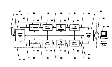
frequencies and bandwidths. may best be appreciated with reference to FIG, 1
(a high-
level block diagram showing the major components of one embodiment of the RF
adaptor device 102 of the current invention). In the system,-RF signals are
acquired by
the antenna 101, and passed 11 ~ into an antenna conrrol unit 103, which
provides various
matching, switching and diversity functions. and provides LF traps to protect
against IF
breakthrough. The resultant RF signal 116 is then passed into an 1ZF amplifier
104, which
provides a degree of selectivity (variable, tuned response) and sensitivity
(by boosting the
RF signal strength). The amplified RF signal is not amenable to direct digital
processing
however, since it will often be at 100s of MHz, which is well above the
ability of current
PCD processor ICs and data transfer busses, not to mention analogue to digital
converters
(ADCs). Since the bandwidth of the signal is what is important, however, and
not the
nominal centre frequency at which it is transmitted, the RF sienal 117 is next
passed into
CA 02301748 2000-02-28
28, FER. 2000 18:52 MARKS AND CLERK N0, 0534 P. 21
WO 99/10976 PCIYGB98/02583
16
a down-converter 10~, which translates the desired frequency band to an
appropriate
intermediate frequency (IF) The down-converter also provides additional
selectivity and
amplification of the desired sienal,
The 1F signal 118 is then passed into a bandpass filter system 106, the
primary purpose of
which is to restrict the higher frequency components of the signal, to prevent
aliasing of
the signal captured by the analogue to digital converter (ADC) 107, into which
the
filtered IF signal 119 is next passed. The purpose of the high speed. high
precision ADC
_. , unit I07 is to render a digital. sampled version of the IF waveform,
which is then
amenable to further disital processing. The digitised data stream is passed
(on a
continuous basis) across data bus 1?0 to the interface management unit (IMLI)
108. The
purpose of the IMU is to manaee all system functions within the device, and to
control
the flow of data between the device 103 and the PCD I09. Inbound. the
digitised IF
signal is buffered within the 1\1L; and transferred to the PCD 109 as
appropriate, using a
fast bus 1 1-I.
The inbound. dieitised IF si~tnal is then processed by software modules within
the PCD
109, making use of the aforementioned spare capacity (as and when available)
on the
PCD's main processor IC (or ICs). These modules demodulate and decode the IF
signal.
and provide any higher level protocol handling (including secondary, AF
demodulation if
needed) that may be necessary. Data thus recovered may be used by applications
running
on the PCD, or passed along to other systems as desired:
When data is to be transmitted from the PCD 109 by the device 10?, the
software
modules running on the PCD I09 must first perform any necessary encoding and
modulation (including high level data protocols, and initial AF modulation if
desired),
thereby yielding a synthesised digital ff signal. This information is passed
via the high
speed bus 1 I~ to the IMU 108, where it may be buffered before being streamed
12I to a
high speed, high precision digital to analogue convener (DAC) unit 110. This
converts
the digital IF signal into an analogue representation 132, which must then be
sent through
CA 02301748 2000-02-28
28. FEB. 2000 18;52 MARKS AND CLERK N0. 0534 P. 22
w0 99/10976 PCT/GH98/o2583
17
an anti-aliasing filter 111, the primary purpose of which is to remove
unwanted high
frequency components which are a natural bv-product of the digital to analogue
Conversion process. The f"~ltered IF signal 123 is then passed into an up-
converter unit
112. which shifts it upwards in nominal centre frequency to the appropriate
range for
transmission (which will. of course, vary depending on the service in use).
The up-
converter also provides sienal amplification and selectivity at the IF range.
The re5uhing up-converted 1ZF signal 1?4 is passed into the (outbound) RF'
power
amplifier 113, which increases its strength to a level appropriate for
transmission. This
amplified signal 1?5 is then passed to the antenna control unit 103, where it
is connected
to the appropriate antenna 101 for transmission. The antenna 101, which may be
shared
with the receiver antenna or distinct from it. then emits the li.F signal as
electromagnetic
waves, and the cycle is complete.
The device is capable of receivins and transmirting information over a wide
number of
nominal centre frequencies and signal bandwidths. Control information
affectinfi the
frequency and bandwidth selectivity of the device is generated by the drivers
on the PCD
109. under ultimate control of a man-machine interface (IVIMI). This
information is
conveyed to the IIVILi 108 over the data bus 11.x, and is then relayed by the
IML' 108 to
the various other component modules of the device 103 over the control bus I
?6. This
bus is also used to transmit performance information (such as signal strenatlt
indications
and tuning feedback) from the modules to the aVIU 108. and between the modules
themselves.
The device is capable of operating in a full duplex mode (simultaneous receive
and
transmit), as well as half duplex (receive and transmit, but never at the same
time) and
simplex (only either receive or transmit, but not both), Outbound
transmissions can have
a completely different modulation scheme. bandwidth and nominal centre
frequency
from the received signals, if desired. The device 102 is also able to 'scan'
through
various bandwidths and frequencies. Alternatively, or in addition, 'scanning'
through
CA 02301748 2000-02-28
28. FEB, 2000 18:52 MARKS AND CLERK N0. 0534 P. 23
WO 99/109'16 FCC/GB9g/02583
18
modulation schemes may take place at the PCD 109 side. to acquire a signal of
interest.
Note that the system can also process digital tuning information contained (as
digital
intelligence) within the inbound signal. to allow it to effect a frequency
(and possibly
modulation) transition to ~ follow' the transmission. which is useful for
channel-hopping
schemes (and for 'handovers' between services, for example bA.B (Digital Audio
Broadcasting) and conventional FM).
As will be appreciated, the device 102, connected to a PCD 109 as per the
above
-description (and as discussed in greater detail in the following text)
provides a unique
low cost, high value RF transceiver system although the receiver and
transmitter may be
provided independently. This system is very flexible. and may be made
compatible with
future modulation standards through changes to the PCD software. It can
operate on
wideband and narrowband transmissions, and can (with the appropriate software
drivers)
receive and transmit single carrier. multiple carrier and spread spectrum
signals,
The various components of the preferred embodiment of the RF adaptor of the
present
invention will now be discussed is more detail,
ANTENNA CONTROL UNIT
The first such component is the antenna control unit. corresponding to 103 in
FIG. 1. and
shown in greater detail irr FIG. 6. This subsystem 601 is fesponsible for
managing the
connection of the various )<tF amplification stages of the transceiver (both
receive and
transmit) to a set of antennae 602. The purpose of any given antenna in the
set 602 is to
convert outbound RF elecuical signals into RF electromagnetic emissions, and
inbound
RF electromagnetic emissions into RF electrical signals. The antenna switch
603 selects
which antenna from the set 602 is to be connected to the iZF outbound signal
path 610
and/or inbound signal path 623. This system allows a single antenna to be
shared for
transmission and reception, either in a half duplex switehover mode, or in a
mixed signal
mode, and also provides the basis of a multiplexed antenna diversity system.
The switch
CA 02301748 2000-02-28
28. FEB. 2000 18:53 MARKS AND CLERK N0, 0534 P. 24
WO 99/109'76 PCT/G~98/02583
19
is (ultimately) controlled by the operating mode selected by the end user and
conveyed to
the PCD system ( 109 in FIG. 1 ) via a ~, this information being translated
into an
antenna switching profile by the driver software (discussed later), which
communicates it
to the interface management unit ( 108 in FIG. 1 ), which in turn issues (ow-
level
commands to the amenna switch 603 through the control bus 608. Within the
antenna
subsystem, a bus management unit 607, co-ordinates the main flow of
information
between subsystem components and the main feed onto and from the command bus
631.
The antenna tuning and matching unit (ATMLi) 604 provides a number of
functions. Its
primary purpose is to couple the selected antenna or antennae ftom the set b02
to the rest
of the system in an efficient manner. In the preferred embodiment, this system
will
include switchable baluns, a variable IF trap'(consisting of a set of parallel
resonant
circuits. or equivalent surface acoustic wave or crystal filters. tuned to the
IF frequencies
injected elsewhere in the receiver, connected between each chosen antenna arid
earth),
and other systems as are well known in the alt to tune a particular antenna to
receive or
transmit within a particular frequency band. It also provides a degree of
transient
isolation between the antenna set 602 and the rest of the system. Control
input is passed
to the ATMU 604 via the command bus 608 and hence through control line 61~,
which
will allow selection of different baluns, IF filter rejection profile, and so
on.
The A~'lvfU 604 is connected to the RF reception and transrttission parts of
the system,
via an inbound 616 and an outbound 617 line. Feeds taken ofFthe 'raw' signals
to and
from the ATMU 618 and 619 ate passed to the antenna performance monitor 605,
which
also receives inputs of the signals 6~3 and 610. The performance monitor is
responsible
for determining metrics of the degree of ' match' that has been attained
between the
chosen antennae set and the signal feeds to and from the rest of the system,
such as the
voltage standing wave ratio (VS1~VR). These metrics are also used to provide
safety
switching, closing off the transmission system when no antenna is available
(because the
user has disconnected it, for example). Information from the antenna
performance
monitor is fed back 615 onto the control bus 608, where it will be used by the
interface
CA 02301748 2000-02-28
28. FEB, 2000 18;53 MARKS AND CLERK N0, 0534 P. 25
WO 99/10976 PCT/GH98lOZ583
management unit (and higher level software in the PCD) to make qualicv of
service and
antenna matching and switching decisions,
Finally within this subsystem. the optional antenna tracking controller 606 is
used for
those antenna which have electronically controlled variable reception
capabilities. For
example, a satellite dish system might have the capability to move the dish
through a
particular sweep, and this functionality would be controlled through the
antenna tracking
controller. As another example. external antenna systems with built-in
amplifiers would
have their gain controlled throuEh this system. In one embodiment, the
tracking
controller is an input/output 1C. with lines 613 that can be programmed.
modified and
interrogated by lti~h-level drivers running on the PCD, via the conuol bus
614, This
arrangement allows the llexibilitv to extend the system to control many types
of antenna
and primary signal acquisition systems.
RF RECEPTION AMPLIFIER
The inbound sisnal 6l6 is passed from the antenna control unit 601 to the RF
reception
amplifier, corresponding to 104 in FIG. 1, and shown in detail in FIG. 7, The
RF
electrical signal 70B into the amplifier subsection 701 is first subjected to
an
electronically controlled bandpass filter, '102, which provides a first
rejection of signals
outside the desired band. This filter may be switched out of circuit entirely
when desired
(for very weak signals). The resulting filtered signal 730 is then subjected
to the
wideband radio frequency amplifier 718. The amplifier may be coned to provide
some
degree of selectivity towards the inbound signal 7?0, and to suppress the
formation of
undesired image, cross-modulation and interznodulation products within the
subsequent
down-conversion stage; generally, this will be provided by a post-
amplification bandpass
filter incorporated within the unit 718. The centre frequency and bandwidth of
the
bandpass filter 702, and the coarse tuning provided by the RF amplifier 718,
are selected
by the rough tuning controller 704, through interface lines 714/713. This
tuning is
ultimately under the control of the MMI on the PCD, which then, through the
appropriate
CA 02301748 2000-02-28
28. FEB. 2000 18:53 MARKS AND CLERK N0. 0534 P. 26
WO 99/10976 PCT/GB98/D25$3
21
software driver modules, sends tuning commands to the IMU, which in turn sends
commands via the control bus 707 to the RF reception amplifier 701 (inter
alia). Within
the amplifier subsystem 701, the bus management unit 706 manages the flow of
information to and from 717 the control bus to components of the subsystem.
including
the aforementioned tuning control (via 715).
The amplifier unit itself 718 consists. in one embodiment. of a set of
switchable
amplifiers, each with a distinct 'fingerprint' of bandwidth, gain, frequency
and phase
response. In such a system. the appropriate amplifier is switched into circuit
by the rough
tuning controller 704, In the preferred embodiment of the system, however, a
single,
relatively wideband amplifier is used. with tuning effected by an inteEral
digitally
controlled bandpass filter unit managed by the rough tuning controller 704
through line
713.
Of course. a primary purpose of the RF amplifier is to provide a degree of
signal gain. Ac
nominal reception frequencies below around 3MHz, the amplifier will be sec to
have very
low gain (or be switched out of circuit altogether), because the overall
signal-to-noise
ratio (SNR) will not be improved by amplification. At higher frequencies, the
noise
picked up by the amenna (relative to the noise generated in the receiver)
falls, making RF
amplification worthwhile from an SNR point of view. Overall level optimisation
to
subsequent subsections of the transceiver, particularly the down-converter. is
achieved by
setting the appropriate gain. This is managed by the prirriarv gain controller
72?, which
has a coarse input set (in the manner now familiar from the preceding
discussion) by the
PCD-resident driver software, communicating via the 1MU and control bus 707
under the
supervision of the bus management system 706, through control line 719. Note,
however,
that the amplifier subsystem 701 also contains a primary gain monitor unit
705, which
accepts pre-filter 712, post-filter 721 and post-amplification 710 signals.
and computes a
continuous signal strength metric for each one. This system feeds its results
706 via the
bus management unit (BMLJ) to the command bus 707, for the ultimate
consumption of
the PCD-resident drivers, but is also capable of operating in a direct
feedback automatic
CA 02301748 2000-02-28
28, FEB, 2000 18;54 MARKS AND CLERK N0. 0534 P, 21
WO 99110976 PCT/GB98/02583
gain control mode. in which the information computed is passed 7I 1 to the
primary gain
controller 722_ to allow rapid equalisation of the sienal, Note that the
amplifier 718
should ex:iibit extremely good linearity.
DOWN-CONVERTER
Having undergone amplification and selection within the RF reception amplifier
701, the
RF signal is next passed 709 to the down-converter Stage, corresponding to 105
in FIG.
1, and shown in detail in FIG. 8. The overall purpose of the down-converter
wage 801 is
to render an amplified version of the desired signal at a much lower nominal
centre
frequency (but with identical bandwidth) to the received signal, The goal is
to bring the
signal down to a frequency where it can sensibly be digitised and fed into the
PCD in the
subsequent stages of the system. Primary signal gain is also possible at the
down-
converter staEe, aided by the fact chat a known nominal centre frequency (at
some point
in the down-conversion chain) may be attained, easing amplifier design
(particularly with
regard to bandwidth / frequency response).
The incoming, amplified RF sisnal 816 is passed through a number of
superhecerodyne
stages 808.. _821 which are responsible for shifting the signal to an
appropriate IF point,
providing filtering tv remove unwanted components, and amplifying the signal
to a
useful level, )Cn the preferred embodimem of the RF transceiver of the current
invention,
there are a total of four primary superhet stages (only two 808/821 are shown
in the
diagram, for clarity), followed by a quadrature superhet 809, although designs
with fewer
or greater number of frequency conversion stages are possible. Each superhet
may be
switched out of circuit if required, under control of the intermediate tuning
controller
807, which receives input from the driver software on the PCD, via the IMU and
the
Command bus 810. As before, a BMU B03 is responsible for managing the
intercommunication 861 between the bus 8I0 and the local modules. It provides
the feed
863 to the intermediate tuning controller. The controller in tum sends
messages to each
of the superhet stages via command lines 826/827/825,
CA 02301748 2000-02-28
28, FEB. 2000 18:54 MARKS AND CLERK N0, 0534 P, 28
WO 99110976 PCT/GB98/OZ5g3
~3
In an alternative embodiment designed for maximum frequency agility, a two-
dimensional matrix of superhet stages is prodded, each of which may be
switched in or
out under the control of drivers running on the PCD. In this arrangement,
specialised first
and second stage superhets are used for the initial conversion of microwave,
L~ and
sub-UHF RF.
In another alternative embodiment. so-called 'direct conversion' of the RF
sirrttal is
employed. Direct conversion involves down-conversion in a mixer using an
injected LO
signal at the nominal centre frequency. This process obviates the image
frequency
problem (and correspondins~ image rejection circuitry), but does introduce a
DC
component into the signal, because the LF is 'wrapped around' the OFiz point.
This DC
component causes serious problems with regard to amplification (see, for
example,
Abidi. A., "Low-Power Radio Frequency ICs for Portable Communications", pp. 58-
60,
in Larson, L. (Ed.) RF and Microwave Circuit Design for Wireless
Communications.
1996. ~~rtech House Inc., i~lorwood. MA, USA.), rendering the technique
unsuitable for a
number of modulation schemes, such as analogue FM and cet~ain mufti-carrier
systems.
Direct conversion is however useful for such schemes as binary FSK (frequency
shift
keying),
A more detailed view of the functional components of one of the standard
superhet stages
is shown in 808. The incoming RF signal 841/8161823 is passed into a mixer
831, where
it is combined with a frequency 845 from a variable local oscillator ('DLO)
834. In a
preferred embodiment, the VLO is implemented using digital synthesiser
technology, to
allow a wide frequency range, excellent accuracy, and rapid reconfiguration.
However,
other embodiments are clearly possible. In one such arrangement, the first
stage of the
down-conversion uses a synthesised VLO 834, the frequency of which may be
selected
by the feed 847/826/827 from the intermediate tuning controller 807, but
subsequent
stages use fixed frequency oscillators, to reduce cost attd complexity. In
another
arrangement, a varactor diode system, rather than a digital frequency
synthesiser, is used
CA 02301748 2000-02-28
28, FEB, 2000 18 ; 54 MARKS AND CLERK N0. 0534 P. 29
WO 99/10976 PCTlG898/02SB3
24
to generate the LO signal 84~. In vet another arrangement, in which the
capture rate of
the analogue to digital converter (ADC) stage ( 107 in FIG. 1 ) is suf~cienrlv
high that the
RF signal may directly be digitised, and it is not desired to perform analogue
quadrattrre,
the entire down-converter stage 801 may be omitted. Note also that, although
the overall
purpose of the down-converter 801 is to shift the acquired RF signal to an
accessible tF
(or to baseband, or even OHZ IF, if appropriate), the reduction in nominal
centre
frequency need not be monotvnic across the superhet stages. For example, it
may be
advantageous, for certain frequency ranges, actually to up-convert the signal
in the early
superhets, to assist in the reduuion of image frequencies in the later stages.
The result of the mixer 831 is then passed 842 into an IF amplifier 832, which
will
increase the strength of the signal. In a preferred embodiment of the 1RF
adaptor of the
current invention, wideband IF amplifiers are used, However, it is also
possible to
provide a destree of selectivity by usin= tuned ff amplifiers. In one
alternative
embodiment of the system. the IF amplifiers $33/836/838 are tuneable under
software
control, ultimately via the feed 847/859/826/827/8?5 from the intermediate
tuning
controller 807, The gain of the IF amplifier stage is set by a feed
864/811/812/$13 from
the intermediate vain controller subsystem 802, t~s in the RF sta?es, zaps 821
are taken
off the signal as it progresses through the stage 801, and these feed both an
intermediate
gate monitor 804 and an intermediate tuning monitor 805 The gain monitor
reports 815
overall metrics of signal strength gain to the drivers on the PCD via the BMU
803,
control bus 810 and IMU, It also has a switchable feedback path 820 to the
intermediate
gain controller 802, which allows an automatic vain sysrem (AGC) to be
employed where
desired, which is useful with constant-envelope modulation schemes. such as
COFDMIQPSK or cowentional FM. This system can be disabled for other, variable
envelope schemes {such as AM), for which ii may not be appropriate;
alternatively, with
a sufficiently long integration time for the signal meuics within the gain
monitor unit
815, even some variable envelope schemes may enjoy the benefits of AGC
CA 02301748 2000-02-28
28, FEB. 2000 18 ; 54 MARKS AND CLERK N0. 0534 P. 30
WO 99/10976 PCT/G898102583
?5
The main feed 814 to the intermediate gain control is under thewltimate
control of driver
software in the PCD,
The intermediate tuning monitor 805 provides set of metrics inditatine the
degree of
frequency lock that has been obtained. as computed from the set of input taps
821, In a
preferred embodiment, this will involve at least the use of a set of phase-
locked loops to
generate phase etTOr signals These metrics are reported back to the PCD
drivers via
channel 828; however. a feedback path 860 is also provided to the intermediate
tuning
,_ _ controller 807, to allow an automatic frequency control (AFC) system to
be utilised when
required, One use o~ this would be to shift the injection 'VLO frequencies in
the supethets
808/8? 1/809 to ensure that x ' lock' was maintained on a signal. where the
nominal centre
frequency of the signal was 'wandering' on the spectrum due to poor
transmitter stability,
and ro compensate for any lack of accuracy or drift in the VLO 834/840 units
themselves.
The amplified signal 84~ will contain undesirable modulation components, which
are
then attenuated by the bandpass filter 8~3, after which the conversion sub-
stage 808 is
complete and the signal passes on 844/833/822 to the next sub-stage, In a
preferred
embodiment. the phase and frequency transfer function of the bandpass filter
833 are
electronically controlled, by signals sent via a line 848 from the
intermediate tuning
controller 807.
The initial superhet stages 808... 831 are non-quadrature units, operating on
signals only
in the ' in-phase' or 'I' mode. The output of one stage is fed into the input
of the next
(e.g., 8~3 feeds into 821 ). Hlowever. in a preferred embodiment of the
system, the final
superhet stage B09 is able to operate in a quadrature mode (twin down-
converters
operating with VI-0 signals of idemical frequency but TIIZ out of phase). B30
shows this
subsystem in more detail. The inbound signal 849/8?? is split into two. One
signal is
heterodyned in mixer 1 835 with the in phase 'I' signal 865 from the VLO 840
to
produce the I output 850, which is then boosted in IF amplifier 1 836 to
produce the I
channel output 855/818. The other signal is heterodyned with x quadrarure
('Q') LO
CA 02301748 2000-02-28
28, FEB. 2000 18 ; 55 MARKS AND CLERK N0, 0534 P. 31
WO 99/10976 PC'J</GB98I1)2583
36
signal, produced by passing the output 858 of'~Z.O 840 throueh'a switchable
phase-shift
network 839, The quadrature LO 857 is combined with the signal 851 in mixer Z
837,
and the resulting Q channel 854 is then boosted in ff amplifier ?, 838 to
produce the Q
output 856/817. Note that the quadrature shift system may be switched off if
desired
(indeed. as with all of the superhet stages, the entire sub-unit may be
circumvented if
need be, through the use of bypass routing switches. not shown on the diagrams
for
clarity). If the system is switched off or bypassed, only the I output 8551818
will contain
a valid signal for processing by the rest of the system.
As with the earlier superhet stages. and according to a preferred embodiment,
the VLO
840 is provided by a frequency synthesiser under the management of the
intermediate
tuning controller 807 (and ultimately, driver software running on the PCD),
though a line
859/825, The driver modules in the PCD also manage the phase shift network
through
feed 860/834. and there is a pass-through control 853 to IF amplifier ? 838,
to allow it to
be switched out when the 1Q system is not required. The gain of this amplif er
838 is set
by the intermediate gain controller through line 852/81;. and there is a pass-
through
control 866 for the gain of amplifier 1 836 also provided.
The primary reason for the quadrature superhet system 809 is to provide for
efficient
FFT analysis of the signal when subsequently taken into the PCD.
ANTI-ALIASING BA,NDPASS FILTER
Having thus been down-converted to a workable frequency, the next stage is to
pass the
inbound signal 818/855 (or IlQ signals 818/8551817/856) to the anti-aliasing
bandpass
fitter unit, corresponding to 106 in FIG. 1, and shown in detail in FIG. 9.
The primary
purpose of this system 901 is to ensure that the inbound signals (to ease
description, it
will be assumed from this point that both the I 902 and Q 903 signgls are to
be handled,
although far certain operational modes only the 'I' signal 902 may be present,
as
discussed above) 902/903 are purged of frequencies that might cause aliasing
within the
CA 02301748 2000-02-28
28. FEB, 2000 18:55 MARKS AND CLERK N0, 0534 P, 32
WO 99110976 - PGT/GB98/02583
Z7
subsequent analogue to digital converter (ADC) stage. Aliasing occurs when an
ADC
' mistakes' a frequency above its safe acquisition rate for a lower frequency,
causing an
spurious reading. According to the Ivyquist sampling theorem. an 4.DC must
sample at
twice the highest frequency contained in the signal: by the same token. the
function of
the anti-aliasing filter before the ADC must be to remove any signals that
have a
frequency higher than half that of the ADC sampling frequency. To this extent.
it might
appear that a simple Iowpass filter at half the sampling rate would suffice
for 901. but
this is not the case for a number of reasons. Firstly, there may be lower-
frequency
components which are not needed in the signal. which will require the filter
to be a
bandpass, rather than a simple lowpass. Secondly, the roll-off of conventional
(non-
active) low-pass filters is poor. so placing a cut-off at half the sampling
frequency is
dangerous. Third, the sampling rate of the ADC in a system such as that
described here
must, for efficiency, be variable, and will be proportional to the bandwidth
of the
required signal This will mean that the frequency and phase response curves of
the fiber
will have to be modifiable.
For these reasons. the anti-aliasing filters in a preferred embodiment of the
device are
implemented as elcaronically variable active bandpass units, of high quality.
Their
parameters are set, ultimately under control of driver software running on the
PCD,
through the control bus 912. The BMLJ 911 interfaces 914 to the bus 91?. and
passes
information to and from the filter controller 910. This unit is responsible
for driving the
actual filters 906/907 through control lines 908/909.
ANALOGUE TO DIGITAL CONVERTER (ADC)
Haying undergone bandpass filtering to remove undesirable components, the down-
converied I/Q signal is next passed 904/905 to the analogue to digital
converter (ADC)
stage, corresponding to 107 in FIG. 1. and shown in detail in FII;G. 10.
CA 02301748 2000-02-28
28. FEB. 2000 18:55 MARKS AND CLERK N0. 0534 P. 33
WO 99110976 PCf/GB98/OZ5B3
23
The overall purpose of the ADC unit 1001 is to render the down-converted IIQ
signals
1002/I003 into digital form, in order that thev might be submitted to the pCD
for digital
signal processing and demodulation (once aeain, it will be assumed for ease of
description that both I I00? and Q 1003 signals are to be acquired, although
in some
modes only the I I003 signal will be of interest. in which case it alone will
be acquired).
The signal conversion, from analogue to pulse-code modulated (PCM) digital
data, is
provided by two ,ADCs 100911 o 10. In a preferred embodiment of the RF adaptor
of the
current invention, these ADCs are capable of sampling operation over a wide
frequency
range (up to around ~0 million samples per second (MSPS), operate in 'flash'
mode
(have a constant conversion time across their legal input range), provide at
least 16 bits
of accuracy. and are monotonic with no missing codes and high transfer
function
linearity. Other embodiments are envisaged in which, to lower costs, simpler
ADCs are
used. such as 3MSP5 8 bit devices. or just one ADC operating do the I channel
only
(there being no quadracure superhet in the down-converter). Clearly, due tv
Nvquist, the
rate of sampling must be at least twice that of the highest frequency allowed
through by
the bandpass filter unit ( 106 in F1G. 1 ), and preferably somewhat more for
safety. This is
ultimately determined by the widest bandwidth signal which the device is
desia~ed to
acquire. The digitisation of a narrowband Mobitex signal. at 1?.SkHz
bandwidth, would
be comfortably be captured (subject to suitable down-conversion to a nominal
AF centre
frequency of no more than 9.75 kHz) by a 32kSPS ADC. A wideband CDMA signal,
however, would require much higher sampling rates. Clearly, there ate a number
of
practical considerations for the speed and accuracy of the ADCs. The limits of
existing
analogue to digital technology, ultimate bus speed into the PCD, and
processing speed of
the PCD all place constraints upon the highest feasible sampling rate.
I~iowever, it is
expected that, following the historical trend_ the capability of each of these
factors will
rise over time, at which tirt~e higher sampling rate ADC units may be
incorporated within
embodiments of the 1tF adaptor of the current invention. Another poira to note
is that, if
the acquired signal is destined to be processed by a fast Fourier transform
(FFT) within
the PCD, then the sampling rate should be arranged such that, for a FFT window
time
CA 02301748 2000-02-28
28, FEB. 2000 18:56 MARKS AND CLERK N0. 0534 P, 34
' WO 99/10976 _ PCT/GB98/02583
?9
which provides an orthogonal transform to the original carriers (if this is
the modulation
mechanism used), the number of samples taken is a power of 2. This makes the
FP'T
operation more efficient.
The sampling rate vs, time function is controlled by the sample controller
1006. under the
ultimate management of drier software rvnnin5 within the PCD. Commands are
issued
to the sample controller via the command bus 1007. BMLT 1016 interfaces the
bus 1017
to the sample controller 1006 via line 1008. and to the multiplexes 1014 (of
which more
in a moment) via Eine 1013 The sample controller implements the sampling
clocks for
the .ADCs. and sets other parameters (such as B/16 biz sampling mode,. if
appropriate)
throu8h the imerface lines 1005!1004. The sampling clock is synthesised from a
main
high-frequenev clock which is distributed through the bus 1007 on a Shielded
line;
however, the sampling is effectively asynchronous with respect to the PCD
clock. The
sample controller also contains a real time clock counter (RTCC) to allow the
=eneration
of non-constant samplins functions. This is useful for a number of different
applications.
For example_ in a TDl\4~ (time division muhiple access) scheme, the system
will only be
required to -capture' information being passed on the inbound signals
1002/1003 within a
particular cyclical time 'slot' - at ocher times the samplers can be shut off.
The sampling
frequency function in such a scenario would be a rectangular wave train.
Similarly,
multi-race signals may be present on a single channel over time (for example,
low
bandwidth Control signals followed by high bandwidth data signals). In this
case, the
sampling rate would be decreased and increased as required by the sample
controller
1006, to ensure that at any given point in the signal where information of
interest is
carried, that the Nyquist criterion is rnet without excess sampling {which
will only cause
unnecessary lead on the system, with little or no added benefit).
The digitised I 1012 and Q 1011 bussed parallel signals are next passed into a
multiplexes (MU3C) unit 1014. The purpose of this is to render them into a
single parallel
stream to ease subsequent processing, The MUX 1014 is contrplled through line
1013,
ultimately under the management of the drivers within the PCD. The main
purpose of
CA 02301748 2000-02-28
28, FEB, 2000 18:56 MARKS AND CLERK N0. 0534 P, 35
WO 99110976 PCT/GB98/02583
this control is to switch the l~fC,rX between pass-through mode (in which only
the I 101?
channel contains any data. and is simply connected to output bus 10151, and
interleave
mode lin which both the I 1012 and Q 1011 channels contain data, and must be
time-
division multiplexed into the single bussed signal 1015). Note that bussing is
used
because, at the high sampling speeds required of the ADCs when broadband
signals are
involved. serial connettivity would be very inefficient. Also note that, with
respect to the
main svstem bus and microcontroller clock, the ADCs 1009/1010 and MUX 1014,
and
their respective busses 101?/1011/1015 are effectively running asynchronously.
hiTERFACE MANAGEMENT U'vIIT (IMU)
The bussed. multiplexed dieital I/Q sample stream is then passed 1015 to the
interface
management unit (Il~'(U) sta_e. corresponding to 108 in FIG. 1, and shown in
detail in
FIG, i 1.
As its name suggests, the main purpose of the IMU is to manage the imerface
between
the personal computing device (PCD, 109 in FIG. 1 ) on which the driver
modules reside,
and the rest of the system. The bussed inbound signal 1109 from the ADC unit (
107 in
FIG. 1 ) is passed into a first-in first-out (FIFO) buffer memory unit 1110,
which allows
the effectively asynchronous data capture to be interfaced to the
microprocessor I 113 and
passed to the host PCD. It also prevents data being lost if the microprocessor
1113 should
be busy. The FfFOs 1110 and 1114 can be controlled from the outside (namely,
from the
ADC and DAC units, respectively, 107 and 110 in FIG, 1 ), via the control bus
1120. The
bus management unit (BMU) 1118 controls the flow of information to and from
1133 the
control bus 11?0 and the various sub-stages of the IML1, including a bussed
connection
1121 to the microprocessor 1133 and various control lines, One set of controls
1142
drives the input port management of FLFO 1110 under the ultimate control of
the ADC
stage (1Q7 in FIG. 1); another drives the output port management of FIFO 1114
under the
ultimate control of the DAC stage ( 110 in FIG. 1 ), The output port to
inbound F1~0
CA 02301748 2000-02-28
28, F,EB. 2000 18 ; 56 MARKS AND CLERK N0, 0534 P. 36
WO 99/10976 . PCT/G?398/02583
31
1110 is controlled by the microprocessor 1113 via line 1111, which allows the
microprocessor 1113 to read samples off the Fff0 'queue' via bus 1108,
The microprocessor 1113, on receipt of information from the ADC stage (107 in
FIG. 1),
is responsible for performing whatever preliminary processing (if any) is
required
(which, in the present invention, does not involve demodulation), and then
passing the
information on to the PCD where the main signal demodulation will take place.
The
microprocessor 1133 may insert timing information into the sample stream to
assist the
PCD routines if desired. On the reverse path, it is responsible for taking any
modulated,
digitised data from the PCD and passing it through bus 111 ~ to the input port
of the
outbound FIFO 11 l~. controlled via line 1134.
In the preferred embodiment of the RF adaptor of the currem invention, little
signal
processing of any significance occurs within the microprocessor, most of this
being left
to the more powerful main processor (or processors) within the PCD itself, To
clarify. in
the preferred embodiment, no demodulation of the inbound signal or modulation
of the
outbound signal is provided by the rMU, these functions all being performed in
software
executing on the PCD. Fiowe~er, in the preferred embodiment, -time slicing' of
inbound
signals is a function of the IMU. This is of use in time division multiplexed
(TDM)
systems, where the inbound sis~nal is onlv of interest during certain periodic
intervals. In
such cases. the drivers on the PCD instruct the IM~,~ to transfer data onlv
during those
relevant intervals. and to discard data at other times, This eases the burden
of data
transfer, while not detracting from the requirement that the PCD demodulate
the
digitised, 'sliced' signal that is passed through.
The microprocessor 1133 has a significant role to play in managing the overall
behaviour
of the various components of the transceiver system, under the ultimate conuol
of the
software drivers within the PCD. This is beneficial, as it allows that, during
the short
periods where the PCD is too busy to respond, the RF adaptor can still
function correctly
with respect to frequency hopping, output power attenuation, TDMA signalling
and other
CA 02301748 2000-02-28
28. FEB. 2000 18:58 MARKS AND CLERK N0. 0534 P. 44
WO 99/10976 . pC1'~GB98/02583
3''
behaviours Which may be required by a particular transmission scheme in use,
whether
on the forward or back channel. It also provides a significant advantaee from
a regulatory
point of view, since the microprocessor 11 ~3 ultimately sets the legal
frequency ranges
and bandwidth parameters for the device, and so it can act as a reliable block
on illegal
transmissions and reception intercept attempts. even should the user attempt
to
circumvent these provisions by writing a 'rogue' driver for the PCD (or should
a driver
error occur), A cryptographic authentication must be passed from the driver to
the
microprocessor in order to allow the system to modify the speccral/power mask.
The microprocessor 1133 has access 1139 to a main memory bus 1125 to which
three
different types of randornlv addressable memory unit are connected. The first
is the
workspace random access memory (RAM) 1134, which is connected via access bus
1136,
and which is used to hold the running state of programs running on the
microprocessor
111. The second is the non-volatile RAM 1123, which is connected via access
bus 1127,
and which is used to hold confisturation information that must not be lost
upon power
loss (such as. for example. unit identim information. software patches_
les~_al
speetcumipower masks, counts of transmitted energy against time, and so on).
The third
is the read-only non-volatile memory (ROM) 1133. which is connected via access
bus
1128. which is used to hold nvn-changing information within the system, such
as core
software routines. The microprocessor 1133 is protected from 'hanging by
watchdog
timer I 1 I6_ which will cause a reset condition should the processor fail to
update it at
suitably frequent intervals via control line 11 I5. The master clock for the
synchronous
part of the processing arrangement 1117, which, in a preferred embodiment is
generated
by division of the PCD interface bus I 138 clock if one is available, is
distributed on the
control bus 1120 through line 1118. and is also distributed to all the main
components of
the fMU 1101.
In normal operation, upon initialisation the drivers within the PCD may
download
software routines into the workspace RAM 11?a or non-volatile RAM 1133, to
customise
the operation of the device (although any tuning or power commands issued must
fall
CA 02301748 2000-02-28
28. FEB. 2000 18:59 MARKS AND CLERK N0, 0534 P. 45
WO 99/10976 _ PCf/CB98I025$3
33
within the legitimate power~spectrum mask, as mentioned above: or thev will
not be
executed). Ii will easily be appreciated by those of ordinary skill in the art
that an
embodiment of the RF adaptor of the current invention is possible, in which
some or all
of the functions within the WL' 1101, and indeed some or all of the control
bus 1120 and
some or all of the functions of the associated ~ controllers' (such as. for
example, the
rough tuning controller 704 in FIG. 4, and bus management units throughput the
system).
are replaced by a single microcontroller (or small number of
microcontrollers), to reduce
COSt,
After any processing which may be required (as discussed above), inbound data
is passed
by the microprocessor 1133 to the input port of the Fff0 buffet 1106 via bus
1107. with
port control tine 1136. This queue of received. digitised (and interleaved, in
hQ mode)
samples is then read from the output port of the FIFO i 106 by interface
protocol driver
(ll'D) 1103, via bus 110. with port control line 1 140. The IPD is responsible
for dealing
with the various control lines. vohage levels, handshaking and coding that are
required
by the particular PCD bus interface in use, under the control of the
microprocessor 1133
via line 1135. 1"or example, depending on the embodiment, IPD 1103 may
implement
any or all of: a small computer system interface (SCSI) interface driver, a PC
memory,
card international association (PCMC1.4) interface driver, a universal serial
bus f USB)
interface driver, a peripheral component interconnect (PCI) interface driver.
an industry
standard architecture (ISA) or e~ctended industry standard architecture (EISA)
interface
driver, a RS433/Z32 interface driver, or a driver for any ocher high-speed
interface with
Which modern PCD devices are now or come to be equipped. Clearly, the faster
the
interface the better, particularly if the system is to be used to acquire high-
bandwidth
signals. In such a case, the slower pons (such as the conventional serial
RS423/?32) will
be entirely unsuitable unless only a small amount of sictnal is occasionally
requited, in
which ese the adapter could buffer the si~ttal prior to transfer,
Furthetinore, for best
performance, the interfate bus should be able to support the function of
direct memory
access (DMA), which allows data to be streamed into and from the memory of the
PCD
without the interaction of the main processor unit on the PCD. This type of
arrangement
CA 02301748 2000-02-28
28, FEB, 2000 18 ; 59 MARKS AND CLERK N0. 0534 P. 46
WO 99110976 _ Pf'T/GB98/OZ583
34
has the advantage of producing much less load upon the PCD system. Indeed, in
an
alternative embodiment of the RF adaptor of the current invention, the input
FIFO 1110
is able directly co pass information directly to the output FIFO 1106. and
input 1=IFO
1131 is able co pass information directly to output FIFO 1114, to maximisc
throughput,
In any case, the inbound information (together with clocking, intertupt and
other control
lines which may be read and/or written by the IPD 1103) are passed via
connection 1138
to the main memory bus of the PCD.
Once the data has been passed to the PCD, it is stored within the main memory
(or
streamed to a secondary ar tertiary storage device). Eventually, it is
digitally processed
using software to dcmodulate it and recover the originally transmitted
information. The
system of "plug-in~~ drivers that perform such operations will be discussed in
more detail
lacer in this desciption.
Next. however, consider the reverse path to chat just considered, in which
information is
first modulated in software on the PCD to generate a stream of pulse-code
modulated
(PCM) digital samples which represent a low intermediate frequency (ff) (down
to the a
rangy from OI-Iz to fmar Hz in the limit. where fma,; represents the bandwidth
of the
symhesised signal - ahho~rgh it will be better if centred around a somewhat
higher poim
than f~,~,~ i3. to avoid DC blocking effects etc,)
1n a preferred embodiment, the synthesised signal samples are placed by the
PCD drivers
into a section of memory within the PCD as they are generated. from where they
are
fetched using DMA by the IPD 1103 over the connection 113 B to the PCD's main
memory bus 1102. In alternative embodiments, symmetric to those discussed for
the
input case previously, data is streamed by the IPD from where the PCD drivers
have
placed it, on a secondary or tertiary storage device, or is generated in 'full
real time' and
passed directly from the PCD's main processor (or processors) to the I1VIU
1101. In any
case, the outbound data (which may comain cueing and other control
information) is
passed 1132 into the input port of FIFO 113 I, managed by port control line
1139. The
CA 02301748 2000-02-28
28. FEH. 2000 18:59 MARKS AND CLERK NU. 0534 r.
WO 99/10976 PCT/GB98/OZS83
~i
microprocessor l la3 reads samples from this queue via bus 1130. using control
line
1137, performs any necessary (management) processing, and then passes these
samples to
the input port of FIFO 1114 via bus 111?, managed by port control line 1134.
The data is
then read 1113 from this FIFO's 1114 output port by the asynchronous digital
to
analogue converter (DAC) ( 110 in FIG. 1 ), With control line 1141 being
connected
through the main control bus 1120. /Vote that an alert condition will be
signalled should
the DAC require data from the Fff0 1114 in the situation that this F1F0 is
empty, since
in this case a discontinuity will occur in the output signal. The
tnicroproeessor 1 I33 may
be programmed to provide some form of emergency sample substitution in this
case, such
as a damped predictive decay' projection. Note that the microprocessor 113 is
responsible for detecting control commands from the driver units (and
interleaving in
messages coming back to the drivers via the control bus 1120), and passinst
these
messages on to the bus management unit 1119 which will then either direct them
to the
appropriate module locally within the 1MU I 101 or pass the message via the
control bus
1120.
DIGIT4L TO ANALOGUE C01~"VERTER IDAC)
In the normal case_ however, the bussed, multiplexed digital I/Q sample stream
is passed
111 to the digital to analogue con~etZer (DAC) unit, corresponding to 110 in
FIG. 1,
and shown in detail in FIG. 1?.
Within the DAC 1201, the outbound stream 121 of interleaved, PCM I/Q samples
is
first passed into demultiplexer (DEMUR) 1214. This unit, which is controlled
through
line 1213. and is ultimately under the management of the software driver
modules within
the host PCD, extracts the in-phase ('I') 1212 and quadrature ('Q') 1211 data
streams
from the interleaved common stream 1215. Note, however, that as with input,
there are
two primary operating modes for output, and, in a second mode, only I signals
are
generated. In such a case the DE1V1UX 1214 operates in a passthrough mode, and
only the
I DAQ 1209 is used.
CA 02301748 2000-02-28
28. FEB, 2000 19:00 MARKS AND CLERK N0, 0534 P. 48
WO 99/10976 PCT/G898/OZ583
36
The primary purpose of the DAC stage 1201 is to convert the digital PCM sample
stream
into analogue signals which can then upconverted and transmiaed. This process
is
performed in rwo high-speed DACs 1?09 and 1310. h will be assumed for ease of
description in the following that both I l212 and Q 1?11 signals are to be
venerated,
although in some modes only the I signal 1?1? will be of interest, and the
other Q DAC
1.x.1 o will be switched out of circuit.
In a preferred embodiment of the RF adaptor of the present invention, these
DACs
130911? 10 are capable of generating signals based on input over a wide
frequency range,
from just above DC to around SOMSPS, with fixed-lag conversion, high (at least
16 bit)
accuracy, and are monotonic with no missing codes and high transfer function
linearity,
However. other embodiments are also possible, in which. to lower costs,
simpler ADCs
are used. such as ?MSPS 8 bit devices. or a sin~:le ADC operating on the I
channel
stream only (with the removal of the quadrature channel from the outbound
phase of the
design entirely, removing the additive mixer ( 1314 in FIG. l.i) also),
As with the inbound channels. the outbound data rate has to be provided at
twice the rate
of the highest frequency to be generated in the analogue I 1202 and Q 1303
signals (due
to the Nyquist sampling theorem). and preferably somewhat higher to account
for the
finite roll-off of real-world bandpass filters. This svnthesisitig rate will
be set under
control of the driver software modules in the PCD, depending on the bandwidth
of the
signal being synthesised. Commands to set the conversion rate are passed
through the
control bus 1307, and are accepted by the bus management unit (HMU) 1216
through
connection 1217. They are then directed to the DAQ controller 1206 via control
line
120$, The DAQ controller 1206, under said instruction, implements the sample
generation clocks for the DACs, and sets other parameters (such as 8/16 bit
resolution,
for example) through the interface lines 1?OS/1?04, As for the ADC stage (107
in FIG.
1), the sample generation clock is synthesised from a main high-frequency
clock which is
distributed through the bus 1307 on a shielded line. Generation of samples is
essentially
CA 02301748 2000-02-28
28, FEB. 2000 19 ; 00 MARKS AND CLERK N0, 0534 P. 49
WO 99I109~6 _ PCT/GB98IOI583
37
asynchronous with respect to the PCD clock - indeed, one of the main functions
of the
feeder FIFO ( 1114 in FIG. 11 ) is to match the synchronous clock IMZ.i system
( 108, in
FIG. 1 ) with the (relatively) asynchronous DAC system 1201
The DAQ controller i=06 contains a real time clock counter (RTCC) to allow the
generation of non-constant sample-generation functions. This is useful, for
example, with
TDMA (time division multiple access), in which the system is only allowed to
transmit
data within a particular cyclical time 'slot'. With such a system the DACs
1?09/1? 10 tan
be shut off at other times. to conserve power, and the sample generation
function in such
a case would be a rectangular wave train. A similar argument would hold for
the
generation of variable-bandwidth si=oafs.
ANTI-ALIASTNG )3A1~'DPASS FILTER AND COMBiNER
When the PCM sample stream is converted into analogue electrical waveforms
(either
just the I si=nal 1302 or I - Q 1?02/1303), the next stage is to pass these
signals to the
anti-aliasing bandpass filter and combiner unit (AABFC3;J), corresponding to
11 1 in FIG.
1. and shown in detail in FIG. 13,
The overall purpose of the AABFCLT is to remove the high frequency noise that
is
generated by the digital to analogue conversion process just discussed. The
outbound
signals 1302/1303 will contain unwanted harmonics due'to the quantized nature
of the
DAC process, and which exist above the Nyquist point of half the sample
generation
frequency. These signals must not be allowed to reach the up-converter, of
they will
produce many modulation products and possibly generate interference that will
be
transmitted by the antenna.
The most straightforward remedy might seem to be to apply a simple lowpass
filter to
each of the I 1302 and Q 1303 signals. but this is not the case for a number
of reasons.
Firstly, there may be a 'sampling floor' an the signal, which may have been
synthesised
CA 02301748 2000-02-28
28, FEB. 2000 19 ; 00 MARKS AND CLERK N0, 0534 P. 50
WO 99/10976 _ pCT/G898/02583
3R
at a nominal centre frequency that is higher than half the bandwidth. In this
case, any
signal components with a frequency lower than that of the synthesised signal
must be
suppressed. which will require the filter to be bandpass, rather than; simple
lowpass.
Secondly, since the roll-off of conventional (non-active) filters is poor,
placing a cut-off
at half the sampling frequency is not sufficient. Third, since the DAC sample
generation
rate in the sort of system herein described must, for efficiency, be variable,
in proportion
to the bandwidth of the synthesised signal, the frequency and phase response
curves of
the filter will have tv be dynamically modifiable, which is not possible with
a simple
passive filter.
For these reasons, the anti-aliasing filters in a preferred embodiment of the
RF adaptor of
the current invention are implemented as electronically variable active
bandpass units, of
high quality. Their parameters are sei, ultimately under control of driver
software
running on the PCD, through the control bus 1311, The bus management unit
(BMU)
1306 interfaces 1310 to the bus 1311, and passes information to and from the
filter
controller 1315 via line 1305 and the mixing controller 1307 via line I308.
The filter
controller I~ 15 then uses interface lines 1317/1318 to control the operation
of the
bandpass filters 1313/131?.
The bandpass filtered L~Q si;nals 133011319 are nest passed into an additive
mixer unit
1314. The operation of this unit is managed by the mixing controller 1307,
under
ultimate management of the driver units running on the f CD. The purpose of
the mixer
1314 is to combine the I and Q signals in an etdditive manner to produce a
single
composite T+Q signal 1304. Note that when the system is operating in ~ 1-only'
mode, the
mixer is switched out by the mixing controller 1307, so that the output signal
1304
becomes a straight passthrough of the fcltered ' 1' signal 1320.
The method of operation of the mixer 1314 will commonly involve heterodyning
with an
LO signal and that LO signal shifted TJl2 out of phase. The details of this
system are not
shown here for clarity, since quadrature will be much less frequently used on
the
CA 02301748 2000-02-28
28, FEB. 2000 19:00 MARKS AND CLERK N0, 0534 P. 51
WO 99110996 _ PCT/GB98/0~593
39
synthesis path than the analysis path ( details of I and Q reconstruction
systems may be
found in Haykin, S., Communication Systems (3rd edition), pp.85-89, John Wllev
8
Sons. Inc. New York, VY_ USA).
Of course. it should be appreciated that the 'I only' mode will have the I and
Q
components combined together in digital form, and produced as a real ('I')
sample
- stream - there is nothing 'missing from the signal. A similar analysis can
be performed
for the 'I only' mode of the inbound signal.
UP-C O~t~'ERTER
In any case. the 1 or i+Q analogue signal 1304 to the up-converter stage,
corresponding
to 1 I? in FIG. 1, and shown in detail in FIG. 14. The overall purpose of the
up-converter
stage 1401 is to render an amplified version of the desired signal at the
target
transmission nominal centre frequency, which will in general be much higher
than the
nominal centre frequency at which the signal was synthesised (that will
normally be at, or
just above, half the required signal bandwidth).
Primarv_ signal pain is also possible at the up-converter stage, aided by the
fact that a
known nominal centre frequency (at some point in the up-conversion chain) is
attained,
easing amplifier design (particularly with regard to the bandwidth / nominal
original
central frequency response).
The incoming, IF signal 1425/1429 is passed through a number of
superheterodyne
stages 1424,.1442..1410 which are responsible for shifting the said signal to
the
appropriate RF nominal centre frequency ready for transmission, providing
filtering to
remove any unwanted components, and amplifying the signal to a useful level
prior to the
final RF transmission amplifier stage ( 113 in FIG. 1 ). In the preferred
embodiment of the
RF transceiver of the current invention, there are a total of three primary
superhet stages,
although designs with fewer or greater number of frequency conversion stages
are
CA 02301748 2000-02-28
28. FEB. 2000 19:01 MARKS AND CLERK N0. 0534 P. 52
WO 49/10976 PCTlGB98/02583
possible. In an alternative embodiment, a number of frequency multiplication
units are
utilised within the up-convener 1401. For certain types of signals_ up
conversion may
best be achieved by a switched combination of frequency multipliers and
superhets,
rather than by superhets alone. However, frequency multipliers do have the
disadvantage
that the frequency deviation of the sisal is multiplied when the nominal
centre
frequency is multiplied - which can mean, in effect. a reduction in the
effective precision
of the original digital synthesis.
Each superhet may be switched out of circuit entirely if desired_ under
control of the
intermediate tuning controller 140, which receives input from the driver
software on the
host PCD, via the IMU and the command bus 1417. A bus management unit (BMU)
141; is responsible for manaeincr the intercommunication 1414 between the bus
1417
and the local modules. It provides the feed 1445 to the intermediate tuning
controller
1405 This controller in turn sends messages to each of the supethet stages via
command
lines 1403/1404/1422.
1439 shows a more detailed view of the functional components of one of the
superhet
stages. The incoming IF signal 1439/1435!1441/1443 is passed into a mixer
1430, where
ii is combined with a frequency 1428 from a variable local oscillator (VLO)
1437. In a
preferred embodiment. the VLO 1427 is implemented using digital synthesiser
technology, to allow a wide frequency range together with excellent accuracy
and rapid
reconfisturation. The said frequency may be selected by the feed
1438/1422/1403/1404
froth the intermediate tuning controller 1405, under the ultimate control of
software
drivers running in the PCD. However, other embodiments of the oscillator
system are
possible. In one such arrangement, the first and third stage converters
1424/1410 use
synthesised Vt.,Os, while the intermediate superhet 1442 uses a fixed IF and a
fixed
frequency oscillator, to reduce cost and complexity. In such an arrangement,
the second,
fixed stage would provide most of the substantive amplification to the signal,
since there
the amplifier performance can most easily be optimised to a known, fixed ~. In
another
alternative embodiment, single stage up-conversion is used, and in yet
another, where
CA 02301748 2000-02-28
28, FEB. 2000 19 ; O l MARKS AND CLERK N0, 0534 P, 53
WO 99/10976 ~ PCTIGB98/02583
41
the device is intended to broadcast at or below a maximum frequency f"";'_',
where f,~," is
the highest sample rate which can be used on the DAC stage ( 110 in FIG, 1 ),
the entire
up-converter stage is omiaed, and the system may be used in direct digital
synthesis
(DDS) mode, The use of frequency multipliers within the up-convener is also
possible
and has been discussed above.
The result of the mixer 1430 is then passed 1437 into an IF amplifier 1431,
which will
increase the suengtlt of the signal. In a preferred embodiment of the system,
the IF
amplifier 14;1 is tuneable under software control. ultimately via the feed
143b/1432l1403/1404 from the intermediate tunine controller 1405. The gain of
the IF
amplifier stage 1431 is set bs~ a feed 144011409/1408/1407 from the
intermediate gain
controller subsystem I=111. .~s in the down-converter ( I 05 in FIG. 1 ), taps
140 are taken
off the signal as it progresses through the stave 3401_ and these feed both an
intermediate
vain monitor 1418 and an intermediate tuning monitor 14? 1. The gain monitor
1418
reports 1416 overall metrics of sienal strength gain to the drivers on the
1'CD via the bus
management unit (BMU) 1413, the control bus 14 7 7 and the IMU ( 1 OS in FIG,
1 ). A
switehable feedback path 1406 to the intermediate gain controller 141 I is
also provided,
in order that an automatic gain control for the output signal can be employed
where
necessary, In most modes of operation. this system will not be required. as
the various
filter and amplifier transfer functions and sienal strenc,~ths will be known
to the PCD-
resident drivers. which can set equalisation levels appropriately through
direct commands
sent to the intermediate Eain controller 1411. However, it does provide a
useful 'fail safe'
ability to shut off the uansmission path rapidly, should a software or
firmware error
'upstream' in the transmission chain cause too !area a signal to be generated.
The intermediate tuning monitor 1421 provides a set of metrics indicating the
degree to
which the desired intermediate 'step-up' frequencies have been attained, as
computed
from the signals provided by the input taps 1420, In a preferred embodiment of
the
system, this will involve at least phase-locked loops used to generate a set
of phase error
signals, These meuics are reported back to the PCD drivers via channel 1415;
however, a
CA 02301748 2000-02-28
28. FE13. 2000 19 ; O 1 MARKS AND CLERK N0. 0534 P. 54
WO 99/109'76 PCT/GB98/~Z583
4?
feedback path 1444 is also provided to allow an automatic frequency control
(AFC)
system to be utilised where desired. One use of this would be to shift the
injection YLO
frequencies in the superhets 1426/1442/1410 to ensure that a ~ lock' was
maintained on
the appropriate up-conversion frequencies, thereby compensating for any
tendency of the
VLO units 14?7 to drift.
The resultant signal 1434 is next subjected to the bandpass filter 143?, in
order that
undesirable modulation components can be removed. After this process, the
conversion
sub-stage 1439 is complete and the signal passes on 1433/1441/1443/140? to the
next
sub-stake. In a preferred embodiment. the phase and frequency transfer
functions of the
bandpass filter 1432 are electronically controlled, by signals sent via a line
1435i1403/1404/14?? from the intermediate tuning controller.
RF TRA'NSMISSION AMPLIFI>!R
Having thus been up-converted to the transmission frequency, the outbound
signal 1402
is next passed into the RF transmission amplifier unit, corresponding to 113
in FIG. 1,
and shown in greater detail in FIG. 15, The primary purpose of this system is
to increase
the power of the transmitted signal to a level suitable for transmission
through an antenna
(or antennae).
The main component here is an RF power amplifier 1518. which accepts the
signal 1517
and increases it in power, producing the signal 1503. In a preferred
embodiment of the
RF adaptor of the current invention, the power gain of the amplifier is
variable under the
supervision of the primary gain controller 1521. fed through control line
1519. This gain
is ultimately managed by the software driver modules within the PCD, Which
send
instructions via the command bus 151. The bus management unit (BMLl7 1511
interfaces 1510 to this bus, and passes messages between it and components
within the
stage. In this way, commands arrive at the primary gain controller through
line 1520.
CA 02301748 2000-02-28
28. FEB. 2000 19:01 MARKS AND CLERK N0, 0534 P. 55
w
w0 9910976 PCT1GB98~o2583
43
In a preferred embodiment. the RF amplifier exhibits a degree of tuned
response. which
can be electronically managed by the rough tuning controller 1508. via
interface line
1505. A,s with the primary gain controller, instructions are sent to this
system from the
driver modules in the host PCD, via command bus 1513 and line 1509.
The amplified signal 1502 is next subjected to a bandpass filter 1503. to
suppress
undesirable harmonics within the signal, ):n a preferred embodiment, this
filter unit 1503
has electronically selectable frequency and phase transfer functions, under
the
management of the rough tuning controller 1508 (and ultimately, the PCD-
resident
drivers) through interface line 1506,
The overall power output of this stage is continually measured by the primary
=ain
monitor 151 ~, through taps from the output 1507 and pre-amplification signal
1516. This
information is fed back to the PCD drivers via the control bus 15I3 on line
151?.
However, a direct feedback path is also provided 1515 to the primary gain
controller
1521. in order that an automatic power gain control of the output signal may
be provided,
if desired.
The power-amplified. filtered outbound signal 1504 is then passed (through
line 617 in
FIG. 6) to the antenna control unit ( 103 in FIG. 1 ) where it is matched to
one or a
number of antenna, subjected to final l;ilterin_, and transmiaeij, The
operation of the
antenna control unit has already been discussed.
FORM FACTORS
The RF adapror of the current invention may be embodied in a number of
different form
factors, FIG. 16 shows an embodiment of the device which is fitted as an
internal card
1602 to an IBM PC or compatible computer 1601. A small external antenna 1603
is
provided, although the user could connect other external antenna systems if
desired. In
this mode, the system may be provided as an IS,r~ EISA, PCI or other internal
card
CA 02301748 2000-02-28
2$. FEB. 2000 19:02 MARKS AND CLERK N0. 0534 P. 56
F
WO 99110996 PC'TlGB98/OZ583
4~
format that is now, or may come to be, known in the computer interfacing art.
An
advantage of the internal card format is the ability to access the main memory
of the PCD
at high speed, usually with DMA abilities, which in tum allows efficient
operation of the
system even with high bandwidth signals and even when the main processor (or
processors) is temporarily busy.
For optimal RF shielding, the transceiver adapror may 6e embodied in an
external
housing such as that shown in FIG. 17_ 1702. Here, the connection to the PCD
1701 is
made via a high speed parallel interface, such as a SCSI connection 1703.
Connection to
the printer port of IH?~1-compatible PCs is also possible, for medium-
bandwidth signets;
however, this will not suffice for wide bandwidth transmissions, such as DAB.
The
rransceiver device may be provided with an integral amenna 1706. althourzh the
user may
connect additional, hisher performance antennae if required.
It is also envisaged chat the entire system could be produced as one (or a
very small
number) of dedicated integrated circuits, which would then allow for an
extremely
compact embodiment, 1705 shows an example of such a system, where the 'bulge'
contains the integrated transceiver electronics. and the antenna for the
system is provided
within the connection cable 1704 by which the device is connected to the PCD.
In this
particular example. a USB (universal serial bus) connection is shown. although
far low
bandwidth signals, a conventional RS2~2/4?3 serial port could be used (as
indeed, could
some form of parallel interface).
It is further envisaged that the transceiver device could be embodied within a
PCMCTA
(now called simply PC) card format, as shown in FIG. 18. The card 1802
contains an
integrated antenna, and fits into an industry-standard slot 1803 in the PCD.
The PC card
format is advantageous in that it provides for high data transfer rates, and
is an interface
implemented across a large number of PCDs, including laptop PCs (such as that
shown
1 B01 ) and PDAs.
CA 02301748 2000-02-28
28. FEB, 2000 19 ; 02 MARKS AND CLERK N0, 0534 P, 57
w0 99/10976 ~CTIGB9$/02583
SOFTWARE DRIVER STRUCTURE
An arthitecture for the sufnvare driver modules within the PCD. according to a
preferred
embodiment of the RF transceiver system of the current invention, is shown in
FIG. 19.
lnbound data (passed to the software 1903 by the interface management unit
(LlfU), 108
in FIG. 1), is read 1906 from a first-in first-out ()rIFO) structure 1905.
This may be
implemented either in the main memory of the PCD, or as a stream onto a file
in a
secondary yr tertiar~% store connected to the PCD. In any case, the FIFO 1905
is protected
by a mutual exclusion lock lmutex) to prevent the IvfiJ attempting to write
data into a
given location while the driver modules are attempting to read it. thereby
causing a
undesirable race condition
In a preferred embodiment of the softv~~are drivers 1901, a separate thread of
execution is
active for each subsection of the driver system. The fast subsection 1904 has
the task of
acquiring the modulating digital signal from the inbound digitised sample
stream 1906:
this corresponds to the physical lover of the 1SO/OSI model (described
earlier). Routine
1903. parameterised by the particular plug-in scheme in use for inbound
information
1916. acquires the primary digital bitstream, drawin' as necessary upon a
common
library of routines, containin5 implementations of techniques well lwown to
those in the
digital si;nal proces5in~ att. These include an analysis and correlation
engine 1908,
which may be employed to compute a degree of match between a reference and
target
waveiorm. a set of finite impulse response (FIR) and inf nice impulse response
(I1R)
digital filters 1909, to allow the shaping and selective frequency processing
of samples, a
fast Fourier transform and synthesis engine 191 Z. to allow PCM data. recorded
as
amplitude samples in the time domain, to decomposed into the frequency domain,
a set
of wave tables 1911. which may be used as the reference for correlation by
engine 1908,
and a convolution engine 1913. Having been thus analysed. the bitstream may,
if it is in a
suitable format, be further processed by an audio decomposition software
engine 1955,
which fulfils the function of the AF demodulator 5?5 in FIG. 5. For certain
data
CA 02301748 2000-02-28
28, FEB, 2000 19:02 MARKS AND CLERK N0, 0534 P. 58
WO 99110976 PCT/G~98/OZS83
46
protocols. it may be necessary for the stream to be protocol decoded, before
the audio
information can be retrieved (in which case this module will be re-entered),
In the general case, however, the baseband bitstream is acquired in module
1904, and it is
then injected into memory mutexed FIFO 1907, f=rom here, the data stream is
picked up
1939 (in the preferred embodiment of the system) by a thread running the next
module
1938, which has responsibility to process the low-level data protocols (this
corresponds
to the link and network layers from the ISOIOSI model). The thread nuts the
main low-
-_ , level protocol decoder routine 1940, which can make use of a library of
common
Functions, including a channel demultiplexer and decoder 1937, a time division
mulriplexing (TDM) ; code division multiplexing {CDM) decoder 19;6 (which may
be
parameterised by the plug-in modules 1916 detailing the particular scheme in
use), and a
set of routines 1935 td perform common functions. The latter includes the
ability to
perform various types of checksum, including cyclic redundancy checks (CRCs,
which
may be compiled down into a lookup table for efficiency in the case of simple
polynomials), a generic convolutional decoder, capable of dealing with
punctured codes,
and based on the algorithm due to Viterbi, and a» energy dispersal recovery
system,
which provides the ability to regenerate information which has been 'exclusive-
or'-d
with a pseudo-random bitstream prior to transmission. In an alternative
embodiment of
the system. this module will also deal with various conditional access
mechanisms, such
as cryptographic scrambling, which may have been applied to the bitstream
prior to
transmission.
Once the data has passed through the low-level protocols, it is injected into
memory
mutexed FIFO 1941 as a set of objects, representing the basic low-level
transport units.
These objects are extracted 1944 by a thread running in the next module 1954,
which is
responsible for dealing with high level protocols, including those protocols
which have
been encapsulated or 'tunnelled' through the radio transport medium. The
thread runs a
main routine 1943, which is particularised by the selected plug-in from the
set 1916, and
which deals with the transport to the presentation layers of the ISOIOSI
model. It can
CA 02301748 2000-02-28
28, FEB. 2000 19 ; 03 MARKS AND CLERK N0, 0534 P. 59
WO 99/10976 PCT/GB98/OZ583
47
draw on a library of common routines, includine a eeneric protocol stack
manager 1946.
a TCP''IP and UDP/TP transport !aver 1952, and a hieh-level CORBA object
request
broker (ORB) 19S 1. The result of ihl5 layer is a set of high-level objects
(which may
include events) which are placed into a final buffer 1942, from where they are
picked up
and distributed 1949 through the data communications application programming
interfaces (APIs) to imerested client software and into the system event
stream. This
process need not be polled; the API can allow incomtne requests to trigger
interrupts
forcing 'callbacks' to occur to the client code.
'Curnin~_ now to the rerurn path. the client software issues objects and
events 199 which
are to be conveyed to a remote site across the radio link. These are processed
by the
operating system (OS) communications APIs and are placed into a mutexed buffer
194?,
from where they are retrieved 1950 by the thread responsible for the high-
level protocol
processing module 195;. This thread executes the eeneric high-level protocol
routine
1948. which is parameterised by the particular 'plue-in~ module 1916 currently
in use.
The encoder may make use of the software modules 195? and I 951 already
mentioned.
and also a generic outbound high-level protocol stack 1945 The output of this
module is
a set of lov~-level objects representing messages to be conveyed across the
wireless link,
represented in a common format no matter what the higher level protocol, These
objects
are deposited in the memory mutexed FIFO 1931.
From this point, the objects are picked up 1933 by the thread executing the
next module
1929, responsible for providing the low-level encoding. This thread executes
the eeneric
low-level protocol routine 1930, which is parameterised by the plug-in module
currently
in use 1916, and cat~n make use of a generic library of routines, including
those already
mentioned 1936/1935, in addition tv a control system for channel multiplexing
and
encoding 1932. The result of this level (symmetric .with the inbound flow) is
a set of bit
blocks which are enclosed in routing objects with limited ordering linkages.
These
objects are placed into the memory mutexed F1F0 19?8.
CA 02301748 2000-02-28
28. FEJ3. 2000 19:03 MARKS AND CLERK N0. 0534 P. 60
WO 99/10976 _ PCT/GB98/02583
48
Finally, these objects are processed by she thread in the physical layer
encoder module
1915 This thread executes at least one of two routines. responsible for
(optionally)
translating the digital hitstream 19?6 into an audio PCM representation
19_~~~, and
translating the final bitstream (be it audio or original input) into the
encoded samples
scream 1934. As with the input processing, these routines are parameterised by
the
particular (outbound, in this case) plug-in coding system in use 1916, and can
draw on a
library of useful routines - 1909. 1912, 1911 and 7913 have already been
mentioned. and
these are added to by a generic synthesis engine 1914, capable of eonstructinp
and then
rendering into PCM (and other commands) the various transmission equations.
'The resulting interleaved set of commands and data (possibly in I/Q format.
depending
on the transmission model is finally passed into the mutexed FIFQ 192'7_ which
may be
implemented either in main memory. or as a stream onto secondary or tertiary
storage
connected to the device (for pre-computed feeds). From this point, the !ZF
adaptor ( 103
in FIG. 1 ) can read 1999 the information, being made aware of the newly
produced
content by interrupt if necessary.
The flexibility of the system lies in the fact that it may be customised to
different
transmission protocols (both for inbound and outbound use) by tAe addition of
plug-in
driver modules. which act throus~h a common API. These modules are able to
accept and
generate control-bus ( 136 in FIG. 1 ) messages to the transceiver adaptor (
10? in FIG. I )
and are also able to accept and receive data, controlling the operation of the
generic
modules discussed above.
There is potentiaJJy no limit to the number of different
modulation/demodulation
schemes that may be implemented by such a system, other than that imposed by
the
available processing resources and memory of a given user's system. However.
at Jeast
the following plug-in modules are provided in a preferred embodiment of the
svstem_ a
transcoder for the Digital Audio Broadcasting (DAB) protocol 1917, a
transeoder for the
Digital Video Broadcasting (DV$) protocols 1918, a transcoder for the GSM
CA 02301748 2000-02-28
28. FEB, 2000 19:03 MARKS AND CLERK N0. 0534 P. 61
WO 99110976 1PGT/GB98/02583
~i9
telecommunications system 1919 (includinst at least access to the short
message service),
a transcoder for the at (east some of the modulation schemes used within the
ranee of
PCS telecommunications systems 1920, a transcoder for conventional FM audio
broadcasts 1921, a ttanscoder for standard PC-based audio modems (V34 et al)
192?, a
transcoder for various t<vo- and one- way paging protocols. including at least
ReFLEX,
FLEX and InFLI;Xion 19?3. a transcoder for conventional data networks
including ItAM
and Ardis 1980, a transcoder for amateur band (~iAM) packet radio 1981, a
transcoder
for cellular digital packet data (CDPD) 198?, a transcoder for conventional
cellular
audio. intludine digital variants and rtN(PEX) 1983, a transcoder for the
various forms of
single and double sideband A.VI audio 1984, 3 transcoder for at least the
civilian forms of
GPS (Global Posiiionin~ System ) 1985, and a transcoder for the various
formats of
television broadcasting 1986, which will include the ability to acquire
digital information
stored within the vertical blankine interval (VHI). Of course, these only give
an example
of the protocols that can be acquired and synthesised - a chief advantage of
the invention
being the ease with which. using familiar coding tools and paradigms on IBM-
compatible
PCs. or other PCDs, new or as yet unimplemented protocols and standards can be
incorporated. without replacement of the hardware. Of course, the ability
(described
above) of the RF adaptor of the current invention to receive and uansmit
signals of
various bandwidths across a wide range of the spectrum is central to such
flexibility.
As an example of the process of software demodulation and~modulation. consider
FIGS
31 and 33. which are flow charts describing the physical layer demodulation
and
modulation (respectively) of a simple binary frequency shift kevinQ (BFSK)
scheme.
Turning first to FIG. 21. the physical layer thread activates 2101 when an
interrupt
indicates that data is or should be waiting in the inbound FIFO 2110
(corresponding to
1905 in FIG. 19). The routine checks tv see if data is indeed present 2102,
and if not,
then tests if this is the f rst time around the loop since the interrupt
occurred 2111. If it
is, then an error is generated 2112 and the thread goes back irao a waiting
state
CA 02301748 2000-02-28
28, FEB. 2000 18:56 MARKS AND CLERK N0, 0534 P. 37
WO 99/L0976 - PCT/CB98/OZ583
Z 114.? 119/2108, If not, then the thread simply goes into the waiting state,
assuming that
all available data has been consumed ? 114/2119/2108.
In the normal case, however, data is available and the thread reads a block of
n PCM
samples 2103 from the FIFO 2110. These n samples are assumed to hare been
captured
in 'I-only' mode, to cover the period of one encoded bit in the signal, and to
be
synchronised to bit boundaries by such clock recovery methods as are well
known in the
art (this mechanism is not shown for clarity). The number of aero crossings in
this pulse
train is then counted 2104, using a threshold lirttiting method to avoid noise
effects with
small-amplitude samples, (1=IG. 21 shows, of course, a very elementary BFSK
demodulator for clarity: other methods of demodulation for BFSK are known in
the art,)
This count is then compared with an upper and tower limit for a 'mark' or
binary 1 ?105,
If this test is failed. a check is made to see if the count falls with the
'space' or binary 0
limits ?106. If this is also failed, an error is displayed 2107 and the thread
goes back into
a sleep mode 3108. In all such error cases, the system FIFOs may be flushed if
desired.
If, however, a mark is detected, a binary '1' is wrirten 2113 into the FIFO
2116
(corresponding to the buffer 1907 in FIG. 19) for consideration by the higher
levels of
demodulation, which are not shown here for clarity, Similarly, if a space is
detected, a
binary '0' is written 2117 into the FIFO 2116. In both cases, the loop is then
restarted to
process the next n samples 3115/2109,2118/2109 .
FIG. 22 shows the process for transmission. Tlte physical layer thread
actuates 2201
when an interrupt indicates that data is or should be waiting in the inbound
(relative to
the modulator) FIFO 2208 (corresponding to 1928 in FIG. 19). The routine
checks to see
if data is indeed present 2202, and if not, then tests if this is the first
time around the loop
since the interrupt occurred 2209. If it is, then an error is generated 2210
acrd the thread
goes back into a waiting state 2211. If not, then the thread simply goes imo
the waiting
state, assuming that all a~aiiable data has been consumed 2311.
CA 02301748 2000-02-28
28, FEB. 2000 18:57 MARKS AND CLERK N0, 0534 P, 38
WO 99/10976 _ PCT/G~98/02583
S1
In the normal case, however, data is available and the thread reads 2303 a
sinele bit x
from the FIFO 2208, into which data has been placed by hi~aher levels of
modulation and
encoding within the driver structure. This bit x is checked to see if it is a
mark' (1 )
3?04, and if it is, then the thread copies a vector of n samples Z?12 from a
wave table
3?13 (which holds pre-computed PCM samples of a carrier modulated to the
'mark'
frequency offset, at a predetermined sample rate, for one bit period) into the
output
(relative to the modulator) FIFO 2215 (corresponding to 1927 in FIG 19), If x
is not a
mark (1), then it must be a 'space' (0), and in this case the thread copies a
vector of n
-_ samples ?205 from a wave table 3316 (which holds pre-computed PCM samples
of a
carrier modulated to the 'space' frequency offset, at a predetermined sample
rate, for one
bit period) into the output FIFO 2215. In both cases. the loop is then
restarted
~_214/2307,2306/3207 to process the next biz, (FIG. ?3 shows, of course, a
very
elementary HFSK modulator for clarity; other methods of modulation for BFSK
are
known in the art. )
These and other aforementioned demodulation and modulation schemes are only an
example of the protocols that can be acquired and synthesised - a chief
advantage of the
invention being the ease with which, using familiar coding tools and paradigms
on IBM-
compatible PCs. or other PCDs, new or as yet unimplemented protocols and
standards
can be incorporated, without replacement of the hardware.
Although illustrative embodiments of the present invention have been described
in detail
with reference to the accompanying drawings, it is to be understood that the
invention is
not limited to those precise embodiments and that changes and modifications
may be
made by those skilled in the art without departing from the scope and spirit
of the
invention,
Moreover, any application or patent cited herein should be considered to be
incorporated
by reference as to any subject marter deemed essential to the present
disclosure.
CA 02301748 2000-02-28