Note: Descriptions are shown in the official language in which they were submitted.
CA 02301825 2000-02-18
WO 99/62186 PCT/US99/10879
OPTICAL AMPLIFIER HAVING SUBSTANTIALLY
UNIFORM SPECTRAL GAIN
BACKGROUND OF THE INVENTION
The present invention is directed toward optical amplifiers having a
substantially flat
spectral gain.
Wavelength division multiplexing (WDM) has been explored as an approach for
increasing the capacity of existing fiber optic networks. In a WDM system,
plural optical
signal channels are carried over a single optical fiber with each channel
being assigned a
particular wavelength. Such systems typically include a plurality of
receivers, each detecting
a respective channel by effectively filtering out the remaining channels.
Optical channels in a WDM system are frequently transmitted over silica based
optical fibers, which typically have relatively low loss at wavelengths within
a range of 1525
nm to 1580 nm. WDM optical signal channels at wavelengths within this low loss
"window"
can be transmitted over distances of approximately 50 km without significant
attenuation.
For distances beyond 50 km, however, optical amplifiers are required to
compensate for
optical fiber loss.
Optical amplifiers have been developed which include an optical fiber doped
with
erbium. The erbium-doped fiber is "pumped" with light at a selected
wavelength, e.g., 980
nm, to provide amplification or gain at wavelengths within the low loss window
of the
optical fiber. However, erbium doped fiber amplifiers do not uniformly amplify
light within
the spectral region of 1525 to 1580 nm. For example, an optical channel at a
wavelength of
1540 nm, for example, is typically amplified 4 dB more than an optical channel
at a
CA 02301825 2000-02-18
WO 99162186 PCT/US99110879
wavelength of 15SS nm. While such a large variation in gain can be tolerated
for a system
with only one optical amplifier, it cannot be tolerated for a system with
plural optical
amplifiers or numerous, narrowly-spaced optical channels. In these
environments, much of
the pump power supplies energy for amplifying light at the high gain
wavelengths rather than
amplifying the low gain wavelengths. As a result, low gain wavelengths suffer
excessive
noise accumulation after propagating through several amplifiers.
Accordingly, optical amplifiers providing substantially uniform spectral gain
have
been developed. In particular, optical amplifiers including an optical filter
provided between
first and second stages of erbium doped fiber are known to provide gain
flatness. In these
amplifiers, the first stage is operated in a high gain mode and supplies a low
noise signal to
the second stage, while the second stage is operated in a high power mode.
Although the
second stage introduces more noise than the fast, the overall noise output by
the amplifier is
low due to the low noise signal of the first stage. The optical filter
selectively attenuates the
high gain wavelengths, while passing the low gain wavelengths, so that the
gain is
substantially equal for each wavelength output from the second stage.
These gain-flattening amplifiers are typically designed to receive optical
signals at a
particular power level. In the event the total power level of all optical
signals input to the
amplifier differs from the desired input level, the amplifier can no longer
amplify each
wavelength with substantially the same amount of gain. Accordingly, the
conventional gain-
flattened amplifiers discussed above are unable to receive input optical
signals over a wide
range of power levels while maintaining substantially uniform gain at each
wavelength.
CA 02301825 2000-02-18
WO 99162186 PCT/US99/10879
SUMMARY OF THE INVENTION
Consistent with an embodiment of the present invention, an optical
amplification
device is provided, comprising a first segment of active optical fiber having
a first end
portion coupled to an optical communication path carrying a plurality of
optical signals, each
at a respective one of a plurality of wavelengths, and a second end portion.
The first segment
of active optical fiber receives the plurality of optical signals through the
first end portion and
outputs the plurality of optical signals through said second end portion. An
optical attenuator
is also provided having an input port receiving the plurality of optical
signals coupled to the
second end portion of the first segment of optical fiber. The optical
attenuator further
includes a control port that receives an attenuation control signal, and an
output port.
In addition, the optical amplification device comprises a second segment of
active
optical fiber having a first end portion coupled to the output port of the
optical attenuator and
a second end portion. The plurality of optical signals propagate through the
optical
attenuator and are supplied to the first end portion of the second segment of
active optical
fiber via the output port of said optical attenuator. The plurality of optical
signals are next
output from the second segment of active optical fiber via the second end
portion of the
second segment of active optical fiber.
A control circuit is further provided which is configured to be coupled to the
optical
communication path. The control circuit senses an optical power of at least
one of said
plurality of optical signals, and outputs the attenuation control signal in
response to the
sensed optical power. The optical attenuator, in turn, attenuates the
plurality of optical
signals in response to the attenuation control signal such that a power
associated with each of
CA 02301825 2000-02-18
WO 99/62186 PCT/US99/10879
said plurality of optical signals output from the second end portion of the
second segment of
active optical fiber is substantially the same.
In accordance with an additional embodiment of the present invention, the
attenuation
of the optical attenuator is controlled in accordance with the respective
gains of the first and
second segments of active optical fiber. For example, the attenuation is
adjusted so that the
sum of the gains of the two segments of active optical fiber remains constant.
In a further embodiment of the present invention, optical powers associated
with
amplified stimulated emission light at a first and second wavelengths is
compared, and the
attenuation of the optical attenuator is adjusted so that these optical powers
are substantially
equal.
Moreover, in accordance with an additional embodiment of the present
invention,
received power of each of a plurality of WDM signals is measured after
propagation through
a chain of amplifiers, each of which including first and second segments of
active optical
fiber and an optical attenuator coupled between the two. Based on the received
power, the
attenuation of the optical attenuator in each amplifier is adjusted so that
the received power
associated with each WDM signal is substantially the same.
BRIEF DESCRIPTION OF THE DRAWINGS
Advantages of the present invention will be apparent from the following
detailed
description of the presently preferred embodiments thereof, which description
should be
considered in conjunction with the accompanying drawings in which:
CA 02301825 2000-02-18
WO 99162186 PCT/US99/10879
Fig: 1 illustrates an optical amplifier in accordance with a first embodiment
of the
present invention;
Fig. 2 illustrates an optical amplifier in accordance with a second embodiment
of the
present invention;
Fig. 3 illustrates an optical amplifier in accordance with a third embodiment
of the
present invention;
Fig. 4 illustrates a service channel add/drop configuration in accordance with
an
aspect of the present invention;
Fig. 5 illustrates an optical amplifier in accordance with a fourth embodiment
of the
present invention;
Fig. 6 illustrates an optical amplifier in accordance with a fifth embodiment
of the
present invention;
Fig. 7 illustrates an additional service channel add/drop configuration in
accordance
with an aspect of the present invention;
Fig. 8 illustrates an optical amplifier in accordance with a sixth embodiment
of the
present invention;
Fig. 9 illustrates an optical amplifier in accordance with a seventh
embodiment of the
present invention;
Fig. 10 illustrates an ASE sensor circuit in accordance with a further aspect
of the
present invention;
Fig. 11 illustrates an ASE sensor circuit in accordance with an additional
aspect of the
present invention;
CA 02301825 2000-02-18
WO 99/62186 PCT/US99/10879
Fig. 12 illustrates a block level diagram of an optical communication system
in
accordance with the present invention; and
Fig. 13 illustrates an additional ASE sensor circuit.
DETAILED DESCRIPTION
Turning to the drawings in which like reference characters indicate the same
or
similar elements in each of the several views, Fig. I illustrates an amplifier
100 in accordance
with a first embodiment of the present invention. Optical amplifier 100
includes a known
coupler 102 having an input port 102-1 receiving a plurality of optical
signals, each at a
respective one of wavelengths ~,, to ~,~ typically within a range of 1 S00 to
1590 nm. The
plurality of optical signals, which can constitute WDM signals, are carried by
an optical fiber
103. Coupler 102 can constitute a conventional optical tap or splitter, which
supplies each of
the plurality of optical signals to both outputs 102-2 and 102-3. The power of
optical signals
at output 102-2 is typically significantly more than the power of optical
signals supplied from
output 102-3. For example, the power at output 102-3 can be approximately 2%
of the power
fed to input 102-1, while the power at output 102-2 can be approximately 98%
of the power
supplied to input 102-1 (neglecting coupler loss, for simplicity).
The optical signals output from coupler 102 are next supplied to a first
segment of
active optical fiber 104, which provides a first stage of amplification.
Active optical fiber
104 is typically doped with a fluorescent material, such as erbium, and pumped
with light at a
wavelength different than the amplified optical signals, e.g., 980 nm. A pump
laser (not
shown) is typically coupled to active optical fiber 104 in a known manner to
excite the
CA 02301825 2000-02-18
WO 99/62186 PCTIUS99/10879
fluorescent material. The pump light is of sufficient magnitude and the
composition of active
optical fiber 104 is such that the optical signals output from coupler 102 are
amplified with
high gain, but with relatively little noise.
The optical signals are next supplied to an input port 106-1 of filter 106 via
an
isolator (not shown). Filter 106, commercially available from JDS Fitel, for
example,
selectively attenuates certain optical signal wavelengths, e.g., the high gain
wavelengths
output from first segment of active optical fiber 104, while permitting other
wavelengths to
pass substantially unattenuated. The optical signals, some of which being
attenuated, next
pass via filter output port 106-2 to input port 108-1 of optical attenuator
108.
Optical attenuator 108 has an attenuation which can be variably controlled in
accordance with an attenuation control signal supplied to control port 108-2.
Optical
attenuator 108, which is commercially available from JDS Fitel and E-Tek, for
example,
attenuates each of the optical signals by substantially the same amount, and
as discussed in
greater detail, controllably attenuates the optical signals so that amplifier
100 provides
substantially uniform gain for each of the optical signals.
The optical signals are then supplied via output port 108-3 of attenuator 108
to a
second segment of active optical fiber 110, which provides a second stage of
amplification.
Second segment of active optical fiber 110 is typically pumped with light from
a laser (not
shown) at a wavelength, e.g., 1480 nm, which is different than the optical
signal wavelengths
~,, to ~.". In addition, second segment of active optical fiber 110 is pumped
in such a manner
and has an appropriate composition that yields a high power output to fiber
105.
CA 02301825 2000-02-18
WO 99/62186 PCT/US99/10879
As further shown in Fig. I, optical signal output from port 102-3 of coupler
102 are
supplied to a control circuit 107 including a known photodetector 112, which
converts the
optical signals to an electrical signal, and an attenuator adjustment circuit
109 comprising
analog-to-digital converter 114, interface circuit 116, memory circuit I 18
and digital-to-
analog circuit 120. The electrical signal is supplied to a known analog-to-
digital converter
circuit 114, which converts the received electrical signal, typically in
analog form, to a digital
signal. An interface circuit 11 G, including for example a decoder, couples
the digital signal
to a known memory circuit 118, such as an EPROM. Other circuitry may be
provided
between photodetector 112 and memory circuit 118, as necessary, for example,
voltage level
adjustment circuits. Memory circuit 118 can constitute a look-up table, which
stores power
values, as represented by the digital signal, and corresponding attenuator
adjustment values.
Accordingly, in response to the output from interface circuit 11 G, memory
circuit 118 outputs
an associated attenuator adjustment value corresponding to a substantially
flat amplifier gain
spectrum. The attenuator adjustment value is supplied to digital-to-analog
converter circuit
120, which, in turn, feeds an attenuation control signal to control port 108-2
of attenuator
108, to appropriately adjust the attenuation thereof. Other circuitry may be
provided between
memory circuit 118 and attenuator 108, as necessary, e.g, for voltage level
adjustment etc.
Thus, variations in input power to amplifier 100 at input port 102-1 of
coupler 102
can be offset by corresponding changes in the attenuation of optical
attenuator 108 so that
optical amplif er 100 maintains a substantially uniform gain spectrum.
Fig. 2 illustrates an amplifier 200 in accordance with an additional
embodiment of the
present invention. Optical amplifier 200 is similar to amplifier 100 shown in
Fig. 1, with the
CA 02301825 2000-02-18
WO 99/62186 PCT/US99J10879
exception that attenuator adjustment circuit 109 comprises a conventional
microprocessor or
central processing unit (CPU) 202, which receives the electrical signal output
from
photodetector 112 and calculates an appropriate attenuator adjustment value
required for
amplifier gain flatness in response thereto. CPU 202 further outputs an
attenuation control
signal in accordance with the attenuator adjustment value so that amplifier
200 maintains
substantially uniform spectral gain.
Fig. 3 illustrates amplifier 300 in accordance with an alternative embodiment
of the
present invention. Amplifier 300 is similar to amplifier 100 but attenuator
adjustment circuit
109 comprises a comparator circuit 302 and predetermined electrical signal
source or voltage
reference 304. In effect, attenuator adjustment circuit 109 compares a power
associated with
the plurality of optical signals input to coupler 102 with a predetermined
power value, as
represented by an appropriate voltage output from voltage reference 304, and
outputs the
attenuation control signal in response to this comparison. Alternatively, a
suitable
comparator circuit 302 could be coupled to interface circuit 116 and a memory
circuit, such
as memory circuit 118 or a register, storing the predetermined power value. In
which case,
the comparator circuit would output the attenuation control signal in response
to a
comparison of the input power value and the predetermined power value stored
in the
memory circuit. The attenuation control signal output from comparator circuit
302 adjusts
the attenuation of attenuator 108 so that amplifier 300 has substantially flat
spectral gain.
Fig. 4 illustrates a feature of the present invention, whereby a service or
monitoring
channel signals, having a wavelength typically lying outside the range of
wavelengths (e.g.,
1500 nm - 1590 nm) of optical signals input to coupler 102, can be inserted
and extracted
9
CA 02301825 2000-02-18
WO 99162186 PCT/US99/10879
from amplifiers 100, 200, and 300, as discussed, for example, in U.S. Patent
No. 5,532,864,
incorporated by reference herein. Fitter 106, reflects the received service
channel signals,
typically having a wavelength of 1625-1650 nm, to service channel receiver
402, and directs
the service channel signal emitted by service channel transmitter 404 to input
port 108-1 of
attenuator 108. The service channel addldrop configuration shown in Fig. 4 can
also be
incorporated into the amplifier shown in Figs. 5, 8, 9 and 12, discussed in
greater detail
below. It is noted that filter 106 can serve both purposes of addingldropping
the service
channel, as well as selectively attenuating the high gain wavelength i.e., for
gain flattening.
Alternatively, separate filters can be provided for service channel add/drop
and gain
flattening, respectively.
Fig. 5 illustrates an alternative amplifier 500 in accordance with the present
invention
similar to amplifier 300 shown in Fig. 3. Amplifier 500, however, further
comprises a
dispersion compensating element 502 coupled between output port 108-2 of
optical
attenuator 502 and second segment of active optical fiber 110. Dispersion
compensating
element 502 provides dispersion compensation for the optical signals output
from attenuator
108, and can include either a known dispersion compensating fiber (DCF) or
dispersion
compensating Bragg grating. It is noted that dispersion compensating element
can be
provided at any appropriate location within any one of the embodiments of the
present
invention, e.g., amplifiers 100, 200, 300, and the amplifiers shown in Figs.
6, 8 and 9.
Fig. 6 illustrates amplifier 600 in accordance with a further embodiment of
the present
invention. Amplifier 600 is similar to amplifier 300 discussed above, but
includes an
additional filter 606. In this embodiment, filter 106 typically attenuates one
group of
CA 02301825 2000-02-18
WO 99/62186 PCT/US99/10879
wavelengths, while filter 606 attenuates another group in order to provide
gain flattening.
Alternatively, as further shown in Fig. 7, filter 106 can be used to direct
first service channel
signals to service channel receiver 402, while filter 606 can be used to
couple second service
channel signals emitted by service channel transmitter 404 to second segment
of active
optical f ber 110 for output from amplifier 600. An additional filter can also
be provided in
Fig. 7 to provide spectral filtering of the high gain wavelengths to obtain
flattened gain.
Alternatively, filters 106 and 60G can be provided which both selectively
attenuate the high
gain wavelengths and perform the service channel add or drop.
The embodiment shown in Fig. 7 may be advantageous in having reduced cross-
talk
between the added and dropped service channel signals compared to the add/drop
configuration shown in Fig. 4. In particular, the add/drop configuration shown
in Fig. 4
includes a single filter 106 for both adding and dropping the service channel
signals.
Typically, filter 106, however, is not entirely reflective at the service
channel wavelength.
Accordingly, a portion of the second service channel signals emitted by
service channel
transmitter 404 in Fig. 4 can pass through filter 106 to service channel
receiver 402, thereby
resulting in cross-talk or interference between the received service channel
signal and the
portion of the service channel signal emitted by service channel transmitter
404.
In Fig. 7, the service channel signals are dropped and added with separate
filters.
Accordingly, any portion of the service channel signals emitted by service
channel
transmitter 404 that propagates toward attenuator 108, and not to second
segment of active
optical fiber 110, as intended, are significantly attenuated by attenuator
108, thereby
effectively eliminating any cross-talk at receiver 402. The add/drop
configuration shown in
tt
CA 02301825 2000-02-18
WO 99/62186 PCT/US99/10879
Fig. 7 may be incorporated into all the amplifiers discussed above, as well as
those shown in
Figs. 8, 9 and 12 below.
Fig. 8 illustrates amplifier 800 in accordance with another embodiment of the
present
invention. In Fig. 8, the gains of first and second segments of active optical
fiber 104 and
110 are determined, and adjusted by varying the attenuation of optical
attenuator 108, so that
the sum (or difference) of the two remains at a substantially constant value
corresponding to
a uniform spectral gain. For example, coupler 802 taps a portion of the power
of the optical
signals input to first segment of active optical fiber 104 to photodetector
806, while coupler
804 taps a portion of the power of the optical signals output from fiber 104
to photodetector
808. Photodetectors 806 and 808, in turn, output first and second electrical
signals to a first
gain monitoring circuit 810. Appropriate processing of the received first and
second
electrical signals is performed within gain monitoring circuit 810, and a
known dividing
circuit, provided in gain monitoring circuit 810, divides a first power value
corresponding to
the power output from fiber 104 by a second power value corresponding to the
power input to
fiber 104. The resulting quotient is the gain associated with first segment of
active optical
fiber 104. Gain monitoring circuit 810 then outputs to a regulator circuit,
such as add and
compare circuit 812, a first gain signal in accordance with the gain
associated with fiber 104. .
As further shown in Fig. 8, coupler 820 taps a portion of the power of the
optical
signals input to second segment of active optical fiber 110, and coupler 822
taps a portion of
the power of the optical signal output from fiber 110. Photodetectors 818 and
816
respectively receive the optical outputs of couplers 820 and 822, and generate
corresponding
third and fourth electrical signals in response thereto. The third and fourth
electrical signals
12
CA 02301825 2000-02-18
WO 99/62186 PCT/US99/10879
are fed to a second gain monitoring circuit 814, which appropriately processes
these signals
to obtain third and fourth power values corresponding to the power input and
output from
fiber 110. A known dividing circuit within gain monitoring circuit 814 divides
the fourth
power value by the third power value. The resulting quotient thus corresponds
to the gain
associated with second segment of active optical fiber 110. Based on this
quotient, a second
gain signal is output to add and compare circuit 812.
After receiving the first and second gain signals, add and compare circuit 812
typically adds the two signals and compares the sum with a predetermined sum
corresponding to a substantially flat gain condition of the amplifier. As a
result of the
comparison, an attenuation control signal is supplied to attenuator 108 so
that the sum of the
first and second gain signals is adjusted to substantially equal the
predetermined sum. At
which point, amplifier 800 has substantially uniform gain.
Fig. 9 illustrates a further embodiment of the present invention in which
attenuator
108 is controlled in accordance with power levels of amplified stimulated
emission (ASE)
light output from amplifier 900. Amplifier 900 comprises, for example, a
coupler 902 that
taps optical signals output from second segment of optical fiber 110. The
optical signals are
fed to ASE sensor circuit 904, which, in turn, detects the optical power
associated with first
and second wavelengths of the ASE light. ASE sensor circuit then outputs an
attenuation
control signal to control port 108-2 of attenuator 108 to adjust the
attenuation thereof so that
the optical powers associated with the two wavelengths of ASE light are
substantially the
same. At this point, amplifier 900 has substantially uniform spectral gain.
13
CA 02301825 2000-02-18
WO 99/62186 PCTIUS99/10879
Figs. 10 and 11 illustrate examples of ASE sensor circuit 904 comprising
different
optical demultiplexers. In the first example shown in Fig. 10, ASE sensor
circuit 904
includes an optical demultiplexer comprising first 1002 and second 1004
filters,
commercially available from JDS Fitel, for example, which receive light fiom
coupler 902
and reflect a corresponding one of the ASE wavelengths, while transmitting
other
wavelengths. Photodetectors 1006 and 1008, respectively coupled to filters
1002 and 1004,
output electrical signals in response to the received ASE light to comparator
circuit 1010.
Comparator circuit 1010, in turn, supplies the attenuation control signal to
attenuator 108 to
substantially equalize the power associated with the first and second ASE
wavelengths,
thereby flattening the gain of amplifier 900.
In Fig. 11, ASE sensor circuit 904 includes an optical demultiplexer
comprising
splitter 1102, couplers 1104 and 1110 and in-fiber Bragg gratings 1106 and
1108. Optical
splitter 1102 outputs light tapped from coupler 902 through outputs 1102-1 and
1102-2. A
portion of the tapped light supplied through port 1102-1 passes through a
first coupler 1104
to in-fiber Bragg grating 1106. In-fiber Bragg grating 1106 is configured to
reflect light
primarily at the first ASE wavelength, for example. Accordingly, the first ASE
wavelength
light is reflected back to coupler 1104, which directs the light to
photodetector 1006. In a
similar fashion, another portion of the tapped light from coupler 902 is fed
to in-fiber Bragg
grating 1108 via coupler 1110 and output i 102-2 of splitter 1102. In fiber
Bragg grating
1108 typically reflects a substantial portion of the ASE light at the second
wavelength. Thus,
the ASE second wavelength light is reflected back to coupler 110, which
directs the light to
photodetector 1008. Photodetectors 1006 and 1008, as discussed above, output
electrical
14
CA 02301825 2000-02-18
WO 99/62186 PCTIUS99/10879
signals to comparator circuit 1010 in response to the received ASE light.
Based on these
electrical signals, comparator circuit 1010 next outputs an appropriate
attenuation control
signal to adjust the attenuation of attenuator 108 so that the received power
of the ASE light
at the first and second wavelength is substantially the same. In which case,
amplifier 900 has
substantially flattened gain.
Although optical demultiplexers comprising in-fiber Bragg gratings and filters
are
described above, arrayed waveguide gratings (AWGs) or other suitable optical
demuitiplexers can be incorporated into ASE sensor circuit 904. For example,
as seen in Fig.
13, AWG 1310 outputs the ASE light at the first and second wavelengths through
outputs
1310-1 and 1310-2, respectively. The ASE light is supplied to photodetectors
1006 and
1008, which operate in conjunction with comparator circuit 1010 in a manner
similar to that
described above to output an attenuation control signal to attenuator 108.
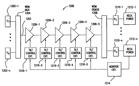
Fig. 12 illustrates an alternative embodiment of the present invention in
which the
attenuators included in a chain of amplifiers are adjusted substantially
simultaneously so that
the power associated with each optical signal output from the chain is
substantially the same.
In particular, Fig. 12 illustrates a WDM system 1200 comprising a plurality of
transmitters
Tr, to Tr~ (1202-1 to 1202-n) each of which emitting one of a plurality of
optical signals.
Each of the plurality of optical signals are at a respective one of a
plurality of wavelengths.
The optical signals are output to and combined, using a conventional WDM
multiplexer
1204, onto an optical communication path 1203, comprising, for example, an
optical fiber. A
chain of optical amplifiers 1206-1 to 1206-S are coupled in series along
optical
communication path 1203. The optical amplifiers can have a structure similar
to that of any
CA 02301825 2000-02-18
WO 99/62186 PCTIUS99/10879
one of optical amplifiers discussed above, including an optical attenuator
coupled between
first and second segments of active optical fiber. A WDM demultiplexer 1208 is
coupled to
optical communication path 1203 at the end of the amplifier chain. Each of the
outputs of
WDM demultiplexer 1208 are coupled to a respective one of receivers 1210-1 to
1210-n,
which convert the optical signals to corresponding electrical signals.
Received power
modules 1212-I to 1212-n sense these electrical signals and determine the
received optical
power and/or signal to noise ratio associated with each optical signal. The
received power
modules supply power level signals corresponding to the received optical
powers to monitor
circuit 1214, which determines whether the received power levels are
substantially equal. If
not, monitor circuit 1214 outputs an adjustment signal to tilt control
circuits 1216-1 to 1216-
5. In response to the adjustment signal, each of tilt control circuits 1216-1
to 1216-S outputs
a corresponding attenuation control signal to the attenuators in amplifiers
1206-1 to 1206-5,
thereby adjusting the output powers of the optical signals supplied from each
of these
amplifiers. Received power modules, in turn, detect the new optical power
levels and supply
new power level signals to monitor circuit 1214. Monitor circuit 1214
typically continues to
output adjustment signals to tilt control circuits 1216-1 to 1216-5, thereby
maintaining
substantially equal power levels for each optical signal.
While the foregoing invention has been described in terms of the embodiments
discussed above, numerous variations are possible. Accordingly, modifications
and changes
such as those suggested above, but not limited thereto, are considered to be
within the scope
of the following claims.
16