Note: Descriptions are shown in the official language in which they were submitted.
CA 02302004 2000-03-22
METHOD AND SYSTEM FOR ACHIEVING CARRIER FREQUENCY
SYNCHRONIZATION IN HIGH SPEED RECEIVERS
FIELD OF THE INVENTION
The present invention relates to a method and system for achieving Garner
frequency synchronization in a high speed receiver. In particular, the present
invention relates
to the carrier recovery loop in a high-speed digital demodulator that
compensates for the phase
and frequency offsets that are present in the complex baseband signal
recovered from the
receiver.
BACKGROUND OF THE INVENTION
In modern digital receivers the digital complex baseband signal recovered from
the analog-to-digital converter invariably contains residual carrier frequency
errors due to
mismatches between the transmit and receive local oscillators. These residual
Garner errors must
be removed before the baseband signal can be fizrther processed and outputted.
One of the prior
art schemes used for correcting this residual Garner error is a carrier
recovery loop circuit that
provides compensating feedback phase and frequency offsets to the corrupted
complex baseband
signal. Figure 1 illustrates the interconnectivity of such a Garner recovery
loop between an
Equalizer and an Air Interface Processor.
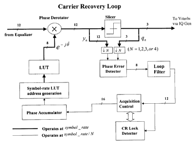
As further shown in Figure 2, a typical carrier recovery (CR) loop consists of
the
following five main components: a phase derotator and dicer, a phase error
detector, a loop filter,
a carrier acquisition control, and the Sine and Cosine Look-Up Table (LUT).
The CR loop will
remain inactive following power-up until the Air Interface Processor (AIP) in
Figure 1 gives the
carrier- synchronization-enable signal. The carrier loop works in
collaboration with the equalizer.
The AIP activates the CR loop once the Equalizer Constant Modulus Algorithm
(CMA) mode
has converged sufficiently. It is assumed that the frequency offset
encountered by the CR loop
is in the order of ~5% of the highest symbol rate of the digital demodulator.
The carrier loop
can operate at a rate of one sample per symbol or at a reduced rate as
programmed by the Air
Interface Processor. In lower data rate applications where the equalizer is
not required, the
equalizer taps will be bypassed, however the dicer will still continue to feed
the quantized
decisions ( qn ) to CR loop. Typically, the input ( y" ) to the dicer has a
word length of 12-bits and
-1-
CA 02302004 2000-03-22
the output ( qn ) is 3-bits wide. Both yn and qn feed the CR sub-system
When the initial frequency offset encountered by the carrier recovery loop is
in
the order of ~ 5% of the symbol rate, the CR loop cannot always lock on to,
and compensate
for, the incoming offset frequency in an unaided fashion. Therefore, the
following acquisition
technique has been added in prior art designs to achieve better carrier lock.
The frequency of
the VCO is swept linearly across the range spanning the maximum frequency
offset
encountered by the receiver. This is done by feeding a linearly changing dc-
voltage to the
output of the loop filter of Figure 2 prior to the phase accumulator. When the
VCO frequency
and the residual offset frequency at the phase derotator input coincide, the
Garner loop will
lock, and the lock detector indicates to the acquisition control unit to
freeze the do sweep
value. The CR loop enters tracking mode at this point. Figure 3 illustrates
the Garner
acquisition process of a typical carrier recovery loop sub-system.
In a high-speed receiver system, hardware realization of the multipliers and
adders used in the CR sub-system can produce pipeline delays that are based on
the number
of hardware clock cycles available for performing computations. Given the
maximum
operating clock frequency of the system, we have a limited number of hardware
clock cycles
between consecutive data samples at the higher data rates. For instance, at
data rates of 155
Mbits per second, the maximum clock frequency becomes close or equal to the
data
sampling-rate. Each hardware multiplication and addition operation in the
carrier recovery
feedback loop will therefore introduce pipeline delays. The presence of such
delays in the
feedback loop introduces instabilities in the Garner acquisition scheme due to
the addition of
unwanted poles in the closed loop system response. When there is an excessive
number of
delay present in the feedback loop, the Garner loop will not be able to
achieve Garner lock
even with the aided acquisition scheme.
(1) 'Self recovering Equalization and Carrier Tracking in Two Dimensional Data
Communication Systems'. Dominique N. Godard. IEEE Transactions on
Communications, Vol. COM-28, No. 11, November 1980. pp 1867-1875.
(2) 'Garner Recovery for Blind Equalization', Neil K. Jablon, IEEE ICASSP
Rec.,
May 23-26 1989.
(3) 'Joint Blind Equalization, Garner Recovery, and Timing Recovery for High-
order
QAM signal Constellations', Neil K. Jablon, IEEE Transactions on Signal
Processing,
-2-
CA 02302004 2000-03-22
Vol. 40, No. 6 June 1992.
(4) 'Blind Carner Phase Acquisition for QAM Constellations', Costas N.
Georghiades,
IEEE Transactions on Communications, Vol. 45, No. 11, November 1997.
It is therefore desirable to provide a technique for alleviating the adverse
effects of pipeline delays in the carrier recovery loop. It is further
desirable to provide a .
SUMMARY OF THE INVENTION
It is an object of the present invention to provide an improved method and
system
for carrier recovery in a high speed receiver.
In a first aspect, the present invention provides a frequency compensation
method
for a receiver, comprising the steps of:
(i) reducing a sampling rate at an input of a phase error detector by a
predetermined
factor; and
(ii) reconstructing the sampling rate by extrapolating at a look up table.
BRIEF DESCRIPTION OF THE DRAWINGS
Preferred embodiments of the present invention will now be described, by way
of example only, with reference to the attached Figures, wherein:
Figure 1 is a block diagram showing the prior art of the interconnectivity
between an equalizer, an air interface processor and a carrier recovery sub-
system;
Figure 2 is a block diagram of a prior art Garner recovery loop;
Figure 3 is a flow chart showing the Garner acquisition process in a prior art
Garner recovery loop;
Figure 4 is a block diagram of the carrier recovery sub-system according to
the
present invention;
Figure 5 is a block diagram of the look up table address block according to
the
present invention;
Figure 6 is a flow diagram showing the phase accumulator gradient calculations
according to the present invention;
Figure 7 is a flow diagram showing the multiplexing of the N addresses to the
look up tables according to the present invention.
-3-
CA 02302004 2000-03-22
DETAILED DESCRIPTION OF THE INVENTION
In order to alleviate the adverse effects of pipeline delays on the carrier
recovery loop in high data rate systems, the present invention employs a
combination of
reduced sampling rate at the phase detector and an extrapolation method for
reconstructing
the sampling rate to the original symbol rate at the look up table. This is
accomplished as
follows:
The input to the phase error detector is down-sampled by a factor of
N (N =1,2,3, or 4) , thus causing the Garner synchronization loop to run at
the lower rate of
symbol _ rate l N . At this lower operating rate, more hardware clock cycles
are available for
computations between successive samples within the Garner loop. The net effect
is that the
pipeline delays seen by the feedback loop will be reduced. The carrier
recovery loop is
operated at the reduced rate until Garner lock is achieved. Using combined
down-sampling
and acquisition control techniques, it is possible to handle up to a
predetermined maximum
number of pipeline delays in the Garner feedback loop. Based on the highest
operating clock
frequency, it is necessary that the selection of down-sampling factor be based
on the symbol
transmission rate such that the total number of pipeline delays seen by the
feedback loop does
not exceed the maximum allowable delay.
For receivers operating at lower incoming data rates, reduced sampling is not
necessary because more hardware clock cycles are available for computations
between
samples, therefore the carrier loop does not need to be run at a reduced rate.
While the technique of reducing the symbol rate alleviates the pipeline delay
in the CR loop, it creates another problem in closing the recovery loop. Since
the phase
derotator and dicer must always operate at the symbol rate, it is necessary
that the reduced
symbol rate in the look up table be reconverted to the original symbol rate.
This is performed
by an extrapolation scheme between the Phase Accumulator and LUT that
regenerates the
carrier phase/frequency correction for the phase derotator at the original
symbol rate.
Since the phase derotator and Slicer need to work at the symbol rate, it is
necessary that the Sine and Cosine look-up tables also read at the original
symbol rate. The
present invention corrects this problem by implementing an extrapolation
technique at the
output of the Phase Accumulator that reconstructs the reduced sample rate to
the original
-4-
CA 02302004 2000-03-22
symbol rate at the look-up tables.
The down-sampled Garner feedback loop is run until the lock detector decides
that carrier lock has been achieved. At this point, the phase accumulator
output displays a
constant slope that is proportional to the carrier offset encountered by the
loop. To restore the
original symbol rate, the current value of the Phase Accumulator output is
extrapolated in
order to generate N -1 more addresses for the LUT between consecutive output
samples
from the Phase Accumulator. This procedure is shown in Figures 5, 6, and 7.
The phase accumulator output gradient computation block operates at
symbol _ rate l N . Once, a slope value has been computed, the additional N-1
phase
accumulator outputs are obtained by adding the offset values to the current
phase accumulator
output as shown. The N phase accumulator outputs are reformatted to form N
look-up table
addresses. These N look-up table addresses are then selected consecutively by
the Mux block
to address the LUT. The Mux select signal operates at the symbol rate.
In summary, for high data rate receivers, the present invention provides a
combination of down-sampling and extrapolation methods in a Garner recovery
sub-system to
run the carrier recovery loop at a reduced rate while operating its phase
derotator and dicer at
the symbol rate. The total pipeline delay as seen by the Garner loop is thus
reduced. This in
turn allows for more efficient correction of residual Garner frequency errors
present in the
complex baseband signal. The down-sampling rate can be programmed for
different settings
based on the operating data rate of the demodulator
The above-described embodiments of the invention are intended to be examples
of the present invention. Alterations, modifications and variations may be
effected to the
particular embodiments by those of skill in the art, without departing from
the scope of the
invention which is defined solely by the claims appended hereto.
-5-