Note: Descriptions are shown in the official language in which they were submitted.
- ' CA 02302128 2000-06-O5
BERGZ465/C2363 ,. PATENT
ELECTRICAL CONNECTOR FOR REDUCING ELECTRICAL CROSSTALK
AND COMMON MODE ELECTROMAGNETIC INTERFERENCE
FIELD ~F THE INVENTION
The present invention relates to electrical connectors and, more particularly,
5. to receptacles for modular jacks for use in telecommunications equipment.
BACKGROUND OF THE INVENTION
Modular jacks for connecting telecommunications equipment are used for two
broad categories of signal transmission: analog (voice) and digital (data)
transmission. While
these categories overlap somewhat since digital systems may be used for voice
transmission,
- there is a significant difference in the data rates transmitted by each type
of system. A low
speed system ordinarily transmits at data rates from about 10 to 16 megabits
per second
(Mbps), while a high speed system transmits at data rates of 155 Mbps or
higher. Often, high
speed installations are based on asynchronous transfer mode transmission and
utilize shielded
and unshielded twisted pair cables.
1 S With recent increases in the speed of data transmission, requirements for
reduction or elimination of crosstalk have become important for electrical
conncctors.
Crosstallc is a phenomena that occurs when a part of the electromagnetic
energy transmitted
through one of multiple conductors in a connector causes electrical currents
in the other
conductors. Another problem is common mode electromagnetic interference or
noise. Such
common mode interference is often most severe in conductors having the same
length, and
CA 02302128 2000-06-OS
....
BERG2465/C2363 - 2 - .. PATENT
occurs when a parasitic signal induced by electrostatic discharge (~SD),
lightning or
simultaneous switching of semiconductor gates arrives in an adjacent
electrical node through
multiple conductors at the same time.
Another requirement driving telecommunication connector design is that the
telecommunications industry has reached a high degree of standardization in
modular jack
design. Outlines and contact areas are essentially fixed and must be
interchangeable with
other designs. It is, therefore, important that any novel modular jack
substantially allow the
use of conventional parts or tooling in its production.
A solution to the above-noted problems is proposed in United States Patent No.
5,599,209, to Betopolsky, the inventor herein, entitled, "Method of Reducing
Electrical
Crosstalk and Common Mode Electromagnetic Interference and Modular Jack for
Use
Therein" ("Betopolsky '209'x. This solution was proposed to reduce crosstalk
and common
mode electromagnetic interference in a modular j ack by: (a) separating round
wire conductors
into two groups that are positioned in a distinct, separate area in the
modular jack; (b)
increasing the distance between adj scent conductors; (c) reducing the common
length between
adjacent conductors; and (d) using significantly different lengths for
adjacent conductors. In
the Belopolsky '209 connector, a first plurality of round wires extends in a
common vertical
plane from the bottom wall of the jack housing across the open rear end to the
top wall and
then extend horizontally forward and then angularly downwardIy and rearwardly
back toward
the rear open end. A second plurality of wires extends first in a common
vertical plane from
- the bottom wall across' only a part of the rear open end and then extends
obliquely,
horizontally and upwardly toward the open front end. The downwardty extending
oblique
plane of the first plurality of wires and upwardly extending oblique plane of
the second
plurality of wires have a common length between 0.8 inch to 1.0 inch, while
the length of the
horizontal section of the first group of wires is relatively much longer being
preferably 0.6
inch to 2.0 inch.
While the Belopolsky '209 modular jack is a vast improvement over the prior
art modular jack cQt~nectors, there is still a need fQr a madulaur, jack which
further reduces
crosstalk in telecommunications equipment. There is also a need for a modular
jack which
wilt further . reduce common mode electromagnetic interference in
telecommunications
equipment. Particularly, there is a need for a modular jack_connector that
meets or exceeds
CA 02302128 2000-06-OS
BERG2465/C2363 - 3 - ~. ' PATENT
Category 5 requirements. There is also a need for such an improved modular
jack to be
interchangeable with prior art modular jacks and to be manufactured using
conventional parts
and tooling. The present invention provides such a solution.
SUMMARY OF THE INVENTION
S The present invention is directed to insulative inserts and conductive leads
that
may be used in fabricating modular jack connectors. The inserts
include.conductors having
a rectangular cross section. In accordance with a first aspect of the
invention, a first insert
includes a first and second plurality of conductive leads that extend across a
top wall in first
and second common planes toward a front end. A first group of conductive leads
form a
terminal edge by extending toward the rear end of the first insert in a first
common oblique
plane. A second group of conductive extends angularly toward the front end
from the second
common plane in a second common oblique plane to form a second terminal edge
which
extends beyond the first terminal edge. A third group of leads may be provided
that extend
across portions of the top wall in both the first and second common planes.
The first and
1 S second oblique planes intersect to form a first contact area.
In accordance with another aspect of the invention, a second insert includes a
third and fourth plurality of conductive leads that extend across a top wall
in third and fourth
common planes. A third group of leads forms a terminal edge by extending
toward the rear
end of the second insert in a third common oblique plane. A fourth group of
leads extends
~~ angularly from the fourth common plane toward the front end in a fourth
common oblique
plane to form a fourth terminal edge which extends beyond the third terminal
edge. The third
and fourth oblique planes intersect to form a second contact area.
In accordance with yet another feature ofthe present invention, a modular jack
connector assembly may be assembled from the first and second inserts.
Other features and aspects will be described herein.
BR)<EF DESCRIPTION OF THE DRAWINGS
The foregoing summary, as well as the following detailed description of the
preferred embodiments, is better understood when read in conjunction with the
appended
drawings. For the purpose of illustrating the invention, there is shown in the
drawings an
CA 02302128 2000-06-OS
BERG2465/C2363 - 4 - ~. PATENT
embodiment that is presently preferred, in which like references numerals
represent similar
parts throughout the several views of the drawings, it being understood,
however, that the
invention is not limited to the specific methods and instrumentalities
disclosed. In the
drawings:
Figure 1 is a perspective view of a first insert adapted for use in a modular
jack
assembly;
Figures 2-5 are front, side, rear and top views of the insert of Figure 1 with
a
first arrangement of conductive leads, respectively;
Figures SA-SH are sectional views taken through lines A-A, B-B, C-C, D-D,
. 10 E-E, F-F, G-G, and H-H of Figure 5;
Figures 6-8 are side, rear and top views of the insert of Figure 1 with a
second
arrangement of conductive leads, respectively;
Figures 8A-8B are sectional views taken through lines A-A and B-B of
Figure 8;
Figure 9 is a perspective view of a second insert adapted for use in a modular
jack assembly;
Figures 10-13 are front, side, rear and top views of the insert of Figure 9
with
an arrangement of conductive leads, respectively; and
Figures 13A-13H are sectional views taken through lines A-A, B-B, C-C, D-D,
E-E, F-F, G-G, and H-H of Figure 13;
r . Figure 14 is a perspective view of a modular jack assembly in which the
first
and second inserts of the present invention may be utilized; and
Figure 15 is a sectional view of the modular jack assembly of Figure 14 taken
through lines A-A of Figure 14.
DETAILED DESCRIPTION OF THE PREFERRED EMBODIMENTS
The present invention is directed to novel connector inserts for use in a
~~~u~a~ j~~ ~ssemb~y to p~vide electrical c~~e~t~o~s bexween ~ev~ces,
~e_fenri~g now to
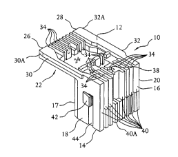
Figure l, there is illustrated a first insert 10 that may be used to fabricate
a modular jack
connector in accordance with an embodiment of the present invention. The
insert 10 includes
a top wall 12, a bottom wall 14, a rear wall 16, a front wall 17, and a pair
of opposed lateral
CA 02302128 2000-06-OS
BERG2465/C2363 . - 5 - .. PATENT
walls 18 and 20. A canterlevered portion 22 is formed extending forward ~f the
front wall 17.
The canterlevered portion 22 has an opening 24 there through. It is noted that
the overall
dimensions of the first insert 10 are sized such that it may be used in an
industry standard
modular jack connector. The material from which the insert 10 is constructed
is preferably
a thermoplastic polymer having suitable insulative properties.
The top wall 12 includes a pair of outer members 26 and 28 that extend the
length of the top wall 12. The outer members 26 and 28 each define a
projecting member 30
and 32 that extends outwardly fi-om the lateral walls 18 and 20, respectively,
to enable the
insert 10 to be positioned and secured within a connector assembly housing
(Figure 14). The
projecting members 30 and 32 each have an angled forward portion 30A and 32A
and extend
rearward on the lateral walls 18 and 20 to a point behind a vertical plane
formed by the front
wall 17.
A plurality of upper grooves 34 are formed within the top wall 12 that extend
from the front of the first insert 10 to the opening 24. The upper grooves 34
are provided such
that electrical conductors may be disposed within the first, insert 10. The
upper grooves 34
preferably have varying depths within the top wall 12 depending on the
particular groove's
position in the top wall 12. Varying the depth of the upper grooves
advantageously reduces
cross talk between conductors disposed within the grooves by placing
predetermined
conductors in different horizontal planes (see, detailed discussion below).
The upper grooves 34 extend rearward from the opening 24 in two general
sections separated by a space 36. A tab 38 is formed in one of the upper
grooves 34. At the
rear of the top wall 12, the upper grooves 34 meet corresponding rear grooves
40 formed in
the rear wall 16. For reasons which will be discussed below, only selected
ones of the upper
grooves 34 have corresponding rear grooves 40. At approximately 40% of the
height of the
rear wall 16, additional rear grooves 40A are provided such that each
conductor placed therein
may be secured within its respective rear groove using a flared portion 61 of
the conductor
(see, Figure 4).
I~~c~ of t~~ ~~terally opposed side w~i~s 18 ~~ ~0 have ~ ta~~ 42 (Armed
thereon that extends outwardly from the side walls. The tab 42 is provided to
enable the first
insert 10 to be mounted within an assembly. An outermost edge of the tabs 42
is formed in
a generally rectangular recess 44 within each of the side walls 18 and 20.
CA 02302128 2000-06-OS
B~RG2465/C2363 ~ - 6 - ~; PATENT
Figures 2-5 and SA-SH illustrate the first insert 10 of tl~e present invention
having electrical conductors 46-60 disposed within the upper and rear grooves
34 and 40. It
is noted that Figures SA-SH illustrate several sections of the first insert 10
of Figure I to
provide additional details to one of ordinary skill in the art. As illustrated
there are preferably
eight conductors disposed within the grooves of the first insert 10. Unlike
prior art solutions
utilizing round wire conductors, the present invention advantageously utilizes
conductors
having a rectangular cross section that are preferably stamped from a single
piece of flat metal
stock (e.g., a lead frame). In accordance with the present invention, the
conductors preferably
have a thickness of 8-16 mils (1/1000 of an inch) and a width of 12-24 mils.
The conductors 46-60 are preferably arranged into three groups within the
upper grooves 34. Each group is positioned in substantially different
horizontal planes (see,
planes A and B in Figures SA-SH). The first group of conductors (64, 52, 56
and 60) are
disposed in plane A and form connector contacts 1, 4, 6 and 8 ("Group A'~. The
second
group of conductors (50 and 54) are disposed in plane B and form connector
contacts 3 and
1 S 5 ("Group B'~. Plane B is preferably approximately 1.3 mm below that of
the plane A. A
portion of the third group of conductors (48 and 58) is disposed in each
ofplanes A and B and
form connector contacts 2 and 7 ("Group C"). Placing the groups of conductors
in different
horizontal planes further reduces crosstalk and common mode ~ interference
versus
conventional arrangements that have conductors disposed within a same plane.
As illustrated in Figure 3 and Figures SA-SH, the three groups of conductors
each have different shapes. The Group A conductors 64, 52, 56 and 60 that form
contacts 1,
4, 6 and 8 are illustrated in Figures SA, SD, SF and SH, respectively. These
conductors are
formed generally as an "L"-shaped section 62 having an angled portion 64. The
angled
portion 64 is formed at an angle of approximately 23-29 ° with respect
to the horizontal
portion of the "L"-shaped section and extends to approximately 3-4 mm below
the bottom of
the canterlevered portion 22 of the insert 10. The conductors 46-60 (contacts)
preferably do
not have a uniform pitch at the front compared to the rear of the insert 10.
For example,
conductors 46-60 could have a pitch of 0.040 inches at the front of the insert
10 and 0.050
inches at the rear of the insert 10.
The Group B conductors that form contacts 3 and 5 are illustrated in Figures
SC and SE. The conductors SO and 54 have a small semi-circular portion
adjacent to the front
CA 02302128 2000-06-OS
BERG-2465/C2363 - 7 - ~. PATENT
wall 1? and extend upwardly at an angle of approximately 11 °. The
terminal end 71 of the
conductors 50 and 54 protrudes from the front of the insert at an angle of
approximately 23 °.
The Group C conductors 48 and 58 that form contacts 2 and 7 are illustrated
in Figures SB and SG, respectively. The conductors each include a "stitched"
portion 70 in
plane A, extend outwardly from the front wall 17, and then upwardly from the
front wall 17
at an angle of approximately 11 ° with respect to the horizontal. A
terminal end 71 of the
conductors 48 and 58 protrudes from the front of the first insert 10
approximately 1-2 mm at
an angle of approximately 23 °.
As illustrated in Figure 3, each of the conductors 46-60 forms aligned contact
areas 74 that lie substantially within an oblique plane. It is intended that
when a modular j ack
is mated to the conductors 46-60 of the first insert 10, the contacts of the
modular jack
electrically contact their respective conductors 46-60 in the contact area 74.
It is also
preferable to selectively plate the contact area 74 using a multilayered
arrangement of
conductive metals, such as nickel, gold and palladium. For example, the
contact area 74 may
be plated using known means having a 50 microinch layer of nickel covered by a
5-100
microinch layer of gold or palladium.
To filrther reduce crosstalk, it is preferable to reduce the distance that the
conductors 46-60 run in parallel along the top wall 12 and to have a portion
the conductor
occupying the fourth position (groove 34D) extend in parallel and on top of
the conductor
occupying the fifth position (groove 34E). As best illustrated in Figures 4,
S, SD and SE, a
portion of the conductor 52 in the fourth position runs in a parallel
horizontal plane above the
conductor 54 in the fifth position on the top of the first insert 10, and in a
parallel vertical
plane behind the conductor 54 in the fifth position at the rear of the first
insert 10. Also, as
can be understood fi-om Figures SD and SE, the fourth conductor 52 will
conduct current
received from a modular jack in contact therewith upward through angled
portion 64, while
the fifth conductor 54 will conduct current from the modular jack downward
with respect to
the first insert 10. Similarly, as can be understood from Figures 3 and SA-SH,
Group A
conductor that ~c di_sposcd adjacent to conductors of ~roupg ~ and ~ will cach
conduct
current received from a modular jack in contact therewith in opposite
directions. Crosstalk
and interference may be fiuther reduced by conducting current in reverse
directions through
the fi-ontal portions of the conductors.
CA 02302128 2000-06-OS
$ERG2465/C2363 - 8 - .. PATENT
_.__._._ _ ~_ .
In addition to placing the groups ofconductors in differen~ planes and
reducing
the distance they run in parallel along the top of the insert 10, the groups
of conductors
preferably have different horizontal lengths as measured along the top of the
first insert 10.
In the present exemplary arrangement, the group B and C conductors have a
horizontal length
between 20 and 60% of the horizontal length of the group A conductors. In
addition, it is
preferable to have the horizontal portion of the Group B conductors in a plane
below that of
the corresponding portion of the Group C conductors. Further, it is preferable
to have the tail
portions 72 of the conductors exit the first insert 10 in different planes. As
illustrated in
Figure 3, the exiting tails 72 are separated into two planes that are
approximately 2.5 mm
apart and each tail is separated from an adjacent tail 72 by approximately
1.27 mm.
Table 1 illustrates test results of crosstalk between contacts in connectors
using
the first insert 10 of the present invention having the arrangement of
conductors as noted
above in Figures 3-5 and SA-SH, with respect to the Category 5 Requirement.
Table 1
Item - Near End Crosstalk, dB 00 MHz
@ 1
1/2 1/2-4/51/2-7/8 3/6-4/S 4/5-7/8 3/6-7/8
-3/6
Sample 46.3 46.2 63.3 46.9 43.6 50.1
1 ~
Sample 45 52.1 53.3 41.2 45.9 45.3
2
Sample 50 43.5 52 42.2 46 45.8
3
Cat.S 40.0 40.0 40.0 40.0 40.0 40.0
_ R 't
Figures 6-8 and 8A-8B illustrate the first insert 10 of the present invention
having a second arrangement of electrical conductors 76-90 disposed therein.
As illustrated
there are preferably eight conductors disposed within the first insert 10 in
accordance with the
second arrangement. The conductors 76-90 are preferably arranged into two
groups (Groups
D and E). Group D includes conductors 76, 82, 86 and 90 disposed in plane D
thaf form
connector contsota I, 4, 6 and 8. C3roup E includes oonductora 78, 80, 84 and
88 diapoaed in
plane E that form connector contacts 2, 3, S and 7. Plane E Is pYeferably 1.3
mm below that
of the plane D. As in the example above according to the first arrangement of
conductors, the
conductors 76-90 have a rectangular cross section. The conductors 76-90
(contacts)
CA 02302128 2000-06-OS
BERG2465/C2363 - 9 - .~. PATENT
preferably do not have a uniform pitch at the front compared to the rear~of
the insert 10. For
example, conductors 76-90 could have a pitch of 0.040 inches at the front of
the insert 10 and
0.050 inches at the rear of the insert 10.
As illustrated in Figures 6 and 8A-8B, the two groups of conductors have
differing shapes to reduce crosstalk and common mode interference. The Group D
conductors
76, 82, 86 and 90 that form connector contacts 1, 4, 6 and 8 are illustrated
in Figure 8A.
These conductors have a substantially similar structure to those of Group A
described with
reference to Figures SA, 5D, 5F and 5H, and will not be described in detail.
The Group E conductors 78, 80, 84 and 88 that form connector contacts 2, 3,
S and 7 are illustrated in Figure 8B. The conductors 78, 80, 84 and 88 each
include a
"stitched" portion 92 and extend upwardly from the front wall 17 at an angle
of approximately
11 ° with respect to the horizontal. The terminal end 91 of the
conductors 78, 80, 84 and 88
terminates approximately 0.34 mm from the fi-ont of the first insert 10.
As illustrated in Figure 6, each of the conductors 76-90 forms aligned contact
areas 94 that lie substantially within an oblique plane. It is intended that
when the modular
jack is inserted into an assembly containing the insert 10 according to the
second arrangement
of conductors, the contacts of the modular j ack electrically contact their
respective conductors
76-90 in the contact area 94. Also as in the example above, the contact area
94 preferably has
a multilayered plated region.
As noted above, to filrther reduce cross talk, it is preferable to reduce the
distance that the conductors 76-90 run in parallel along the top wall 12, and
have a portion of
the conductor occupying the fourth position (groove 34D) extend in parallel
and on top of the
conductor occupying the fifth position (groove 35D) of the first insert 10. As
best illustrated
in Figures 7, 8, 8A and 8B, a portion of the conductor 82 in the fourth
position runs in a
parallel horizontal plane above the conductor 84 in the fifth position on the
top of the first
insert 10, and in a parallel vertical plane behind the conductor 84 in the
fifth position at the
rear of the first insert 10. Also, as can be understood from Figures 8A and
8B, the fourth
conductor will conduct current received tom a m~du~~r jerk i~ cQnt~c_t_
therewith upward
through angled portion 64, while the fifth conductor will conduct current from
the modular
jack downward with respect to the first insert 10: Similarly, it is noted that
conductors of
.i
CA 02302128 2000-06-OS
B,ERG24b5/C23b3 -10 - ,, PATENT
Group D that are adjacent to conductors of Group E will each conduct current
received from
a modular jack in contact therewith in opposite directions.
In addition to placing the groups ofconductors in different planes and
reducing
the distance they run in parallel along the top of the insert 10, the groups
of conductors
preferably have different horizontal lengths as measured along the top of the
first insert 10.
For example, the group E conductors have a horizontal length between 20 and
60% of the
horizontal length of the group D conductors. Further, it is preferable to have
the tail portions
72 of the conductors exit the first insert 10 in different planes. As
illustrated in Figure 6, the
exiting tails 72 are separated into two planes that are approximately 2.5 mm
apart and each
tail is separated from an adjacent tail 72 by approximately 1.27 mm.
Figure 9 illustrates a second insert 100 that may be used to fabricate a
connector in accordance with the present invention. The second insert 100
includes a first top
wall 102,'a second top wall 104, a bottom wall 106, a rear wall 108, a front
wall 110, aild a
pair of opposed lateral walls 112 and 114. A canterlevered portion 116 is
formed extending
forward of the front wall 110 and includes the first top wall 102 and a
portion of the second
top wall 104. The material from which the second insert 100 is constructed is
preferably a
thermoplastic polymer having suitable insulative properties.
The first top wall 102 defines a plurality of angled grooves 118 (having an
angle of approximately 15 °) and first upper grooves 120. The second
top wall 104 is
approximately 2.2 mm above the first top wall 102 and defines second upper
grooves 122.
The first and second upper grooves are provided such that electrical
conductors may be
disposed within the second insert 100 (to be described in greater detail
below). The second
upper grooves 122 continue rearward from the front edge of the second top wall
104 and meet
corresponding rear grooves 124 fortried in the rear wall 108. At approximately
28% of the
height of the rear wall 108, the rear grooves 124 are shaped such that each
conductor may be
secured using a flared portion 61 within its corresponding groove in the rear
wall 108 (see,
e.g., Figure 12).
Each of the laterally opposed lateral walls 112 and 114 have formed thereon
a first tab 126 and second tab 127 that extend outwardly from the opposed
lateral walls 112
and 114. The tab 126 may be used in mounting the second insert 100 within a
modular jack
assembly.
CA 02302128 2000-06-OS
$ERG2465/C2363 -11 - ... PATENT
Figures 10-13 and 13A-13H illustrate the second insert 100 of the present
invention having electrical conductors 128-142 disposed therein. It is noted
that Figures 13A-
13H illustrate several sections of the second insert 100 of Figure 9 to
provide additional
details to one of ordinary skill in the art. As illustrated there are
preferably eight conductors
disposed within the second insert 100. The conductors each have a rectangular
cross section
and are preferably stamped from a single piece of flat metal stock (e.g., a
lead frame). The
conductors preferably have a thickness of 8-16 mils (1/1000 of an inch) and a
width of 12-24
mils. The conductors 128-142 (contacts) preferably do not have the same pitch
at the front
compared to the rear of the insert 100. For example the conductors may have a
pitch of 0.040
inches at the front of the insert 100 and 0.050 inches at the rear of the
insert 100.
As best shown by Figures 10 and 11, the conductors 128-142 are preferably
arranged into two groups, with selected members of the first group being
positioned in
different horizontal planes (illustrated as planes F and G). The first group
(Group F) includes
conductors 128, 134 and 142 that form contacts 1, 4 and 8 that are disposed in
plane F,
whereas conductors 130 and 138 that form contacts 2 and 6 are located in plane
G. Plane G
is approximately 3.5 mm below that of plane F. The second group (Group G) of
conductors
132, 136 and 140 that form contacts 3, 5 and 7 are located in plane G.
As illustrated in Figure 11 and Figures 13A-13H, the two groups ofconductors
preferably have differing shapes to reduce crosstallc and common mode
interference. The
conductors 128, 130, 134, 138 and 142 that form contacts 1, 2, 4, 6 and 8 are
illustrated in
Figures 13A,13B,13I),13F and 13H, respectively. These conductors
128,130,134,138 and
142 are formed having a generally "L"-shaped section 144 and an angled portion
146. The
angled portion 146 is formed at an angle of approximately 23-29° with
respect to the
horizontal portion of the "L"-shaped section. The conductors 132, 136 and 140
that form
contacts 3, 5 and 7 are illustrated in Figures 14C, 14E and .14G,
respectively. These
conductors also have an "L"-shaped section 148 and a forward downward portion
150 (angled
at approximately 11 °). An "S"-shaped bend follows the downward portion
150 and the
tern~~nal ends of the conductors 132; t 36 and 140 extend .outward of the
front of the second
insert 100 at approximately an 11 ° angle to form a terminal end 141.
As illustrated in Figure 1l, each.:of the conductors 128-142 form aligned
contact areas 152 that lie substantially within an oblique plane. It is
intended that when the
CA 02302128 2000-06-OS
B,ERG2465/C2363 , -12 - ~; PATENT
modular jack is inserted into a modular jack connector assembly utilizing the
second insert
100, the contacts of the modular jack electrically contact their respective
conductors 128-142
in the contact area 152. It is also preferable to use selective plating of the
contact area 152 of
the conductors 128-142 using a multilayered arrangement of conductive metals,
such as
nickel, gold and palladium. For example, the contact area may be plated using
known means
having a 50 microinch layer of nickel covered by a 5-100 microinch layer of
gold or
palladium.
To further reduce crosstalk, it is preferable to reduce the distance that the
. conductors 128-142 run in parallel along the second top wall 104 and to have
the fourth
conductor 134 overlap the fifth conductor 136. As best illustrated in Figure
13, a portion of
the conductor 134 in the fourth position runs in a parallel horizontal plane
above the conductor
136 in the fifth position for a portion of the second top wall 104. Also, as
can be understood
from Figures 11 and 13A-13A, the fourth conductor will conduct current
received from a
modular jack in contact therewith downward through angled portion 146, while
the fifth
1 S conductor will conduct current from the modular jack generally upward.
Similarly, adj acent
conductors from Groups F and G will each conduct current received from a
modular jack in
contact therewith in opposite directions to further reduce crosstalk. Further,
it is preferable
to have the tail portions 72 of every other conductor exit the second insert
100 in different
planes. As illustrated in Figure 11, the exiting tails 72 are separated into
two planes that are
approximately 2.5 mm apart and each tail is separated from an adjacent tail 72
by
approximately 1.27 mm.
Referring now to Figure 14; there is illustrated a modular jack connector
assembly 200 which utilizes the inserts of the present invention. In
accordance with a feature
of the present invention, the first and second inserts 10 and 100 may be
stacked together and
mounted within the modular jack connector assembly 200 to form a double deck
assembly.
Figure 14, illustrates such an exemplary 8 port double deck modular jack
assembly utilizing
the first and second inserts 10 and 100. Such an assembly may be mounted to,
e.g., a printed
eire~t board 24~ to provide co~lnect~ons between various co~vunieations-
related eq~ipm~nt.
The assembly 200 includes a plurality of modular jack connectors 204 that are
adapted to
receive modular jacks such as an industry standard~RJ45 modular jack having 8
conductors.
Figure 15 illustrates a cross-sectional diagram taken along line A-A of Figure
14. It is noted
I
r
CA 02302128 2000-06-OS
BERG2465/C2363 -13 - ., PATENT
that the arrangement of the conductors within the first and second inserts 10
and 100
advantageously reduces crosstalk and common mode interference such that
shielding (i.e., a
middle ground) is not required between the inserts 10 and 100 to reduce
crosstaIk to
acceptable levels, as evidenced by Table 2 below.
Table 2
Pair combinationNo middle shield With middle shield
(dB) (dB)
1/2-1/2 67 72
1/2-4/5 60 61
1/2-3/6 65 68
7/8-1/2 56 55
4%5-4/5 62 66
3/6-3/6 45.3 48.4
4/5-3/6 66 64
It will be appreciated that there has been described a method of reducing or
eliminating crosstalk as well as common mode electromagnetic interference and
a modular
jack for use therein. It will also be appreciated that this modular jack is
interchangeable with
conventional modular jacks and can be manufactured easily and, inexpensively
with
conventional pads and tooling. Further, the present invention provides for an
overall design
that allows the incorporation of a shallower latch.'
The present invention may be employed in other specific forms without
departing~from the spirit or essential attributes thereof. For example, any
number ofmaterials
may be used in manufacturing the disclosed latch member. While the invention
has been
described and illustrated with reference to specific embodiments, those
skilled in the art will
recognize that modification and variations may be made without departing from
the principles
of the invention as described herein above and set forth in the following
claims. For example,
a number other than eight conductive leads may be provided as necessary within
the inserts.