Note: Descriptions are shown in the official language in which they were submitted.
CA 02302290 2000-02-29
WO 99110914 PCTIUS98/17933
INFRARED EMISSIVE MODULE
BACKGROUND OF THE INVENTION
I. Field of the Invention.
The present invention relates generally to the field of heat emitting
devices. More particularly, the present invention relates to a unitary,
composite,
flexible, laminated infrared emissive module having redundant circuitry that
is
well suited for use as an infrared target.
II. ~ Description of the Related rt.
It is well known that objects having a surface temperature greater than
absolute zero are capable of dissipating energy into the environment in the
form of infrared radiation. Under certain circumstances, devices which emit
infrared radiation can be utilized to heat objects or structures and can be
utilized as a target for weaponry having infrared detection devices that "see"
infrared emitting device's thermal signature.
1
CA 02302290 2000-02-29
WO 99110914 PCT/US98/17933
In U.S. Patent Number 4,250,390, Ellis et al. describe a solid state
electrically conductive laminate. The laminate has a substantially continuous,
electrically conductive layer of substantially uniform thickness comprised
mainly
of carbon that emits infrared radiation when an electric current is passed
through it. This layer is specifically described as a homogeneous blend of
about 60g'o to about 9896 by weight of graphite, about 1.5% to about 2096 by
weight of manganese dioxide, and about 0.5% to about 20% by weight of zinc
oxide. The electrically conductive layer is described as being applied to a
flexible binder by silkscreen application. A pair of busbars having opposite
electrical polarity are placed in contact with the electrically conductive
layer in
varying arrangements. However, the busbars are not in a networked series-
parallel power and ground plane circuit arrangement and if one of the busbars
is dissected, major portions, if not all, of the electrically conductive layer
cease
to emit infrared radiation. The electrically conductive layer is disposed
between
a pair of barrier layers, which are additionally disposed between a pair of
insulating layers.
Rosa, a co-inventor of U.S. Patent Number 4,250,390 described above, in
U.S. Patent Numbers 4,422,646, 4,546,983 and 4,659,089 describes infrared
targets likewise having a substantially continuous, electrically conductive
layer
of substantially uniform thickness comprised mainly of carbon that emits
2
CA 02302290 2000-02-29
WO 99/10914 PCT/US98/17933
infrared radiation when an electric current is passed through it. The
electrically conductive layer is not well described except that it is
comprised
mainly of carbon. This device also has a pair of busbars of opposite
electrical
polarity, except that each busbar is respectively connected at each end
thereof
to its mating electrical pole of an electrical source. This device likewise
does
not have a networked series-parallel power and ground plane circuit
arrangement, arid if one of the busbars is dissected, major portions, iF not
all,
of the electrically conductive layer cease to emit infrared radiation. As a
target,
this device's usefulness is limited, because once the busbars have received a
relatively few number of "hits" by a projectile fired by a weapon, it ceases
to
produce an even thermal signature. It appears that this device is improved
over the device described by Ellis et al. only in that both ends of each
busbar
is connected to a respective pole of an electrical power sour ce and does not
leave
barrier layers.
3
CA 02302290 2000-06-16
SUI~iARY OF THE INVENTION
In accordance with the present invention and the contemplated
problems which have and continue to exist in this field, this
invention seeks to provide an infrared emissive module that is new,
unique and improved over the prior art.
Further the present invention seeks to provide a networked
series-parallel power and ground plane circuit to provide even
distribution of an electrical current across an electrically
conductive layer of the infrared emissive module.
Yet further the present invention seeks to provide a flexible
electrically conductive layer that is a composite of a
fluoroelastomer and carbon, and the composite is mainly the
fluoroelastomer.
Still further the present invention seeks to provide an
infrared emissive module that can be utilized as a target for live
fire exercises that utilize equipment which can view an infrared
emission.
This invention accomplishes the above and other aspects and
overcomes the disadvantage of the prior art by providing an
infrared emissive module that is simple in design and construction,
inexpensive to fabricate, and easy to use.
4
CA 02302290 2000-06-16
The invention in a broad aspect provides a unitary, composite,
laminated infrared emissive module connectable to an electrical
power source having two, oppositely-charged electrical poles,
comprising an electrically insulating carrier layer, an
electrically conductive layer disposed on the carrier layer, the
electrically conductive layer generating an infrared emission when
an electric current is passed therethrough, and a power and ground
plane circuit operatively connecting the electrically conductive
layer to the electrical current.
The invention in another broad aspect provides a unitary,
composite, laminated infrared emissive module, comprising an
electrically insulating carrier layer, an electrically conductive
layer comprising carbon and a fluoroelastomer disposed on the
carrier layer and generating an infrared emission when an electric
current is passed therethrough, and an electrical circuit
operatively connecting the electrically conductive layer to the
electrical current.
More particularly, the module comprises an electrically
insulating carrier layer, an electrically conductive layer mounted
to the carrier layer, an electrically insulating top layer mounted
to the carrier and electrically conductive layers on one side of
the carrier layer and an electrically insulating bottom layer
mounted to the other side of the carrier layer to form a unitary,
composite, laminated infrared emissive module. The carrier layer
comprises a vinyl film, and the top and bottom layers comprise a
polyester film, which are mounted to the carrier layer by a heat
and pressure sensitive adhesive. The electrically conductive
layer is a flexible composite of a fluoroelastomer and carbon,
wherein the electrically conductive layer is comprised mainly of
the fluoroelastomer and is applied to the carrier layer by spraying
CA 02302290 2000-06-16
to form fibers and atomized particles. Electrical current is
supplied to the electrically conductive layer from an electrical
power source by a networked series-parallel power and ground plane
circuit that provides even distribution of the electrical current
and circuit redundancy enabling the module to continue to function
with little or no change in infrared emission after being
perforated by projectiles.
It is to be understood that the phraseology and terminology
employed herein are for the purpose of description and should not
be regarded as limiting. As such, those skilled in the art will
appreciate that the conception, upon which this disclosure is
based, may readily be utilized as a basis for the designing of
other structures, methods, and systems for carrying out the several
purposes of the present invention. It is important, therefore, that
the claims be regarded as including such equivalent constructions
insofar as they do not depart from the spirit and scope of the
present invention.
Other aspects, advantages and capabilities of the invention
will become apparent from the following description taken in
conjunction with the accompanying drawings showing preferred
embodiments of the invention.
BRIEF DESCRIPTION OF THE DRAWINGS
The invention will be better understood and the above objects
as well as obj ects other than those set forth above will become
apparent when consideration is given to the following detailed
description thereof. Such description makes reference to the
annexed drawings wherein:
6
CA 02302290 2000-02-29
WO 99110914 PCT/US98/17933
Figure 1 is a front elevation view, partially in schematic form, of a
plurality of infrared emissive modules constructed in accordance with the
present invention and arranged to form a typical thermal target silhouette,
particularly that of a tank, including a diagrammatic illustration of an
electrical
power supply and connections thereto;
Figure 2 is a plan view of an embodiment of the present invention with
a networked series-parallel power and ground plane circuit mounted to a
carrier
layer;
Figure 3 is a partial view of an electrically conductive layer mounted to
to the embodiment of Figure 2;
Figure 4 is a partial sectional view of the embodiment depicted in
Figure 3 taken along line 4-4 and looking in the direction of the arrows
illustrating a cross-over;
Figure 5 is an enlarged view of a portion of the electrically conductive
layer;
Figure 6 is a partial view of the embodiment of Figure 2 ;
7
CA 02302290 2000-02-29
WO 99/10914 PCT/US98/17933
Figure 7 is a plan view of another embodiment of the present invention
with the electrically conductive layer mounted to the carrier layer and the
networked series-parallel power and ground plane circuit mounted to the
electrically conductive layer;
5. figure 8 is a partial view of the embodiment of Figure 7;
figure 9 is a plan view of the carrier layer having perforations;
Figure 10 is a front view of the carrier layer of Figure 9 having busbars
mounted thereto; and
Figure 11 is a back view of the carrier Iayer of Figure 9 having connector
to bars of the series parallel power and ground plane circuit mounted thereto.
-I'he reference numbers in the drawings relate to the following:
2 = thermal target
3 = electrical power source
= infrared emissive module
12 = carrier layer
14 = electrically conductive layer
s
CA 02302290 2000-02-29
WO 99/10914 PCT/US98I17933
16 = bottom layer
18 = top layer
20 = networked series-parallel power and ground plane circuit
22 = busbar
24 ~ connector bar
26 = cross-over
28 = insulation layer
30 = connection pad
32 = wire
l0 34 = fiber of electrically conductive layer
36 = interstitial area of electrically conductive layer
38 = grommet
40 = perforated hole
DESCRIPTION OF THE PREFERRED EMBODIMENTS
ror a fuller understanding of the nature and desired objects of this
invention, reference should be made to the following detailed description
taken
in connection with the accompanying drawings. Referring to the drawings
wherein like reference numerals designate corresponding parts throughout the
9
CA 02302290 2000-02-29
WO 99/10914 PCTNS98/I7933
several figures, reference is made first to Figure 1. Figure 1 of the drawings
illustrates a thermal target 2 comprised of a plurality of infrared emissive
modules 10 constructed in accordance with the present invention. Although the
arrangement of infrared emissive modules 10 of Figure 1 provides the thermal
target 2 with a thermal silhouette of a tank, it should be readily apparent
that
the inf rayed emissive modules 10 can be arranged in various configurations to
produce thermal silhouettes of other objects, including people. Additionally,
is should as well be readily apparent that the infrared emissive module 10 can
be utilized as a heat source to provide heat or warmth for most any occasion
or
l0 circumstance where such heating needs apply.
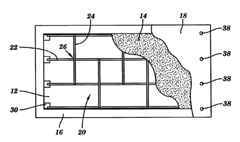
The infrared emissive module 10 comprises a unitary, composite, flexible
laminate. Referring additionally to Figures 2 through fi, the infrared
emissive
module 10 has an electrically insulating carrier layer 12, an electrically
conductive layer 14, an electrically insulating bottom layer 16 and an
electrically
insulating top layer 18. To conduct electricity from an electrical power
source 3
to the electrically conductive layer 12, the module 10 has a networ ked series-
parallel power and ground plane circuit 20 operatively connected to the
electrical power source 3.
l0
CA 02302290 2000-02-29
WO 99/10914 PCT/US98/17933
The carrier layer 12 can be made of any electrically insulating material.
For example, certain metallic alloys are electrically non-conductive and can
be
readily utilized in the present invention. Preferably, the carrier layer 12 is
made of a flexible, flame retardant, electrically insulating material, such as
a
vinyl film. Vinyl, or polyvinyl chloride, film is most preferred because it
provides the module 10 with improved material strength, tear resistance and
flame retardance, which produces a self-extinguishing characteristic.
In the embodiment shown in Figure 2, the networked series-parallel
power and ground plane circuit 20 is mounted directly to the carrier layer 12.
to The circuit 20 has a plurality of busbars 22 and at least one connector bar
24.
The busbars 22 and the connector bars 24 are made of an electrically
conductive material, preferably a flexible electrically conductive material.
Suitable materials for bars 22 and 24 are electrically low-resistive
composites of
carbon dispersed in a suitable cured binder system, silver wire, strip or
tape,
copper wire, strip or tape, aluminum wire, strip or tape, and electrically
conductive pastes. Again, referring to Figures 1 and 2, the busbars 22 are
mounted to the carrier layer 12 substantially equal-distantly from and
substantially parallel to one another to prevent "hot spots" from being
developed by the electrically conductive layer 14. This aides in the
prevention
2o of uneven electrical resistance between a bulbar 22 of one electrical pole
to a
m
CA 02302290 2000-02-29
WO 99/10914 PCT/US98/17933
busbar 22 having the opposite electrical pole. The busbars 22 are arranged so
that the electrical polarity is alternated, as shown in Figure 1. The
connector
bars 24 are provided to operatively, electrically connect busbars having the
same
electrical polarity. In the event the operative electrical connection to the
power
source 3 of a particular busbar 22 is severed, the connector bar 24 continues
to
provide operative electrical connection to the respective pole of the
electrical
power source 3 to the isolated portion of the busbar 22. An intersection of a
busbar 22 of one electrical polarity and a connector bar 24 having the
opposite
electrical polarity is defined as a cross-over 26. An exemplary cross-aver 2fi
is
detailed in Figure 4. Mach cross-over 26 has an electrically-insulating
insulation
layer 28 disposed between the busbar 22 and the connector bar 24 to prevent
current flow. At intersections of busbars 22 and connector bars 24 having the
same electrical polarity, the bars 22 and 24 are electrically interconnected
or
bonded to one another by means of welding, stapling, conductive ink-flexible,
conductive paste, crimping and conductive adhesive, preferably by a conductive
epoxy adhesive, to provide current flow having minimal resistance. The power
and ground connections, described immediately above, can be arranged in
precise redu ndant geometrical patterns that can be repeated such that any
number of opposite polarity paths can be developed to enable the module 10
2o to withstand numerous live fire hits or perforations when used as a target
or
provide numerous circuit redundancies when required in applications where
12
CA 02302290 2000-02-29
WO 99/10914 PGT/US98/17933
thermal heat supplies are critical. At either end of the busbars 22 are
optional
connection pads 30 made of an electrically conductive material to assist in
connecting the busbars 22 to the appropriate pole of the electrical power
source 3.
Because of the redundant circuitry of networked series-parallel power
and ground plane circuit 20, several hits to a single busbar 22 will not
necessarily disable that portion of the module 10, let alone the entire
module 10. Additionally, each module 10 can be quickly repaired on site using
simple tools and inexpensive materials.
Referring again to Figure 1, in order to connect the busbars 22 to the
electrical power source 3, they are provided with external electrical wires
32,
usually having clip connectors (not shown) to grip the module 10 at both ends
of the respective busbar 22. To provide additional redundancy and additional
life to the module 10 when being utilized as a target, wires 32 having the
same
electrically polarity are also connected in series. Additionally, these
connections
can be made by crimping, soldering, brazing or otherwise securing electrical
connections. Particularly shown in Figure 4, another insulation layer 28 is
mounted to the connector bar 24 prior to the addition of the electrically
13
CA 02302290 2000-02-29
WO 99/10914 PCT/US98/I7933
conductive Iayer 14 to prevent electrical contact between the connector bar 24
and the electrically conductive layer 14. The insulation layer 2$ preferably
comprises polyester tape.
Now, referring additionally to Figures 3 through 5, the electrically
conductive layer 14 is mounted to the carrier layer 12 and the busbars 22. The
electrically conductive layer 14 is a composite comprising carbon, or
graphite,
and a fluoroelastomer, preferably a tetrafluoroethylene/vinylidene fluoride
copolymer. It is neither necessary nor desired for the electrically conductive
layer 14 to be mainly comprised of carbon when utilizing the fluoroelastomer.
It has been found that the electrically conductive layer 14 enables the
module 10 to operate and remain flexible in temperature ranges between minus
forty degrees F. (-40 deg. F.) to five hundred degrees F. (500 deg. F.),
resist
oxidation and cure at room temperature. Proper application of the electrically
conductive layer 14 is critical. Preferably, the electrically conductive layer
14
is applied by spraying. In order to retain flexibility, the spray nozzle (not
shown) must be adjusted so that the composite exits the nozzle in a
combination
of atomized particles and fine fiber, or filament, having the consistency
similar
to that of spider web. Referring now to Figures 4 and 5, the electrically
conductive layer 14, after application thereof, has a general thickness of
0.001
inch, but the thickness of the electrically conductive layer 14 is non-
uniform.
14
CA 02302290 2000-02-29
WO 99/10914 PC'T/US98/1'7933
Additionally, the electrically conductive layer 14 has fibers 34, particles
interposed between the fibers, and interstitial areas 36 disposed within the
fibers 34 and particles. Even though the electrically conductive layer 14 has
a
non-uniform thickness, there is an even emission of infrared radiation. There
is an inverse linear relationship between the weight of the electrically
conductive layer and the resulting resistivity, and also between the
laminating
pressure and temperature to which the electrically conductive layer 14 is
subjected. To achieve a lower wattage output, a smaller amount of the
electrically conductive layer 14 is needed. By increasing the thickness of the
electrically conductive layer 14, a greater wattage output occurs. However,
the
electrically conductive layer 14 must be applied so that the fibers 34 and the
interstitial areas 36 are produced as described above to maintain flexibility.
The
fibers 34 are substantially electrically interconnected throughout the
electrically
conductive layer 14. Although the electrically conductive layer 14 will
generate
an infrared emission when it is substantially continuous and has a
substantially
uniform thickness, the electrically conductive layer 14 is brittle, even at
atmospheric conditions. Additionally, bonding between the busbars 22 and the
electrically conductive layer 14 is reduced, causing an increase in electrical
resistance and reduced thermal generation. A suitable composite composition
for spraying has about 8496 to 8596 methyl ethyl ketone by volume as a
solvent,
about 1196 to 12% fluoroelastomer by volume and about 1 to 4.396 carbon by
CA 02302290 2000-02-29
WO 99/10914 PCT/US98/17933
volume. Carbon black may also be dispersed within the composite. Because the
fluoroelastomer has good moisture resistance, the module 10 continues to
function acceptably even after an object has been fired through it.
With continued reference to Figures 2 through 5 and especially Figure G,
the module 10 is protected by the electrically insulating bottom layer 1 G and
top
layer 18. Preferably, the bottom and top layers 16 and 18 are made of a
polyester film. The bottom and top layers 1G and 18 can be of the same
composition as the carrier layer 12. Although any conventional method may be
utilized to affix the bottom and top layers to the carrier and electrically
conductive layers 12 and 14, it is preferred to bond the bottom and top
layers 16 and 18 to the carrier and electrically conductive layers 12 and 14
with
a heat and pressure sensitive adhesive. By pressing and heating the module 10
as the bottom and top layers 16 and 18 are applied, the electrically
conductive
layer I4 has improved electrical contact with the busbars 22 and the top layer
18
bonds directly to the carrier layer 12 through the electrically conductive
layer 14
via the interstitial areas 36, improving the strength, and the tear and
weather
resistance of the module 10 as compared to the prior art.
16
CA 02302290 2000-02-29
WO 99/10914 PCT/US98/17933
To connect the wires 32 to the busbars 22, any standard electrical
connection device may be utilized. In one embodiment, brass spur grommets 38
are anchored into the module 10 thereby making intimate electrical contact
with
the busbars 22.
Referring now to Figures 7 and 8, another embodiment of the present
invention is shown. In this embodiment, the electrical conductive layer 14 is
mounted to the carrier layer I2 before the networked series-parallel power and
ground plane circuit 20 is applied to the module 10. The insulation layer 28
is likewise disposed between the connector bars 24 and the electrically
to conductive layer 14. The remaining features of this embodiment remain the
same as previously described.
Yet, another embodiment is shown in Figure 9 through 11. In this
embodiment, as shown in Figure 9, the carrier layer 12 has perforations 40 at
the locations of the intersections of like polarized busbars 22 and connector
bars 24. Figure 10 shows the busbars 22 disposed on one side of the carrier
layer I2 extending over the respective perforations 40, and Figure 10 shows
the
connector bars 24 disposed on the opposite side of the carrier layer 12
extending from the respective perforations. In this configuration, the
insulation layer 28 between the connector bars 24 and the electrically
conductive
17
CA 02302290 2000-02-29
WO 99/I0914 PCT/US98/I7933
layer 14 is not needed, because the carrier Iayer 14 provides the needed
electrical insulation. The remaining features of this embodiment are the same
as described above. In this configuration, the electrically conductive layer
14
may be applied to the side of the carrier layer 12 having the busbars 22 prior
to the mounting of the busbars 22. The busbars 22 and the connector bars 24
are placed in electrical contact with each other through the perforations 40.
If
there are no perforations, then the busbars 22 and the connector bars 24 are
placed in electrical contact with each other by means of conductive inks,
pastes,
epoxies, adhesives, staples and by sewn metallic threads.
Because of the uniformity provided in the module I0, thermal and visual
signals are identical from module to module. Furthermore, firing conditions
can be duplicated from day to day with the only variable being environmental
conditions. Additionally, because of the modular design, modules 10 are
separate and independent of one another so that damaged to one module, has
no effect on the signal emitted by the remaining interlinked modules 10.
It should be readily apparent that a minimum of two busbars 22 having
opposite polarity are needed to provide an electric current from an electrical
power source 3 to the electrically conductive layer 14.
18
CA 02302290 2000-02-29
WO 99/10914 PCT/US98/17933
Modules 1 U having 8 square feet emissive area made in accordance with
the present invention, have been subjected to a current passed across the
electrically conductive layer I4 to yield the following approximate module
surface temperature increases above atmospheric temperature:
AMPS/ WATT/ TEMP.
VOLTS . FT. SO FT DEG. F./SO.FT.
120 A.C. 0.08 9 4
120 A.C. 0.10 12 '7
120 A.C. 0.13 15 10
120 A.C. 0.15 18 I 3
12 D.C. 0.'75 9 4
12 D.C. 1.00 12 '7
12 D.C. 1.25 15 10
12 D.C. I.5 18 13
With respect to the above description then, it is to be realized that the
optimum dimensional relationships for the parts of the invention, to include
variations in size, materials, shape, form, function and manner of operation,
assembly and use, are deemed readily apparent and obvious to one skilled in
the art, and all equivalent relationships to those illustrated in the drawings
and
2o described in the specification are intended to be encompassed by the
present
invention.
19
CA 02302290 2000-02-29
WO 99/10914 PCT/US98/1'7933
Therefore, the foregoing is considered as illustrative only of the
principles of the invention. Further, various modifications may be made of the
invention without departing from the scope thereof and it is desired,
therefore,
that only such limitations shall be placed thereon as are imposed by the prior
art and which are set forth in the appended claims.