Note: Descriptions are shown in the official language in which they were submitted.
CA 02302493 2000-02-28
WO 00/00876 PCT/US99/14443
APPARATUS AND METHOD FOR REDUCING ENERGY FLUCTUATIONS
IN A PORTABLE DATA DEVICE
Field of the Invention
The invention is related generally to portable data devices, or smart
cards, and more particularly to a method and apparatus for regulating the
energy fluctuations created by circuits thereon.
Background of the Invention
Portable data carriers (i.e., smart cards or chip cards) are known to
include a plastic substrate within which a semiconductor device (i.e.,
integrated circuit --IC) is disposed for processing digital data. This digital
data
may constitute program instructions, user information, or any combination
thereof. Moreover, these devices are known to be operational in a contacted
mode, whereby an array of contact points disposed on the plastic substrate
and interconnected with the semiconductor device is used to exchange
electrical signals between the portable data carrier and an external card
reader, or data communications terminal. Similarly, there exist smart cards
that operate in a contactless mode, whereby a radio frequency (RF) receiving
circuit is employed to exchange data between the card and a card terminal.
That is, the card need not come in physical contact with the card terminal in
order to exchange data therewith, but rather must simply be placed within a
predetermined range of the terminal. Additionally, there exist smart cards
that are alternatively operational in either a contacted mode or a contactless
mode. Such cards are equipped with both RF receiving circuitry (for
contactless operations) as well as an array of contact pads (for contacted
operations), and are commonly referred to as dual mode smart cards.
Whether operating in the contacted or contactless mode, several
problems plague the smart card designer. One such problem involves the
energy fluctuations created by the integrated circuit on the smart card. These
energy fluctuations, which can be caused by common switching noise from a
digital signal processor or by current spikes reflective of processing
activity,
create two somewhat distinct problems during normal smart card operation;
1
CA 02302493 2000-02-28
WO 00/00876 PCT/US99/14443
namely, receiver sensitivity to the switching noise and security breaches, as
next described.
The problem of switching noise is most notable during contactless
operation, whereby sensitive analog circuitry shares a common supply rail
with the signal processing unit. Referring to FIG. 1, a smart card
arrangement 100 includes a substrate 102 for housing the smart card
circuitry. The power node 104 is used to supply power, via supply lines 106
and 108 (Vpp and VSS, respectively), to an optional analog circuit 110 and a
signal processor 112. It should be noted that in contacted operation, the
analog circuit is not required, as the signal processor 112 receives power
directly from an external data communications terminal (not shown).
However, in contactless operation, the analog circuit 110 is present, which
may include sensitive circuitry whose performance degrades in response to
switching noise generated by the signal processor 112. In particular, analog
circuit 110 may be a data recovery circuit and required to recover a data
signal from a power signal that is modulated with 10% amplitude shift keying
(ASK). If the switching noise generated by the signal processor 112 is
allowed to couple to the ASK modulated power signal, the data signal may
become corrupted. Thus, the problem of switching noise must be addressed
in order to improve performance during contactless operations.
Another problem, which exists in both contacted and contactless
modes of operation, stems from the digital signature produced by the signal
processor 112, wherein each data transfer and instruction execution will
typically draw a different amount of energy (e.g., current). By monitoring the
input power fluctuations associated with these events, sequences of
instruction executions and data transfers can be determined, thereby
increasing the likelihood of a security breach. For example, it would be a
fairly straightforward, albeit arduous, task to extract encryption keys by
monitoring the data transfers performed by the digital signal processor 112.
Thus, the energy fluctuations present during normal operation, in either
contacted or contactless mode, can be unscrupulously monitored, leading to
an undesirable vulnerability to security breaches.
It is noted that the foregoing problems exist substantially in either the
contacted or contactless mode. FIG. 2 shows a mare detailed view of the
power node shown in FIG. 1, whereby the different modes of power extraction
2
CA 02302493 2003-07-03
WO 00/00876 P~:T/XJS99/14443
are highlighted. In particular, an impedance network 104-1, which is typically
either a magnetic /inductive coil or an electrostatic ~ capacitive circuit,
can be
used in the contactless mode to generate the supply rails 106, 108. It should
be noted that this arrangement generally complies with fSO standard 14443.
Similarly, terminal pads 104-2 constitute the contacted facilities by which
the
supply rails 1flfi, 108 are supplied. It is noted that these pads, as well as
the
other pads shown (201-203, 205-207) correspond with the ISO standard
7816. It is further noted that the arrangements 104-1 and 104-Z can be
present in isolation on the portable data device, or used in combination for
the
dual-mode smart card. It is through these mechanisms that security breaches
can be undesirably facilitated.
U.S. Patent No. 5,563,779, entitled "Method And Apparatus For A
Regulated Supply On An Integrated Circuit" attempts to solve the problem of
digital switching noise recited herein. This approach senses output voltage
levels from a circuit and changes the value of a variable capacitor, which in
turn modifies the supply voltage and corrects for the changing output level.
Regretfiuily, the circuits used in the above approach do not respond quickly
enough to digitally created switching noise, and are thus ineffective on a
high-
speed, mixed-mode integrated circuit such as those required in today';s
portable data devices.
Accordingly, there exists a need for an apparatus and method for
reducing the deleterious effects of switching noise created by a signal
processor on a smart card. In particular" an approach that was usable in a
high-speed, mixed-mode integrated circuit would be an improvement over the
prior art. Moreover, any device or method that further yielded enhanced
security by virtue of reduced energy fluctuations during normal operations
would provide a greater advantage aver the prior art.
Summary of the invention
The present invention seeks to overcome the disadvantages of the prior
3~ art associated with apparatus and method for reducing energy fluctuations
in a
portable data device.
According to one aspect of the invention, an integrated circuit is provided.
CA 02302493 2003-07-03
The integrated circuit comprises: a digital signal processor that receives a
power
signal from an external source via a power node; a decoupling device disposed
between the power node and the digital signal processor; and an energy
reservoir
disposed in parallel with the digital signal processor and operably coupled to
the
decoupling device.
According to another aspect of the invention, a portable data device is
provided. The device comprises: a power node for receiving a power signal from
an
external source; and an integrated circuit, comprising; a digital processor; a
decoupling device disposed between the power node and the digital processor;
and
an energy reservoir disposed in parallel with the digital processor and
operably
coupled to the decoupling device.
According to another aspect of the invention, a portable data device is
provided. The device comprises: an integrated circuit, comprising; a digital ,
processor; an impedance network operabiy coupled to the digital processor; a
variable current source disposed between the impedance network and the digital
processor; and an energy reservoir disposed in parallel with the digital
processor
wherein the impedance network comprises a capacitive circuit.
According to a final aspect of the invention, an integrated circuit is
provided.
The integrated circuit comprises: a digital signal processor that receives a
power
signal from an external source via a power nude; a capacitor in connected in
parallel
with the power node; a decoupling device disposed between the power node and
the
digital signal processor; and an energy reservoir connected in parallel with
the digital
signal processor and coupled to the decoupling device.
The "Summary of the Invention" does not necessarily disclose all the
inventive features. The inventions may reside in a sub-combination of the
disclosed
features.
Brief Description of the Drawings
FIG. 1 shows a portable data device, as known in the prior art;
FIG. 2 shows a more detailed view of the power node shown in FIG.1,
indicating contactless and contacted modes of operation;
3A
CA 02302493 2000-02-28
WO 00/00876 PCT/US99/14443
FIG. 3 shows a portable data device, that includes a decoupling device
and an energy reservoir in accordance with the present invention; and
FIG. 4 shows a more detailed view of the decoupling device and a
shunt regulator shown in FIG. 3.
Detailed Description of a Preferred Embodiment
The present invention encompasses a portable data device, i.e., smart
card, that includes circuitry to alter the characteristics of an ingress
energy
path to a signal processor that generates energy fluctuations during
operation. An ingress energy waveform is provided that is independent of
these energy fluctuations, and an egress energy waveform is produced that is
substantially equal and opposite to the ingress energy waveform. In this
manner, the present invention overcomes the problems associated with
digital switching noise, while simultaneously enhancing the security features
of the portable data device.
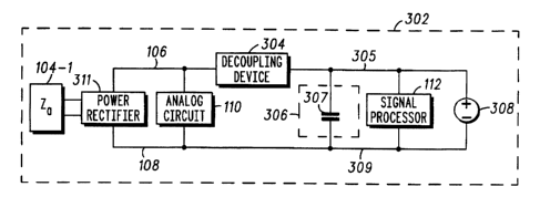
FIG. 3 shows a portable data carrier 302 that includes a decoupling
device 304 on the ingress energy path 305 to the signal processor 112.
There is further coupled to the output of the decoupling device 304 an energy
reservoir 306, disposed in parallel with the signal processor 112. In a
preferred embodiment, the energy reservoir comprises a capacitive circuit
307, as shown. Also in parallel with the signal processor 112, a voltage
regulator 308 is shown disposed between the ingress energy path 305 and
the egress energy path 309.
In a contactless embodiment as shown in FIG. 3, power is supplied
from impedance network 104-1 to analog circuit 110 and signal processor
112 through power rectifier 311. Signal processor 112 represents generically
any block that exhibits large dynamic impedance variations during normal
operation. These variations might take the form of switching noise associated
with digital circuits, discrete time analog blocks, or other analog circuits
such
as oscillators, comparators, or class-AB amplifiers. Analog circuit 110
likewise represents generically any circuit that is sensitive to voltage
fluctuations resulting from the destructive types of impedance variations
cited
above.
4
CA 02302493 2000-02-28
WO 00/00876 PCT/U599/14443
In accordance with the invention, decoupling device 304 is used to
isolate analog circuit 110 from the impedance variations of signal processor
112. As a result, the impedance seen by analog circuit 110 is determined by
decoupling device 304 and is independent of signal processor 112. To
ensure proper operation of signal processor 112, voltage regulator 308 and
capacitor 307 are used to maintain the voltage across signal processor 112
within its required operating voltage range. In particular, capacitor 307
functions as an energy reservoir and is used to supply the instantaneous
current required during each signal processor switching event, while voltage
regulator 308 is used to regulate the average voltage across signal processor
112.
Typically, decoupling device 304 is used to maintain the impedance
seen by analog circuit 110 at a substantially constant value. However, for
other applications, decoupling device 304 may be configured to allow this
impedance to vary at a rate that does not substantially degrade the
performance of analog circuit 110. For example, in a smart card application,
the impedance might be varied in a manner that is commensurate with the
rate at which the card is passed through a card reader's magnetic field. As
the card is moved closer to the reader, where the available input power is
greater, the impedance would be reduced, enabling more power to be
supplied to signal processor 112. In this way, the maximum available input
power could always be delivered to signal processor 112. In a preferred
embodiment, analog circuit 110 is a data recovery circuit and is used to
recover a data signals from an input power signal that is modulated with 10%
amplitude shift keying (ASK). According the to the invention, the impedance
of decoupling device 304 is varied at a rate that is substantially less than
the
input edge rate of the modulated data. Thus, any low frequency modulation
distortion caused by varying the impedance of device 304 can be easily
removed with a single pole high pass filter (not shown).
F1G. 4 shows a portable data device 401, including a more detailed
view of the decoupling device 304 and the voltage regulator 308. It should be
noted that the power node for this embodiment includes the contacted
terminal pads 104-2, but it is understood that such an arrangement can rely
on an impedance network 104-1, and the other analog-specific circuitry
shown in FIG. 3.
5
CA 02302493 2003-07-03
WO 00/00876 PCTNS99/14443
Decoupling device 304 is comprised of p-channel MOSFETs (metal oxide
semiconductor field effect transisto~j 403 and 404, n-channel MOSFETs 405 and
406, and
constant current source 409. N-channel MOSFETs 405 and 406 constitute a
differential pair,
which performs a current steering function, as is well known. The relative
gate voltages of
NFETs (n-field effect transistor) 405 and 406 will determine how the current
from current source
409 splits between NFETs 405 and 406. The device with the larger gate voltage
wiN have a
larger source current. PFETs (p-field effect transistor) 403 and 404 comprise
a current
mirror circuit, which, in a preferred embodiment, are sized such that the
drain
current in PFET 403 is approximately 100 times the drain current in PFET
404. The drain current for PFET 404 is substantially equal to the drain
current of NFET 406, therefore the drain current in PFET 403 will be 100
times the drain current of NFET 406. The Vref voltage applied to node 407 is
a fixed quantity. The gate voltage of NFET 406 is a fixed traction, X, of the
supply voltage Vdd applied at node 106. For X*Vdd significantly less than
Vref, none of the current from current source 400 will flow in NFET 406 and
consequently no current will flow through PFET 403. As the voltage X'Vdd is
increased, same of the current from current source 409 will flow in NFET 406
and 100 times the current in NFET 406 will flow through PFET 403. When
voltage X*Vdd equals Vref, the drain current of PFET° 403 will be 50
times the
current in current source 409 and for X*Vdd significantly greater than Vref,
all
of the current from current source 409 will flow through NFET 406 and the
current through PFET 403 will reach its maximum value of 100 times the
current source current. The differential voltage applied to the differential
pair
devices 405 and 406 controls the drain current of PFET 403. It is
substantially independent of the voltage fluctuatircns that occur due to the
activity of signal processor 912, as next shown.
Well known electronics principles suggest that the sum of the current
flowing into capacitor 30T, signal processor 192, and voltage regulator 30$
must equal the current flowing out of PFET 403. likewise, the currents
flowing out of capacitor 307, signal processor 112, and voltage regulator 308
is exactly the same as the current flowing into these elements. As a result,
the sum of the currents flowing out of capacitor 307, signal processor 112,
and voltage regulator 308 is also exactly equal to the current flowing out of
PFET 403, and therefore is independent of the activity of signal processor
112. The RC ftlter applied at the gate of PFET 403 deternnines the rate at
which the drain current of PFET 403 is varied. Accrarding to a preferred
5
CA 02302493 2003-07-03
WO 00/0087b PCT/US99/14443
embodiment of the invention, this rate is substantially less than the input
data
edge rate of the ASK modulated input power source.
Voltage regulator 308 is an active shunt regulator in the preferred
embodiment. It is comprised of an operational amplifer 413 and shunt NFET
411. The high gain characteristic of operational amplifier 413 and the
negative feedback through the resistor divider forces the minus input of
operational amplifier 413 to be equal to the Vref voltage 407. This fixes the
supply voltage for signal processor 112 to a desired level. Since voltage
regulator 308 can only sink current, it is necessary that decoupling device
304
provide mare current than required by the signal processor 112. Since the
bandwidth of operational amplifier 413 is finite, capacitor 307 is needed to
supply high frequency current required by signal processor 112 and prevent
large, high frequency fluctuations in the supply vottage for signal processor
112.
In the foregoing manner, the present invention improves receiver
sensitivity by greatly attenuating the voltage fluctuations on the received
signal that result from digital interference. Additionally, the present
invention
improves security by reducing the amount of current fluctuation from digital
switching visible over either a contacted or contactiess interface. The
beneficial properties of this invention result from the substantially constant
input impedance of the decoupling circuit. This input impedance is
independent of the signal processing element's time varying load impedance.