Note: Descriptions are shown in the official language in which they were submitted.
11093ROCA01U
CA 02302887 2000-03-29
1
LOW VOLTAGE BIPOLAR DRIVE CIRCUITS
This invention relates to drive circuits, and is
particularly concerned with drive circuits using bipolar
transistors in current mirror arrangements for operation at low
supply voltages.
Background
It is increasingly desirable to reduce the power
dissipation and increase the operating bandwidth of electronic
circuits. For these and other reasons, it may be desirable to
use bipolar transistor technology to provide a drive circuit
which operates at a low supply voltage, for example of the
order of 1.5 volts, without transistor saturation which could
decrease the operating bandwidth and increase current
consumption and hence power dissipation of the circuit. In
view of typical operating voltages of bipolar transistors,
avoiding saturation presents a considerable problem with such
low supply voltages, especially considering other factors such
as variations of the supply voltage, variations of transistor
voltages (e.g. base-emitter voltage) with temperature, and
possible cascading of circuits.
An object of this invention is to provide an improved
bipolar transistor drive circuit.
Summary of the Invention
According to one aspect of this invention there is
provided a bipolar transistor drive circuit for operation from
a low voltage supply, comprising: a first current mirror
circuit having an input and an output each coupled via a
respective resistor to a low voltage supply and constituting
respectively a signal input and a signal output of the drive
circuit; and a circuit for determining an output voltage swing
11093ROCA01U
CA 02302887 2000-03-29
2
at the signal output, said circuit comprising a voltage
reference, a compensation current mirror circuit having an
input and having an output coupled to the signal input of the
drive circuit, and a circuit for supplying to the input of the
compensation current mirror circuit a current dependent upon
the voltage reference and the supply voltage so that the signal
output voltage swing is determined substantially independently
of the supply voltage.
The circuit for supplying a current to the input of
the compensation current mirror circuit can comprise a
transistor having a base supplied with the voltage reference, a
collector coupled to the input of the compensation current
mirror circuit and via a resistor to the low voltage supply,
and an emitter coupled via a resistor to a reference potential,
for example circuit ground or 0 volts.
The drive circuit can comprise at least one further
current mirror circuit connected in cascade with the first
current mirror circuit, each further current mirror circuit
having a signal input coupled to the signal output of the
preceding current mirror circuit and an output coupled via a
resistor to the low voltage supply and constituting a signal
output of the respective current mirror circuit, and a
respective compensation current mirror circuit having an output
coupled to the signal input of the further current mirror
circuit. In this case conveniently the voltage reference and
the circuit for supplying a current to the input of the
compensation current mirror circuit can be provided commonly
for a plurality of the compensation current mirror circuits.
For handling differential signals as is often
required for a drive circuit, each of the first and any further
current mirror circuits can comprise a differential current
11093ROCAOlU
CA 02302887 2000-03-29
3
mirror circuit having differential signal inputs and outputs
each coupled via a respective resistor to the low voltage
supply, and each compensation current mirror circuit can have
two outputs coupled to the differential signal inputs of a
respective one of the first and any further current mirror
circuits.
The voltage reference can comprise a bandgap voltage
reference source and a voltage scaling circuit for reducing a
voltage provided by the bandgap voltage reference source.
The invention also provides a drive circuit
comprising: a bipolar transistor differential current mirror
having two differential current inputs and two differential
current outputs all coupled via respective resistors to a low
voltage supply, the differential inputs and outputs
constituting differential signal inputs and outputs
respectively of the drive circuit; a circuit comprising a
bipolar transistor having a base supplied with a reference
voltage, a collector coupled via a resistor to the low voltage
supply, and an emitter coupled via a resistor to a reference
potential; and a bipolar transistor current mirror having a
current input coupled to the collector of said bipolar
transistor and two current mirror outputs coupled to the
differential signal inputs, said circuit and bipolar transistor
current mirror serving to stabilize a signal voltage swing at
the differential signal outputs.
The invention further provides a drive circuit
comprising: a bipolar transistor current mirror having a
current input and a current output each coupled via a
respective resistor to a low voltage supply, the input and
output constituting a signal input and output respectively of
the drive circuit; a circuit comprising a bipolar transistor
11093ROCA01U
CA 02302887 2000-03-29
4
having a base supplied with a reference voltage, a collector
coupled via a resistor to the low voltage supply, and an
emitter coupled via a resistor to a reference potential; and a
bipolar transistor current mirror having a current input
coupled to the collector of said bipolar transistor and a
current mirror output coupled to the signal input, said circuit
and bipolar transistor current mirror serving to stabilize a
signal voltage swing at the signal output.
In addition, the invention provides a drive circuit
comprising: a first current mirror circuit comprising first
and second bipolar transistors having emitters coupled to a
reference potential, bases coupled together and to the
collector of the first transistor, and collectors of the first
and second transistors constituting a signal input and a signal
output respectively and being coupled via respective resistors
to a low voltage supply; a source of a reference voltage; a
third bipolar transistor having a base supplied with the
reference voltage, a collector coupled via a resistor to the
low voltage supply, and an emitter coupled via a resistor to a
reference potential; and a compensation current mirror circuit
comprising fourth and fifth bipolar transistors having emitters
coupled to a reference potential, bases coupled together and to
the collector of the fourth transistor, and collectors of the
fourth and fifth transistors coupled to the collectors of the
third and first transistors respectively.
Another aspect of the invention provides a method of
determining and stabilizing a signal voltage swing at an output
of a current mirror circuit, comprising the step of reducing
current at a signal input of the current mirror circuit, in
dependence upon a reference voltage and a supply voltage of the
current mirror circuit, using a compensation current mirror
11093ROCAOlU
CA 02302887 2000-03-29
circuit, so that the output signal voltage swing is not
dependent upon the supply voltage.
In this method the current mirror circuit and the
compensation current mirror circuit can comprise bipolar
5 transistors, and the supply voltage can be of the order of 1.5
volts. The method can be applied to each of a plurality of
current mirror circuits connected in cascade. In addition, the
current mirror circuits can comprise differential current
mirror circuits having differential signal inputs and outputs.
Brief Description of the Drawin s
The invention will be further understood from the
following description by way of example with reference to the
accompanying drawings, in which:
Fig. 1 schematically illustrates a known low voltage
bipolar transistor drive circuit;
Fig. 2 schematically illustrates a known bipolar
transistor current mirror circuit;
Fig. 3 schematically illustrates a known bipolar
transistor differential current mirror circuit;
Fig. 4 schematically illustrates another bipolar
transistor differential current mirror circuit;
Fig. 5 schematically illustrates a low voltage
bipolar transistor drive circuit in accordance with an
embodiment of this invention;
Fig. 6 schematically illustrates a low voltage
bipolar transistor drive circuit in accordance with another
embodiment of the invention;
11093ROCAOlU
CA 02302887 2000-03-29
6
Fig. 7 schematically illustrates a low voltage
bipolar transistor drive circuit in accordance with a further
embodiment of the invention; and
Fig. 8 schematically illustrates a bipolar transistor
voltage reference circuit which may be used in the circuit of
Fig. 5, 6, or 7.
Detailed Description
The following description omits the words "bipolar
transistor" for brevity and clarity, but it is to be understood
that the embodiments of the inventive drive circuit and the
circuits described herein relate to technologies using bipolar
transistors, as distinct for example from CMOS (complementary
metal-oxide-semiconductor) technology.
Referring to the drawings, Fig. 1 illustrates a known
low voltage drive circuit for a differential signal, comprising
a differential amplifier including NPN transistors 10 and 12 in
a long-tailed pair configuration, with their collectors
connected via respective resistors 11 and 13 to a positive
supply voltage Vp, and with their emitters connected together
and via the collector-emitter path of an NPN transistor 14 and
a resistor 15 to ground (0 volts, abbreviated to OV). A bias
voltage Vb is supplied to the base of the transistor 14, a
differential binary input signal is supplied to the bases of
the transistors 10 and 12, and a differential digital output
signal is derived from the collectors of the transistors 10 and
12. For example, with a nominal supply voltage of 1.5 volts,
each output connection may be desired to change between
substantially this voltage Vp=1.5V and a lower voltage of 1
volt, i.e. to have an output voltage swing of 0.5V.
11093ROCAOlU
CA 02302887 2000-03-29
7
Typically in such a circuit the bias voltage Vb is
selected for a desired base-emitter voltage (Vbe) of the
transistor 14 plus a desired voltage drop across the resistor
15, whose resistance R15 (for convenience and clarity,
throughout this description the resistance of a resistor is
represented by the letter R followed by the drawing reference
numeral of the resistor) is selected to provided a desired low
current for the differential transistors 10 and 12. The
desired voltage drop across the resistor 15 may for example be
0.15V.
A significant problem with such a circuit is that the
supply voltage Vp may vary, for example by ~10% so that it can
be as low as 1.35V, and the transistor Vbe can vary for example
between 0.75V and 0.9V, so that under worst case conditions of
minimum supply voltage and maximum Vbe there is a very low
voltage for biasing the transistor 14. Consequently, this
leads to operation at levels very close to transistor
saturation, which is undesirable for high frequency and low
current operation, and makes the circuit susceptible to noise.
Operation of such a circuit at an even lower supply voltage,
for example with a supply voltage of 1.3V as may be desired, is
substantially impractical.
Accordingly, it is desirable to provide a different
form of drive circuit, for which reason embodiments of the
invention as described below make use of current mirror (CM)
circuits. One known CM circuit is illustrated in Fig. 2.
Referring to Fig. 2, two NPN transistors 20 and 22
have their bases connected together and their emitters
connected via respective resistors 21 and 23 to ground (OV).
The transistor 20 is diode-connected by a connection between
its collector and base. An input current iin supplied to the
11093ROCAOlU
CA 02302887 2000-03-29
8
interconnected collector and base of the transistor 20 is
mirrored by the transistor 22 to produce in its collector
circuit an output current iout, with a gain m which is
determined by area ratios of the transistors 20 and 22 and
resistances of the resistors 21 and 23. The collectors of the
transistors can be connected via respective resistors (not
shown in Fig. 2) to a positive supply voltage (not shown in
Fig. 2). As is known in the art, the emitter resistors 21 and
23 can optionally be omitted.
The CM circuit of Fig. 2 is single-ended, and can be
substantially duplicated to provide a known differential
current mirror (DCM) circuit as shown in Fig. 3. Thus the DCM
circuit of Fig. 3 comprises NPN transistors 30, 32, 34, and 36
and respective emitter resistors 31, 33, 35, and 37 connected
to ground (OV); the resistors can optionally be omitted. The
transistors 30 and 34 are each diode-connected and have their
bases connected to the bases of the transistors 32 and 36
respectively, so that differential input currents i+in and i-in
supplied to the transistors 30 and 34 are mirrored to produce
differential output currents i+out and i-o"t in the collector
circuits of the transistors 32 and 36 respectively. The DCM
circuit can provide a gain m so that nominally the equation
(1+out-1-out)=m(i+in-i-in) 1S SatlSfied.
It is desirable that this equation be met precisely,
i.e. that there be no differential current offset, but
typically with the DCM circuit of Fig. 3 there is also a
differential current offset so that this equation is not
precisely met. Another DCM circuit, in which the differential
current offset is reduced or eliminated, is illustrated in Fig.
4.
11093ROCAOlU
CA 02302887 2000-03-29
9
Referring to Fig. 4, the DCM circuit illustrated
therein comprises NPN transistors 40, 42, 44, and 46, the
transistors 40 and 44 each being diode-connected with their
bases connected to the bases of the transistors 42 and 46
respectively, differential input currents i+in and i-in supplied
to the transistors 40 and 44 being mirrored to produce
differential output currents i+out and i-out in the collector
circuits of the transistors 42 and 46 respectively. The DCM
circuit of Fig. 4 differs from that of Fig. 3 in that the
emitters of the input transistors 40 and 44 are connected
together and via a resistor 41 to ground (OV), and the emitters
of the output transistors 42 and 46 are connected together and
via a resistor 43 to ground (OV). The resistors 41 and 43 can
alternatively be replaced by constant current circuits. As
indicated above, the DCM circuit of Fig. 4 more precisely
satisfies the equation (i+out-i-out)=m(i+in-i-i"), where m is the
current mirror gain.
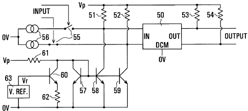
Fig. 5 illustrates a low voltage drive circuit, in
accordance with an embodiment of this invention, which includes
a DCM circuit 50 which can have the form of Fig. 3 but
preferably has the form of Fig. 4. As illustrated in Fig. 5,
the DCM circuit 50 has a two-wire input IN for the differential
input currents i+i" and i-in, these two wires being connected via
respective resistors 51 and 52 to a positive supply voltage Vp.
The DCM circuit 50 also has a two-wire output OUT for the
output currents i+out and i-out. these two wires being connected
via respective resistors 53 and 54 to the positive supply
voltage Vp. For example Vp=1.5 volts. The DCM circuit 50
provides a current gain m between its input and its output; for
low power operation with very high frequency digital signals,
up to about 5 GHz, for example m may be of the order of 4 to
10. The resistances of the resistors 51 and 52 are equal, i.e.
11093ROCAOlU
CA 02302887 2000-03-29
R51=R52, and the resistances of the resistors 53 and 54 are
equal, i.e. R53=R54.
The two-wire input IN of the DCM circuit 50 is
supplied with a differential input signal which for
5 illustrative purposes is shown in Fig. 5 as being provided by a
circuit comprising two switches 55, controlled in a
complementary manner from a differential input, each for
coupling a respective one of two current sources 56 to a
respective one of the resistors 51 and 52 to supply a current
10 thereto when the switch is closed. Any other desired form of
input circuit can instead be provided for supplying currents
differentially to the resistors 51 and 52, and the particular
circuit illustrated is given only by way of example.
Furthermore, in a cascade arrangement of several DCM circuits
as further described below the output of one DCM circuit can
directly constitute the input for the next DCM circuit in the
cascade. Thus there can be only one DCM circuit or, especially
when DCM circuits of the form illustrated in Fig. 4 are used,
there can be several series-connected DCM circuits. The two-
wire output of the DCM circuit 50, providing the differential
output currents i+out and i-o"t which flow via the resistors 53
and 54 respectively, constitute a differential output of the
drive circuit of Fig. 5.
The drive circuit of Fig. 5 also includes a
compensation circuit comprising four NPN transistors 57 to 60,
two resistors 61 and 62, and a voltage reference source 63
which provides a reference voltage Vr to the base of the
transistor 60. The transistor 60 has its collector coupled via
the resistor 61 to the positive supply voltage Vp and its
emitter coupled to ground (OV) via the resistor 62. The
collector of the transistor 60 is also connected to the
11093ROCAOlU
CA 02302887 2000-03-29
11
collector and base of the transistor 57 which is thereby diode-
connected, and to the bases of the transistors 58 and 59. The
emitters of the transistors 57 to 59 are connected to ground
(OV), so that these transistors constitute a current mirror
with a gain m~ from the transistor 57 to each of the transistors
58 and 59. The collectors of the transistors 58 and 59 are
connected respectively to the resistors 51 and 52, and hence to
the two-wire input IN of the DCM circuit 50. Emitter
resistors, not shown, may optionally be included between the
emitters of the transistors 57 to 59 and ground (OV).
In operation of the drive circuit of Fig. 5, the
complementary switches 55 are controlled by the input signal so
that the resistors 51 and 52 conduct current alternately,
whereby the input transistors 40 and 44 (Fig. 4, or 30 and 34,
Fig. 3) of the DCM circuit 50 also conduct alternately, their
currents being mirrored with the gain m by the output
transistors 42 and 46 (Fig. 4, or 32 and 36, Fig. 3). The
output transistor currents flow via the resistors 53 and 54 to
provide across these resistors an output voltage swing having a
desired amplitude, for example 0.5V as described above.
The compensation circuit serves to determine and
stabilize this output voltage swing in the manner described
below. In the following description, it is assumed for
simplicity that the DCM circuit 50 has the form of Fig. 4 with
the resistors 41 and 43 having zero resistance or being
omitted; this is the same as the form of Fig. 3 with its
emitter resistors omitted. A similar result can be derived in
either case when the respective resistors are present.
Although the following description relates to only one half of
the DCM circuit 50 and the corresponding resistors and parts of
11093ROCAOlU
CA 02302887 2000-03-29
12
the compensation circuit, it can be appreciated that the same
comments apply for the other half.
The reference voltage Vr supplied by the source 63 is
selected to be equal to a reference voltage Vref plus one Vbe,
i.e. the base-emitter voltage of one transistor. The reference
voltage Vref is desirably derived from a precise temperature-
stable bandgap voltage reference as described later below.
Consequently, the emitter voltage of the transistor 60 is equal
to Vref, and this transistor 60 conducts a current i6o equal to
Vref/R62, where as indicated above R62 is the resistance of the
resistor 62. The resistor 61 drops a voltage equal to Vp-Vbes~
where Vbes~ is the base-emitter voltage of the transistor 57.
Consequently, the transistor 57 conducts a current i5~ given by:
i5~ _ ( Vp-VbeS~ ) /R61 - Vref /R62 .
This current is mirrored by the transistor 58 with
the gain m~ to produce a proportional current i58=m~is~ conducted
by the transistor 58. With the states of the switches 55 as
shown in Fig. 5, the resistor 51 drops a voltage Vp-Vbein where
Vbein is the base-emitter voltage of the input transistor 40 of
the DCM circuit 50, and this transistor 40 consequently
conducts a current iin given by:
lin = (Vp-Vbein) /R51 - m~i5~.
This current is mirrored by the transistor 42 with
the gain m to produce a proportional output current lout=main
which flows via the resistor 53, producing a voltage drop VR9
equal to mR53iin which constitutes the output voltage swing of
the drive circuit. Combining these equations gives:
= m(R53/R51) {Vp-Vbei"-m~(R51/R61) (Vp-VbeS~-(R61/R62)Vref) },
from which it can be seen that if the values m~, R51, and R61
are selected so that m~(R51/R61)=1, and if Vbe;,n=VbeS~, then:
VR9 = m (R53/R51) (R61/R62 ) Vref .
11093ROCAOlU
CA 02302887 2000-03-29
13
Thus it can be seen that the output voltage swing is
dependent only upon the gain m of the DCM circuit 50,
resistance ratios of the resistors 51, 53, 61, and 62, all of
which are fixed and predetermined, and the reference voltage
Vref which is also fixed, predetermined, and temperature-
stable. Consequently, the output voltage swing is stable, as
is desired.
As indicated above, the DCM circuit 50 in the drive
circuit of Fig. 5 may provide only a relatively small current
gain m, whereas a considerably larger current gain may be
desired. Such a larger current gain can be provided by
connecting two or more similar drive circuit stages in cascade,
as illustrated in Fig. 6 and as described below. In such a
cascade of drive circuits, some or all of the components 57 and
60-63 of the circuit of Fig. 5 can be used commonly for a
plurality of stages, and between successive stages a single
pair of resistors can constitute both the output resistors (53
and 54 as shown in Fig. 4) of the preceding DCM circuit and the
input resistors (51 and 52 in Fig. 4) of the following DCM
circuit.
Fig. 6 illustrates a drive circuit comprising a
cascade of two current gain stages, a first one of which is the
same as described above with reference to Fig. 5 and uses the
same reference numerals. The drive circuit of Fig. 6 further
comprises a DCM circuit 64, resistors 65 and 66, and NPN
transistors 68 and 69. The DCM circuit 64 has a two-wire input
IN which is connected to the two-wire output OUT of the DCM
circuit 50 and hence also to the resistors 53 and 54, and a
two-wire output OUT for its output currents, these two wires
being connected via the respective resistors 65 and 66 to the
positive supply voltage Vp, and constituting a differential
11093ROCAOlU
CA 02302887 2000-03-29
14
output of the drive circuit. The transistors 68 and 69 have
their collectors connected respectively to the two wires of the
input of the DCM circuit 64, their emitters connected to ground
(OV), and their bases connected to the base of the transistor
57 to form a second current mirror pair with that transistor.
Emitter resistors, not shown, may optionally be included
between the emitters of the transistors 57 to 59, 68, and 69
and ground (OV).
Thus the arrangement of the input-side resistors 53
and 54, current mirror transistors 68 and 69, and output-side
resistors 65 and 66 with respect to the DCM circuit 64 is the
same as the arrangement of the input-side resistors 51 and 52,
current mirror transistors 58 and 59, and output-side resistors
53 and 54 respectively with respect to the DCM circuit 50. The
current mirror comprising the transistors 57, 68, and 69 can
provide a respective gain mil to provide compensation for the
DCM circuit 64 in the same manner as described above by
selecting values so that m~l(R53/R61)=1, and if the DCM circuit
64 provides a gain ml then its output voltage swing, equal to
ml(R65/R53)(R61/R62)Vref, is also stable. The overall gain of
the cascaded drive circuit of Fig. 6 is the product of the
gains m and ml of the DCM circuits 50 and 64 respectively.
It can be appreciated that such cascading can be
applied to a larger number of stages in a similar manner. It
can also be appreciated that alternatively different reference
voltage sources and current mirror compensation circuits can be
provided for different ones of the stages. The same comments
apply to single-ended current mirror stages as further
described below.
Although the drive circuits of Figs. 5 and 6 use
differential current mirrors for handling differential signals,
11093ROCAOlU
CA 02302887 2000-03-29
the invention is equally applicable to single-ended drive
circuits, an example of which is illustrated in Fig. 7. The
drive circuit of Fig. 7 is similar to that of Fig. 5 and
accordingly uses the same reference numerals where applicable,
5 except that it is arranged for a single-ended signal and
accordingly one of the switches 55 and current sources 56 of
the example input circuit are omitted, the compensation circuit
transistor 59 and the resistors 52 and 54 are omitted, and the
DCM circuit 50 of Fig. 5 is replaced by a CM circuit of the
10 form shown in Fig. 2, comprising the transistors 20 and 22, in
this case the resistors 21 and 23 also being omitted. The
operation of the drive circuit of Fig. 7, and the manner in
which a stable output voltage swing is provided, is
substantially the same as described above with reference to
15 Fig. 5, and it will be appreciated that such a single-ended
arrangement can also use a cascade of CM circuits in a similar
manner to that described above with reference to Fig. 6.
Fig. 8 illustrates one form of circuit which may be
used to constitute the voltage reference source 63. The
circuit comprises a voltage source circuit 78 and a voltage
scaling circuit 79.
The voltage source circuit 78 comprises NPN
transistors 80 to 83, resistors 84 to 86, and a current source
87. The transistor 80 has its emitter connected to ground
(OV), and its collector connected to its base and via the
resistor 84 to a line 88 on which the circuit produces a
temperature-stable so-called bandgap reference voltage Vbg.
The transistor 81 has its emitter connected via the resistor 85
to ground (OV), and its base connected to the base of the
transistor 80, the transistor 81 being sized relative to the
transistor 80 to provide different current densities through
11093ROCAOlU
CA 02302887 2000-03-29
16
the transistors 80 and 81. The collector of the transistor 81
is connected via the resistor 86 to the line 88. The
transistor 82 has its base connected to the collector of the
transistor 81, its emitter connected to ground (OV), and its
collector connected via the current source 87 to a positive
voltage +V which typically may be higher than the voltage Vp.
The transistor 83 has its collector connected to the voltage
+V, its emitter connected to the line 88, and its base
connected to the collector of the transistor 82. A voltage
reference output line 89 of the circuit 78 is also connected to
the collector of the transistor 82, providing a reference
voltage equal to the voltage Vbg on the line 88 plus the base-
emitter voltage Vbe of the transistor 83.
As the voltage on the line 89 is typically higher
than is desired for the voltage Vr required for operation of
the drive circuit as described above with its low supply
voltage Vp, this voltage on the line 89 is scaled by the
scaling circuit 79. The circuit 79 comprises NPN transistors
90 and 91, a differential amplifier 92, and resistors 93 to 96.
The transistor 90 has its base connected to the line 89, its
emitter connected via the resistor 94 to ground (OV), and its
collector connected via the resistor 93 to the voltage +V. The
transistor 91 has its emitter connected via the resistor 96 to
ground (OV) and its collector connected via the resistor 95 to
the voltage +V. The differential amplifier 92 has a non-
inverting input (+) connected to the collector of the
transistor 90, an inverting input (-) connected to the
collector of the transistor 91, and an output connected to the
base of the transistor 91 and to an output line 98 providing
the reference voltage Vr.
11093ROCA01U
CA 02302887 2000-03-29
17
It can be appreciated from the above description and
the circuit of Fig. 8 that the emitter of the transistor 90 is
at the voltage Vbg, and that the differential amplifier 92
maintains the circuit so that the emitter of the transistor 91
is at a proportional voltage kVbg, where k is a scaling
constant (typically less than one) equal to (R96/R95)(R93/R94),
where R93 to R96 are the resistances of the resistors 93 to 96
respectively. The output voltage of the differential amplifier
92 is at this scaled voltage kVbg plus the base-emitter voltage
Vbe of the transistor 91, this constituting the desired
reference voltage Vr.
It can be appreciated that the desired reference
voltage Vr can be produced in any other desired manner.
The drive circuits described above provide advantages
in that they operate at a low supply voltage and with a low
power in an efficient manner to provide outputs with stable and
predetermined voltage swings, thereby avoiding transistor
saturation especially when several of the drive circuits are
connected in cascade. Consequently, the drive circuits can
operate with very high signal frequencies, for example up to
about 5 GHz.
Although particular embodiments of the invention have
been described above, it can be appreciated that numerous
modifications, variations, and adaptations may be made without
departing from the scope of the invention as defined in the
claims.