Note: Descriptions are shown in the official language in which they were submitted.
CA 02302899 2000-03-29
- 1 -
TITLE OF THE INVENTION
OPTICAL WIRING LAYER, OPTOELECTRIC WIRING SUBSTRATE,
MOUNTED SUBSTRATE, AND METHODS FOR MANUFACTURING THE
SAME
BACKGROUND OF THE INVENTION
The present invention relates to an optical wiring
layer through which light propagates, an optoelectric
wiring substrate comprising the optical wiring layer
and a substrate having an electric wiring, a mounted
substrate in which an optical part or the like is
mounted on the optoelectric wiring substrate, and
methods for manufacturing each of these structures.
In the field of electric elements such as
semiconductor large-scale integrated circuits (LSI),
the degree of integration of transistors has been
increasing. Some semiconductor large-scale integrated
circuits Among these LSIs are those which operate at
so high a clock frequency as 1 GHz.
To mount highly integrated electric elements on an
electric wiring substrate, packages such as BGAs (Ball
Grid Arrays) and CSPs (Chip Size Packages) have been
developed and put to practical use.
In general, the inter-element signal speed outside
an electric element increases linearly with the clock
frequency inside the electric element. The increase in
inter-element signal speed induces noise such as
reflection arising from the inappropriate shape of an
CA 02302899 2000-03-29
- 2 -
electric wiring joining elements together, or cross
talk. Another problem may occur that this increase
causes an increased amount of electromagnetic waves to
be generated from the electric wiring to adversely
affect the surroundings. Thus, in constructing
systems, the signal speed between electric elements is
diminished enough to prevent these problems. As a
result, highly integrated electric elements cannot
fully provide their functions.
In order to solve these problems, the following
methods have been contemplated: Part of an electric
wiring on an electric wiring substrate is replaced with
an optical wiring comprised of optical fibers so that
optical signals are used instead of electric signals.
This is because optical signals do not cause noise or
electromagnetic waves.
An example of this method if disclosed in Japanese
Laid-Open Patent Publication (Kokai) No. 9-236731.
This is a method for forming optical waveguides on an
electric wiring substrate. Specifically, optical
waveguides are directly formed on a ceramic multilayer
wiring substrate (in the order of a clad layer, a core
pattern, and a clad layer).
Multiple layers of electric wirings, however, are
formed on a surface of the electric wiring substrate,
which acts as an under layer of the optical wiring
layer. This electric wiring forms very large recesses
CA 02302899 2007-11-30
29015-7
- 3 -
and projections. Thus, disadvantageously, when the optical
waveguides are formed on the electric wiring substrate, the
propagation loss of optical waves increases.
BRIEF SUMMARY OF THE INVENTION
The present invention is provided in view of these
circumstances, and it is an object thereof to provide an
optical wiring layer, an optoelectric wiring substrate, a
mounted substrate, and methods for manufacturing these
structures wherein the propagation loss of optical signals
is small and wherein high-density mounting and size
reduction can be achieved.
One aspect of the present invention is an
optoelectric substrate comprising a substrate having an
electric wiring and an optical wiring layer prepared in
advance and laminated on the substrate via an adhesive which
coats the electric wiring and absorbs recesses of the
electric wiring, said optical wiring layer comprising: a
core through which light propagates; a clad for holding
optical signals within said core; a mirror for reflecting
light propagating through said core; first conductive
installation means formed on a surface of said optical
wiring layer for installing light-receiving means for
receiving light reflected by said mirror or light-emitting
means for emitting light toward said mirror; and connection
means for electrically connecting said first conductive
installation means to said electric wiring.
According to this optoelectric wiring substrate,
an optical wiring layer is laminated on a substrate having
CA 02302899 2007-11-30
29015-7
- 4 -
an electric wiring, in addition, conductive installation
means, which install an optical part on the optical wiring
layer, are provided. The optical part installed on the
conductive installation means is electrically connected to
the electric wiring.
Accordingly, with this configuration, the optical
wiring layer is laminated on the substrate with the electric
wiring. As a result, high-density mounting and size
reduction can be achieved.
Another optoelectric wiring substrates according
to present invention are as follows:
(1) Another aspect of the present invention is an
optoelectric substrate comprising a substrate having an
electric wiring and an optical wiring layer prepared in
advance and laminated on the substrate via an adhesive which
coats the electric wiring and absorbs recesses of the
electric wiring, said optical wiring layer comprising: a
core through which light propagates; a clad for holding
optical signals within said core; a mirror for reflecting
light propagating through said core; conductive installation
means formed on a surface of said optical wiring layer for
installing an electric part; and connection means for
electrically connecting said second conductive installation
means to said electric wiring.
According to this optoelectric wiring substrate,
an optical wiring layer is laminated on a substrate having
an electric wiring, in addition, conductive installation
means, which install an electric part on the optical wiring
layer, are provided. The electric part installed on the
CA 02302899 2007-11-30
29015-7
- 5 -
conductive installation means is electrically connected to
the electric wiring.
Accordingly, with this configuration, high-density
mounting and size reduction can be achieved.
(2) Another aspect of the present invention is an
optoelectric substrate comprising a substrate having an
electric wiring and an optical wiring layer prepared in
advance and laminated on the substrate via an adhesive which
coats the electric wiring and absorbs recesses of the
electric wiring, said optical wiring layer comprising: a
core through which light propagates; a clad for holding
optical signals within said core; a mirror for reflecting
light propagating through said core; first conductive
installation means formed on a surface of said optical
wiring layer for installing light-receiving means for
receiving light reflected by said mirror or light-emitting
means for emitting light toward said mirror; second
conductive installation means formed on said optical wiring
layer surface for installing an electric part; connection
means for each of said conductive installation means to said
electric wiring.
According to this optoelectric wiring substrate,
an optical wiring layer is laminated on a substrate having
an electric wiring, in addition, first conductive
installation means for installing an optical part and second
conductive installation means for installing an electric
part, are provided. The optical part and the electric part
installed on each of the conductive installation means are
electrically connected to the electric wiring.
CA 02302899 2007-11-30
29015-7
- 6 -
Accordingly, with this configuration, high-density
mounting and size reduction can be achieved.
(3) Another aspect of the present invention is an
optoelectric substrate comprising a substrate having an
electric wiring and an optical wiring layer prepared in
advance and laminated on the substrate via an adhesive which
coats the electric wiring and absorbs recesses of the
electric wiring, said optical wiring layer comprising a
first clad; a first core formed on said first clad through
which light propagates; a mirror for reflecting light
propagating through said first core; a second core formed on
said first clad using a material identical to that of said
first core; first conductive installation means laminated on
said second core for installing light-receiving means for
receiving light reflected by said mirror or light-emitting
means for emitting light toward said mirror; connection
means for electrically connecting said first conductive
installation means to said electric wiring, and a second
clad for covering at least one of said first clad, said
first core, said mirror, said second core, and said
connection means.
According to this optoelectric wiring substrate,
an optical wiring layer is laminated on a substrate having
an electric wiring, in addition, conductive installation
means, which install an optical part on the optical wiring
layer, are provided. The optical part installed on the
conductive installation means is electrically connected to
the electric wiring.
CA 02302899 2007-11-30
29015-7
- 7 -
Accordingly, with this configuration, high-density
mounting and size reduction can be achieved.
(4) Another aspect of the present invention is an
optoelectric substrate comprising an optical wiring layer
prepared in advance and laminated on a substrate having an
electric wiring via an adhesive which coats the electric
wiring and absorbs recesses of the electric wiring, said
optical wiring layer comprising a first clad; a first core
formed on said first clad through which light propagates; a
mirror for reflecting light propagating through said first
core; a second core formed on said first clad using a
material identical to that of said first core; conductive
installation means laminated on said second core for
installing an electric part; connection means for
electrically connecting said second conductive installation
means to said electric wiring, and a second clad for
covering at least one of said first clad, said first core,
said mirror, said second core, and said connection means.
According to this optoelectric wiring substrate,
an optical wiring layer is laminated on a substrate having
an electric wiring, in addition, conductive installation
means, which install an electric part on the optical wiring
layer, are provided. The electric part installed on the
conductive installation means is electrically connected to
the electric wiring.
Accordingly, with this configuration, high-density
mounting and size reduction can be achieved.
(5) Another aspect of the present invention is an
optoelectric substrate comprising an optical wiring layer
prepared in advance and laminated on a substrate having an
electric wiring via an adhesive which coats the electric
wiring and absorbs recesses of the electric wiring, said
CA 02302899 2007-11-30
29015-7
- 8 -
optical wiring layer comprising a first clad; a first core
formed on said first clad through which light propagates; a
mirror for reflecting light propagating through said first
core; a second core formed on said first clad using a
material identical to that of said first core; first
conductive installation means formed on said second core for
installing light-receiving means for receiving light
reflected by said mirror or light-emitting means for
emitting light toward said mirror; second conductive
installation means formed on said second core for installing
an electric part; connection means for electrically
connecting said each of said connection means to said
electric wiring, and a second clad for covering at least one
of said first clad, said first core, said mirror, said
second core, and said connection means.
According to this optoelectric wiring substrate,
an optical wiring layer is laminated on a substrate having
an electric wiring, in addition, first conductive
installation means for installing an optical part and second
conductive installation means for installing an electric
part, are provided. The optical part and the electric part
installed on each of the conductive installation means are
electrically connected to the electric wiring.
CA 02302899 2000-03-29
- 9 -
Accordingly, with this configuration, high-density
mounting and size reduction can be achieved.
(6) The present invention is an optoelectric
wiring substrate comprising: a substrate having an
electric wiring; a first optical wiring layer laminated
on one of the surfaces of the substrate and having a
core through which light propagates and a clad for
holding the core; a second optical wiring layer
laminated on the other surface of the substrate and
having a core through which light propagates and a clad
for holding the core; a third optical wiring layer
penetrating the substrate in a perpendicular direction
and having a core through which light propagates and a
clad for holding the core; a first mirror formed to
extend through the first optical wiring layer and the
third optical wiring layer for reflecting light;
propagating through one of the optical wiring layers,
to the other optical wiring layer; and a second mirror
formed to extend through the second optical wiring
layer and the third optical wiring layer for reflecting
light propagating through one of the optical wiring
layers, to the other optical wiring layer.
According to this optoelectric wiring substrate,
the third optical wiring layer penetrating the
substrate in a perpendicular direction is connected the
first optical wiring layer laminated on one of the
surfaces of the substrate and the second optical wiring
CA 02302899 2000-03-29
- 10 -
layer laminated on the other surface. In each of
connection areas between the cores, a mirror for
reflecting light propagating through one of the optical
wiring layers to the other optical wiring layer is
provided.
Accordingly, with this configuration, light is
reflected by the mirror and propagates the third
optical wiring layer so that light can propagate from
one of the surfaces to the other surface.
Incidentally, it is preferable that each of the
optoelectric wiring substrates further comprises
alignment means formed a material to that of the core
for using alignment with the substrate having the
electric wiring.
Furthermore, it is preferable that each of the
optoelectric wiring substrate further comprises
alignment means formed a material to that of the first
core for using alignment on forming of the mirror.
The above construction can implement an optical
wiring layer, an optoelectric wiring substrate, a
mounted substrate, and methods for manufacturing these
structures wherein the propagation loss of optical
signals is small and wherein high-density mounting and
size reduction can be achieved.
In addition, the present invention is an optical
wiring layer comprising: a first optical wiring layer
having a core through which light propagates and a clad
CA 02302899 2000-03-29
- 11 -
for holding the core; a second optical wiring layer
having a core through which light propagates and a clad
for holding the core, the second optical wiring layer
being connected to the first optical wiring layer at a
predetermined angle; and a mirror formed to extend
through the first optical wiring layer and the second
optical wiring layer for reflecting light propagating
through one of the cores, to the other core.
According to this optical wiring layer, the second
optical layer is connected to the first optical layer
at a predetermined angle. In connection area between
the cores, a mirror, which reflects light propagating
through one of the cores, to the other core, is formed.
Furthermore, it is possible that the present
invention is an optoelectric wiring substrate
comprising: the optical wiring layer according to claim
14; and a substrate having an electric wiring on which
the optical wiring layer is laminated.
Accordingly, with this configuration, high-density
mounting and size reduction can be achieved.
Furthermore, it is possible that the present
invention is a mounted substrate comprising : the
optical wiring substrate and an optical part installed
on the first conductive installation means for
receiving light reflected by the mirror or emitting
light toward the mirror.
Accordingly, with this configuration, high-density
CA 02302899 2006-10-02
29015-7
- 12 -
mounting and size reduction can be achieved.
Furthermore, it is possible that the present
invention is a mounted substrate comprising: the optical
wiring substrate; and an electric part installed on the
second conductive installation means for receiving light
reflected by the mirror or emitting light toward the mirror.
Accordingly, with this configuration, high-density
mounting and size reduction can be achieved.
The above construction can implement an optical
wiring layer, an optoelectric wiring substrate, a mounted
substrate, and methods for manufacturing these structures
wherein the propagation loss of optical signals is small and
wherein high-density mounting and size reduction can be
achieved.
Another aspect of the present invention is a
method for manufacturing an optoelectric wiring substrate,
comprising the steps of: forming an optical wiring layer on
a smooth first support substrate; forming a mirror for
reflecting light propagating through the optical wiring
layer; releasing the optical wiring layer from the smooth
first support substrate and sticking the optical wiring
layer on a substrate having an electric wiring via an
adhesive; and forming conductive installation means on the
optical wiring layer for installing an optical or electric
part to be mounted on the optoelectric wiring substrate, the
conductive
CA 02302899 2007-11-30
29015-7
- 13 -
installation means being electrically connected to the
electric wiring.
According to this method for manufacturing an
optoelectric wiring substrate, after being manufactured on
the flat first support substrate, the optical wiring layer
is stuck to the substrate with the electric wiring. Thus,
the effect of recesses and projections of the electric
wiring on the substrate can be lessened compared to an
optical wiring layer directly manufactured on the substrate
with an electric wiring.
Another optoelectric wiring substrates according
to present invention are as follows:
(1) According to another aspect the present
invention is a method for manufacturing an optoelectric
wiring substrate, comprising the steps of: forming an
optical wiring layer on a smooth first support substrate;
forming a mirror for reflecting light propagating through
the optical wiring layer; releasing said optical wiring
layer from said smooth first support substrate, and sticking
one of surface of said optical wiring layer on a smooth
second support substrate using a first adhtesive; applying a
second adhesive to said substrate having an electric wiring;
sticking the other surface of said optical wiring layer on
said second adhesive; and releasing said smooth second
support substrate and said first adhesive from said optical
wiring layer.
According to this method for manufacturing an
optoelectric wiring substrate, the optical wiring layer
CA 02302899 2007-11-30
29015-7
- 14 -
is fixed to the smooth second support substrate so as to be
stuck to the electric wiring substrate while maintaining its
smoothness.
With this configuration, the optical wiring layer
of the optoelectric wiring substrate is not affected by the
unevenness of the underlying electric wiring substrate
surface. The propagation loss of optical signals can be
minimized.
(2) According to another aspect the present
invention is a method for manufacturing an optoelectric
wiring substrate, comprising the steps of: forming an
optical wiring layer on a smooth second support substrate;
forming a mirror for reflecting light propagating through
the optical wiring layer; applying an adhesive to a
substrate having an electric wiring; sticking said optical
wiring layer on said adhesive; and releasing said smooth
second support substrate from said optical wiring layer.
According to this method for manufacturing an
optoelectric wiring substrate, the optical wiring layer is
fixed to the smooth second support substrate so as to be
stuck to the electric wiring substrate while maintaining its
smoothness.
With this configuration, the optical wiring layer
of the optoelectric wiring substrate is not affected by the
unevenness of the underlying electric wiring substrate
surface. The propagation loss of optical signals can be
minimized.
(3) the present invention is a method for
CA 02302899 2000-03-29
- 15 -
manufacturing an optoelectric wiring substrate
comprising the step of: forming a first through-hole in
a substrate having an electric wiring; forming first
clads on both surfaces of the substrate and filling a
clad in the first through-hole; forming a second
through-hole in the first through-hole which has a
smaller inner diameter than the first through-hole;
covering the clad with a core layer to fill the second
through-hole with a core, in order to obtain an optical
wiring extending along the substrate and an optical
wiring penetrating the optical wiring; removing
portions of the core layer which are not used as the
optical wirings, in order to expose the first clad;
forming a second clad on exposed portions of the first
clad and core layer, the second clad having a
refractive index equal to that of the first clad; and
forming a mirror for reflecting light from the optical
wiring extending along the substrate to the optical
wiring penetrating the optical wiring.
In addition, the present invention is a method for
manufacturing an optoelectric wiring substrate
comprising the step of: forming a release film on a
smooth support substrate; forming a first optical
wiring layer on the release layer which comprises a
first core through which light propagates in a first
direction and a clad for holding the first core;
forming a hole in the first optical wiring layer which
CA 02302899 2000-03-29
- 16 -
is inclined at a predetermined angle relative to the
first optical wiring layer; filling a core in the hole
to form a second core through which light propagates in
a second direction; forming a mirror such that light
from the first core is incident on the second core for
reflecting light propagating through one of the optical
wiring layers, to the other optical wiring layer; and
releasing the optical wiring layers from the smooth
support substrate.
The optoelectric wiring substrates according to
each of the method of manufacturing can guide light
from one surface of the substrate having the electric
wiring to the other surface.
The above construction can implement an optical
wiring layer, an optoelectric wiring substrate, a
mounted substrate, and methods for manufacturing these
structures wherein the propagation loss of optical
signals is small and wherein high-density mounting and
size reduction can be achieved.
Additional objects and advantages of the invention
will be set forth in the description which follows, and
in part will be obvious from the description, or may be
learned by practice of the invention. The objects and
advantages of the invention may be realized and
obtained by means of the instrumentalities and
combinations particularly pointed out hereinafter.
CA 02302899 2000-03-29
- 17 -
BRIEF DESCRIPTION OF THE SEVERAL VIEWS OF THE DRAWING
The accompanying drawings, which are incorporated
in and constitute a part of the specification,
illustrate presently preferred embodiments of the
invention, and together with the general description
given above and the detailed description of the
preferred embodiments given below, serve to explain the
principles of the invention.
FIG. 1 is a top view of an optoelectric wiring
substrate according to a first embodiment as seen from
an optical part-mounted side.
FIG. 2A is a sectional view taken along the
direction C-C in FIG. 1.
FIG. 2B shows another example of an optoelectric
wiring substrate according to the first embodiment.
FIGS. 3A and 3B show an optoelectric wiring
substrate in which only part of pads 509 for electric
connections with an optical part are exposed.
FIG. 4 is a top view of an optoelectric wiring
substrate with no alignment mark formed therein as seen
from the optical part-mounted side.
FIGS. 5A to 50 show each step of a method for
manufacturing an optoelectric wiring substrate 50.
FIGS. 6A to 6M show each step of another method
for manufacturing the optoelectric wiring substrate 50.
FIGS. 7A to 7P show each step of another method
for manufacturing an optoelectric wiring substrate 53.
CA 02302899 2000-03-29
- 18 -
FIGS. 8A and 8B show the steps of manufacturing a
resin layer 58.
FIG. 9A shows a mounted substrate 60 in which a
light-emitting element 58 is mounted on an optoelectric
wiring substrate 55.
FIG. 9B shows a mounted substrate 62 in which the
light-receiving element 59 is mounted on the
optoelectric wiring substrate 55.
FIG. 10 is a mounted substrate 62 in which a BGA
package 66 that is an electric part is mounted on an
optoelectric wiring substrate.
FIGS. 11A to 11N show each step of a method for
manufacturing an optoelectric wiring substrate
according to a second embodiment.
FIGS. 12A to 12G show each step of a method for
manufacturing an optoelectric wiring substrate
according to a second embodiment.
FIG. 13 is a top view showing an optoelectric
wiring substrate 71 according to a third embodiment as
seen from an optical part-mounted side.
FIGS. 14A and 14B are sectional views taken along
the direction C-C in FIG. 13.
FIG. 14C is a sectional view taken along the
direction D-D in FIG. 13.
FIG. 15 is a top view of optoelectric wiring
substrates 74, 76 with only a pad 509 section exposed.
FIGS. 16A and 16B are sectional views taken along
CA 02302899 2000-03-29
- 19 -
the direction C-C in FIG. 15.
FIG. 16C is a sectional view taken along the
direction D-D in FIG. 15.
FIGS. 17A to 17P show each step of a method for
manufacturing an optical wiring layer substrate 70.
FIGS. 18A to 18C show each step continued from
FIG. 17J in another method for manufacturing the
optoelectric wiring substrate 70.
FIGS. 19A to 190 show each step of a method for
manufacturing an optical wiring layer substrate 74.
FIGS. 20A, 20B, and 21 show a mounted substrate in
which an optical part (a light-emitting element, a
light-receiving element, or the like) or an electric
part is mounted on an optoelectric wiring substrate 70,
72, 74, 76.
FIG. 22 is a top view of an optoelectric wiring
substrate 80 as seen from an optical part-mounted side.
FIG. 23 is a sectional view taken along the
direction C-C in FIG. 22.
FIG. 24 shows another example of the optoelectric
wiring substrate 80.
FIG. 25 is a sectional view of the optoelectric
wiring substrate 80 with a light-receiving element
soldered thereto.
FIG. 26 is a sectional view of the optoelectric
wiring substrate 80 with a light-emitting element photo
diode soldered thereto.
CA 02302899 2000-03-29
- 20 -
FIGS. 27A to 27Q show each step of a method for
manufacturing an optical wiring layer substrate 80.
FIGS. 28A to 28L show each step of another method
for manufacturing the optical wiring layer substrate
80.
FIGS. 29A to 29P show each step of a method for
manufacturing an optical wiring layer substrate 83.
FIG. 30 shows an example of a conventional optical
wiring layer.
FIG. 31 shows another example of a conventional
optical wiring layer.
FIG. 32 is a sectional view of an optical wiring
layer 87.
FIG. 33 is another example of the optical wiring
layer 87.
FIG. 34 describes propagation of an optical signal
through the optical wiring layer 87.
FIGS. 35A to 35F show each step of a method for
manufacturing the optical wiring layer 87.
FIGS. 36A to 36H show each step of another method
for manufacturing the optical wiring layer 87.
FIG. 37 is a sectional view of an optoelectric
wiring substrate 86.
FIG. 38 is a sectional view of the optoelectric
wiring substrate 86 with a light-emitting element
mounted thereon.
FIG. 39 is a sectional view of the optoelectric
CA 02302899 2000-03-29
- 21 -
wiring substrate 86 with a light-receiving element
mounted thereon.
FIGS. 40A to 40F show each step of a method for
manufacturing the optoelectric wiring substrate 86.
FIG. 41 is a sectional view of an optoelectric
wiring substrate 90.
FIG. 42 describes propagation of an optical signal
through the optoelectric wiring substrate 90.
FIGS. 43A to 43J show each step of a method for
manufacturing the optoelectric wiring substrate 90.
DETAILED DESCRIPTION OF THE INVENTION
A first to a sixth embodiments of the present
invention will be described below with reference to the
drawings.
(FIRST EMBODIMENT)
The embodiments of the present invention will be
explained below with reference to the drawings.
An important point of the optoelectric wiring
substrate shown in the first embodiment is the concept
that an optical wiring layer in which optical parts
(optical elements) are mounted is laminated on a
substrate having an electric wiring.
FIG. 1 is a top view of an optoelectric wiring
substrate 50 according to the first embodiment showing
how the optical parts are mounted.
FIG. 2A is a sectional view taken along the
direction C-C in FIG. 1.
CA 02302899 2000-03-29
- 22 -
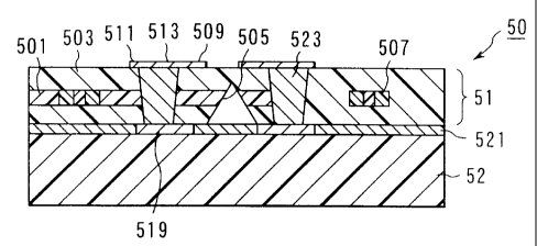
As shown in FIGS. 1 and 2, the optoelectric wiring
substrate 50 is composed of a substrate 52 and an
optical wiring layer 51 laminated thereon.
First, based on FIGS. 1 and 2, the configuration
of the optoelectric wiring substrate 50 will be
described in the order of an optical wiring system, an
electric wiring system, and a connection between the
optical and electric wiring systems.
An optical wiring layer 51 consists of a core 501
through which optical signals propagate and a clad 503
that confines optical signals in the core 501. Optical
signals propagate through the core 501 by increasing
the refractive index of a material forming the core 501
above that of the clad 503.
The core 501 has a mirror 505 installed in such a
manner that optical signals are incident at 45 .
Optical signals propagate between optical waveguides
and an optical part (a laser diodes and a photo diodes)
via a mirror 505 (see FIGS. 9A and 9B). An interface
of the mirror 505 (the surface opposite to the core 501
side ) is brought in contact with a resin having a
lower refractive index than the core 501 or with air.
Alternatively, a thin metal film may be formed on the
interface.
An optoelectric wiring substrate 53, which is
shown in FIG. 2B, shows another example concerning
formation of the mirror 505 installed in such a manner
CA 02302899 2000-03-29
- 23 -
that optical signals are incident at 450 . The
optoelectric wiring substrates 50 and 53 have the same
configuration except for formation of the mirror 505.
The optical wiring layer 51 has pads 509 arranged
on its surface and immediately over the mirror 505 in a
periphery thereof. The pads 509 electrically connect
the substrate 52 to the optical parts provided on the
optical wiring layer 51. The number of pads 509 is
determined by the number of optical parts installed.
Accordingly, the number is not limited to four as shown
in FIG. 1, but may be arbitrary. In addition, the
shape of the pads is determined by the shape of
connection terminals for the installed optical parts.
Thus, the shape is not limited to a circle as shown in
FIG. 1, but may be arbitrary. In general, the shape of
pads may correspond to the shape of solder balls,
metallic leads, or the like for connections with the
optical parts.
Further, the optical wiring layer 51 has lands 511
and an electric wiring 513 installed on its surface,
the electric wiring 513 connecting the lands 511 to the
pads 509.
The substrate 52 has an electric wiring 519 on its
surface. The substrate 52 may be a single-layer
insulating substrate or a multilayered electric wiring
substrate. The material of the substrate 52 may be a
polyimide film, a substrate comprised of a glass cloth
CA 02302899 2000-03-29
- 24 -
impregnated with an epoxy resin or the like, a ceramic
substrate, etc.
The optical wiring layer 51 is fixed to the
substrate 52 via an adhesive 521. In addition, the
optical parts provided on the optical wiring layer 51
and the electric wiring 519 are electrically connected
as follows:
That is, the lands 511 and the electric wiring 519
are electrically connected together via the via holes
523. A electric current from the electric wiring 519
is supplied to the lands 511 via the via holes 532 and
further to the pads 509 via an electric wiring 513.
The optical parts provided on the optical wiring layer
51 can obtain a required the electric current by means
of electric connections with the pads 509.
Although not shown, the electric parts and the
electric wiring on the substrate are similarly
electrically connected together.
In the optoelectric wiring substrate shown in
FIGS. 2A and 2B, the pads 509, the lands 511, and the
electric wiring 513 are exposed on the surface of the
optical wiring layer 51. On the contrary, optoelectric
wirings 55, 57 are shown in FIGS. 3A and 3B wherein the
lands 511 and electric wiring 513 on the surface of the
optical wiring layer 51 are coated with a resin layer
525 having the same refractive index as the clad 503
and wherein only the portion of the pad 5 for electric
CA 02302899 2007-11-30
29015-7
- 25 -
connections with the optical parts is exposed.
Differences between a method for rnanufacturing the
optoelectric substances (such as optoelectric substrates) 50,
53 and a method for manufacturing the optoelectric substances
(such as optoelectric substrates) 55, 57 and differences in
the effects of these substrates will be described below.
Although not shown in FIGS. 3A and 3B, the pads
for electric connections with the electric pads must be
similarly exposed.
Next, alignment of the optoelectric wiring
substrate according to the present invention will be
explained.
Since the present invention is the optoelectric
wiring substrate in which the optical parts are
mounted, alignment between the substrate and the
optical parts is important.
Thus, each of the optoelectric wiring substances
50, 53 , 55, 57 has alignment marks 507 formed thereon
for determining the positions of the pads 509 for
mounting the optical parts and alignment marks 515 for
determining the position of the mirror 505. These
alignment marks are formed simultaneously with the core
501 as described below.
Although not explained in this embodiment, the
alignment marks may be provided as required. If, for
example, aligriment marks 515 are not formed, the
surface of the optoelectric wiring substrate 59 on
CA 02302899 2000-03-29
- 26 -
which the optical parts are mounted is as shown in
FIG. 4.
2. Method for Manufacturing an optoelectric Wiring
Substrate
Next, a method for manufacturing an optoelectric
wiring substrate according to the present invention
will be explained.
A summary of the method for manufacturing an
optoelectric wiring substrate according to the present
invention will be given below.
First, an optical wiring layer is produced on a
support substrate that is separate from a substrate
having an electric wiring. At this point, a core and
alignment marks are simultaneously produced using the
photolithography technology.
Next, a mirror is provided in part of the core
using the alignment marks as references.
Next, the optical wiring layer is stuck to the
substrate.
Next, using the alignment marks as references,
pads are formed on the optical wiring layer, the pads
being electrically connected to the electric wiring on
the substrate via the via holes.
An import point of this manufacturing method is
that the method comprises the step of producing the
optical wiring layer on the separate support substrate
beforehand and the step of sticking this layer to the
CA 02302899 2000-03-29
- 27 -
electric wiring substrate. Thus, this method does not
include the step of producing an optical wiring by
directly stacking it on an insulated substrate having
recesses and projections as well as an electric wiring.
Due to these steps, the optical wiring layer serves to
lessen the effect of recesses and projections on the
underlying electric wiring substrate, thereby reducing
the loss of optical signals arising from this
unevenness.
Three examples of manufacturing methods will be
described below in further detail with reference to the
drawings.
<Method 1-1 for Manufacturing an optoelectric
wiring substrate>
A first example shows a method for manufacturing
an optoelectric wiring substrate 50, which is shown in
FIG. 2A. This method will be described below with
reference to FIGS. 5A to 50.
FIGS. 5A to 50 show each step of the method for
manufacturing the optoelectric wiring substrate 50 and
are arranged in the order of the steps.
First, as shown in FIG. 5A, a thin film layer of
Cr and Cu is sputtered as a release layer 531 on a
support substrate 559 that is a silicon wafer, and
about 101um of Cu layer is subsequently formed thereon
in a copper sulfate plating bath.
Next, as shown in FIG. 5B, Polyimide OPI-N1005
CA 02302899 2000-03-29
- 28 -
(manufactured by Hitachi Chemical Industry Inc.) is
spin-coated on the release layer 531 as a first clad
504 and imidized at 350 C. At this point, the film
thickness is, for example, about 20,um.
As shown in FIG. 5C, Polyimide OPI-N1305
(manufactured by Hitachi Chemical Industry Inc.) is
similarly spin-coated on the first clad 504 as a core
layer 532 and imidized at 350 C. At this point, the
film thickness is, for example, about 8,um. The
materials of the core 501 (core layer 532) and the
first clad 504 (the clad 503), which constitute an
optical wiring layer 51, need not necessarily be the
polyimide resins. The materials may be polymeric
materials such as fluorinated or deuterated epoxy
resins, ester methacrylate resins, or the like which
are subject to fewer losses in the wavelength of light
used for optical signals.
Further, Al is deposited on a surface of the core
layer 532, a predetermined photo resist pattern is
formed, and Al metal masks 533 and 535 are formed by
means of etching. The metal mask 533 corresponds to a
pattern of a core 501 that will be an optical wiring.
In addition, the metal mask 535 corresponds to a
pattern of alignment marks 507.
Next, as shown in FIG. 5D, an oxygen gas is used
to etch the core layer 532 by means of reactive ion
etching. Further, the Al film, which is the metal
CA 02302899 2000-03-29
- 29 -
masks, is etched off to simultaneously form the pattern
of the core 501 (optical wiring) and the pattern of the
alignment marks 507. At this point, the line width of
the core 501 pattern is, for example, 8 m. In
addition, its cross section is a square, for example,
8,u m in height and 8,u m in width. The size of the cross
section of the core 501 are not limited to this but may
be between 5 and 100,um depending on differences in
transmission mode and in refractive index between the
core and the clad.
As shown in FIG. 5E, OPI-1005 is coated and
imidized as a second clad 506. This step is similar to
that for the first clad 504. At this point, the clad
has a thickness of 20,um, for example, on the core
optical wiring layer. Thus, the clad 503 which
comprises the first clad 504 and the second clad 506 is
formed
Then, as shown in FIG. 5F, a thin metal film of Cr
and Cu is sputtered on a surface of the second clad
506. In addition, about 10gm of a Cu layer is formed
in a copper sulfate plating bath. Further, a photo
resist pattern is formed using the photolithography
technique, and is etched using an etchant. As a
result, pads 509, an electric wiring 513, and lands 511
can be formed. Previously formed openings 537 are
shown with the lands 511 in FIG. 5E. Hole sections for
forming via holes 523 are formed later in these
CA 02302899 2007-11-30
29015-7
- 30 -
openings 537 by means of a laser. In addition,
although not shown, at the same time, pads, an electric
wiring, arid lands for connections with electric parts
are formed.
Next, a photo resist 539 is coated as a protect
film as shown in FIG. 5G. This film protects the pads,
509, electric wiring 513, and lands 511, which are
formed of copper, from a release agent.
Next, the Cu layer in the release layer 531 is
dissolved using a ferric chloride liquid as a release
agent, and the optical wiring layer is released to
produce an optical wiring film, as shown in-FIG. 5H.
As shown in FIG. 51, the side of the optical
wiring layer 51 on which the pads 509, the electric
wiring 513, and the lands 511 are formed is stuck to a
second support 541 using an adhesive. In this case,
the second support 541 had better be transparent so
that the alignment marks 507 can be seen from the side
of the optical wiring layer 51 which is not stuck to
the second support. In addition, the adhesive must be
easy to release or be likely to have its adhesive
strength reduced when hardened by means of ultraviolet
rays.
As shown in FIG. 5J, in forming the core 501
pattern, a mirror 505 is mechanically formed in part of
the core 501 pattern at an angle of 450 relative to the
substrate 52 using the alignment marks (refer to
CA 02302899 2000-03-29
- 31 -
FIG. 4) as references.
As shown in FIG. 5K, as an adhesive 521, a
modified polyimide resin exhibiting a thermal
plasticity is coated and dried on the substrate 52 with
the electric wiring 519. Then, the surface of the
optical wiring layer on which the mirror has been
formed is stuck to the substrate 52 and heated for
adhesion.
Next, the structure is irradiated with ultraviolet
rays to release the second support 541, as shown in 5L.
Then, a plated resist 543 is coated on the optical
wiring layer 51 as a protect film, as shown in FIG. 5M.
As shown in FIG. 5N, at the openings 537 of the
lands 511, which correspond to positions at which the
via holes 523 are to be formed, holes 545 for the via
holes 523 are formed by means of a laser. In this
case, suitable lasers include an excimer laser, a
carbon dioxide laser, a YAG laser, etc.
As shown in FIG. 50, a thin metal film of Cr and
Cu is sputtered on the surface of the optical wiring
layer 51 and on internal surfaces of the laser-
processed holes 545. Then, this thin metal film is
used as an electrode to plate the inside of the via
holes 523 and the land 511 sections with copper in a
copper sulfate plating bath. Finally, the plated
resist 543, which is a protect film, is removed, and
the via holes 523 and the lands 511 are formed to
CA 02302899 2000-03-29
- 32 -
obtain the optoelectric wiring substrate 50 shown in
FIG. 2A.
<Method 2 for Manufacturing an optoelectric wiring
substrate>
A second example of a method for manufacturing an
optoelectric wiring substrate is another method for
manufacturing the optoelectric wiring substrate 50
shown in FIG. 2A. This method will be described below
with reference to FIGS. 6A to 6M.
FIGS. 6A to 6M show each step of this method for
manufacturing the optoelectric wiring substrate 50 and
are arranged in the order of the steps.
First, as shown in FIG. 6A, a thin film layer of
Cr and Cu is sputtered as a release layer 531 on a
substrate 52 that is a silicon wafer, and about 10,um of
Cu layer is subsequently formed thereon in a copper
sulfate plating bath.
Next, as shown in FIG. 6B, Polyimide OPI-N1005
(manufactured by Hitachi Chemical Industry Inc.) is
spin-coated on the release layer 531 as a first clad
504 and imidized at 350 C. At this point, the film
thickness is, for example, about 20g m.
As shown in FIG. 6C, Polyimide OPI-N1305
(manufactured by Hitachi Chemical Industry Inc.) is
similarly spin-coated on the first clad 504 as a core
layer 532 and imidized at 350 C. At this point, the
film thickness is, for example, about 8,um. The
CA 02302899 2000-03-29
- 33 -
materials of the core 501 (core layer 532) and clad
503, which constitute an optical wiring layer, need not
necessarily be the polyimide resins. The materials may
be polymeric materials such as fluorinated or
deuterated epoxy resins, ester methacrylate resins, or
the like which are subject to fewer losses in the
wavelength of light used for optical signals.
Further, Al is deposited on a surface of the core
layer 532, and a predetermined photo resist pattern is
formed and etched to form Al metal masks 533 and 535.
The metal mask 533 corresponds to a pattern of a core
501 that will be an optical wiring. In addition, the
metal mask 535 corresponds to a pattern of alignment
marks 507.
Next, as shown in FIG. 6D, an oxygen gas is used
to etch the core layer 532 by means of reactive ion
etching. Further, the Al film, which is the metal
masks, is etched off to simultaneously form the pattern
of the core 501 (optical wiring) and the pattern of the
alignment marks 507. At this point, the line width of
the core 501 pattern is, for example, 8g m. In
addition, its cross section is a square, for example,
8,u m in height and 8 m in width. The size of the cross
section of the core 501 are not limited to this but may
be between 5 and 100,um depending on differences in
transmission mode and in refractive index between the
core and the clad.
CA 02302899 2000-03-29
- 34 -
As shown in FIG. 6E, OPI-1005 is coated and
imidized as a second clad 506. This step is similar to
that for the first clad 504. At this point, the clad
has a thickness of 20,um, for example, on the core
optical wiring layer.
Then, as shown in FIG. 6F, in forming the core 501
pattern, a mirror 505 is mechanically formed in part of
the core 501 pattern at an angle of 450 relative to the
substrate 52 using the simultaneously formed alignment
marks (refer to FIG. 4) as references.
Next, the Cu layer in the release layer is
dissolved using a ferric chloride liquid as a release
agent, and the optical wiring layer is released to
produce an optical wiring film, as shown in FIG. 6G.
As shown in FIG. 6H, as an adhesive 521, a
modified polyimide resin exhibiting thermal plasticity
is coated and dried on the substrate 52 with the
electric wiring 519. Then, the surface of the optical
wiring layer on which a mirror has been formed is stuck
to the substrate 52 and heated for adhesion.
As shown in FIG. 61, at positions at which via
holes 523 are to be formed, holes 545 are formed by
means of a laser. In this case, suitable lasers
include an excimer laser, a carbon dioxide laser, a YAG
laser, etc.
As shown in FIG. 6J, a thin metal film 547 of Cr
and Cu is sputtered on a surface of the optical wiring
CA 02302899 2000-03-29
- 35 -
layer 51 and on internal surfaces of the laser-
processed holes 545.
A plated resist pattern 543 (protect film 549) is
formed on the optical wiring layer surface except for
pads 509, lands 511, and an electric wiring 513, as
shown in FIG. 6K.
As shown in FIG. 61, the thin metal film 547 is
used as an electrode to plate the inside of the via
holes 523, the pads 509, the lands 511, and the
electric wiring 513 with copper in a copper sulfate
plating bath.
As shown in FIG. 6M, the plated resist 543 is
removed and the thin metal film 547 is further removed
by means of soft etching. Then, the via holes 523, the
pads 509, the lands 511, and the electric wiring are
formed to obtain the optoelectric wiring substrate 50.
<Method 3 for Manufacturing an optoelectric wiring
substrate>
A third example of a method for manufacturing an
optoelectric wiring substrate is a method for
manufacturing an optoelectric wiring substrate 53,
which is shown in FIG. 2B. This method will be
described below with reference to FIGS. 7A to 7P.
FIGS. 7A to 7P show each step of the method for
manufacturing the optoelectric wiring substrate 53 and
are arranged in the order of the steps.
First, as shown in FIG. 7A, a thin film layer of
CA 02302899 2000-03-29
- 36 -
Cr and Cu is sputtered as a release layer 531 on a
substrate 52 that is a silicon wafer, and about l0,um of
Cu layer is subsequently formed thereon in a copper
sulfate plating bath.
Next, as shown in FIG. 7B, Polyimide OPI-N1005
(manufactured by Hitachi Chemical Industry Inc.) is
spin-coated on the release layer 531 as a first clad
504 and imidized at 350 C. At this point, the film
thickness is, for example, about 20 m.
As shown in FIG. 7C, Polyimide OPI-N1305
(manufactured by Hitachi Chemical Industry Inc.) is
similarly spin-coated on the first clad 504 as a core
layer 532 and imidized at 350 C. At this point, the
film thickness is, for example, about 8/cm. The
materials of the core 501 (core layer 532) and clad
503, which constitute an optical wiring layer, need not
necessarily be the polyimide resins. The materials may
be polymeric materials such as fluorinated or
deuterated epoxy resins, ester methacrylate resins, or
the like which are subject to fewer losses in the
wavelength of light used for optical signals.
Further, Al is deposited on a surface of the core
layer 532, and a predetermined photo resist pattern is
formed and etched to form Al metal masks 533 and 535.
The metal mask 533 corresponds to a pattern of a core
501 that will be an optical wiring. In addition, the
metal mask 535 corresponds to a pattern of alignment
CA 02302899 2000-03-29
- 37 -
marks 507.
Next, as shown in FIG. 7D, an oxygen gas is used
to etch the core layer 532 by means of reactive ion
etching. Further, the Al film, which is the metal
masks, is etched off to simultaneously form the pattern
of the core 501 (optical wiring) and the pattern of the
alignment marks 507. At this point, the line width of
the core 501 pattern is, for example, 8,u m. In
addition, its cross section is a square, for example,
8ccm in height and 8,u m in width. The size of the cross
section of the core 501 are not limited to this but may
be between 5 and 1001im depending on differences in
transmission mode and in refractive index between the
core and the clad.
As shown in FIG. 7E, OPI-1005 is coated and
imidized as a second clad 506. This step is similar to
that for the first clad 504. At this point, the clad
has a thickness of 20u m, for example, on the core
optical wiring layer.
As shown in FIG. 7F, a thin metal film of Cr and
Cu is sputtered on a surface of the second clad 506.
In addition, about 10 m of a Cu layer is formed in a
copper sulfate plating bath. Further, a photo resist
pattern is formed using the photolithography technique,
and is etched using an etchant. As a result, pads 509,
an electric wiring 513, and lands 511 can be formed.
Previously formed openings 537 are shown with the lands
CA 02302899 2000-03-29
- 38 -
511 in FIG. 7E. In these openings 535, hole sections
for forming via holes 523 are formed later by means of
a laser. In addition, although not shown, at the same
time, pads, an electric wiring, and lands for
connections with an electric part are formed.
Next, a photo resist 539 is coated as a protect
film as shown in FIG. 7G. This film protects the pads,
509, electric wiring 513, and lands 511, which are
formed of copper, from a release agent.
Next, the Cu layer in the release layer 22 is
dissolved using a ferric chloride liquid as a release
agent, and the optical wiring layer 51 is released to
produce an optical wiring film, as shown in FIG. 7H.
As shown in FIG. 71, a side of the optical wiring
layer 51 on which the pads 509, the electric wiring
513, and the lands 511 are formed is stuck to a second
support 541 using an adhesive. In this case, the
second support 541 had better be transparent so that
the alignment marks 507 can be seen from its side to
which the optical wiring layer 51 is not stuck. In
addition, the adhesive must be easy to release or tend
to have its adhesive strength reduced when hardened by
means of ultraviolet rays.
Further, in FIG. 71, a thin film layer of Cr and
Cu is sputtered on the surface of the optical wiring
layer 51 opposite to its stuck surface, and l0,um of a
Cu layer is formed thereon in a copper sulfate plating
CA 02302899 2000-03-29
- 39 -
bath. Furthermore, a photo resist pattern is formed
using the photolithography technique, and is etched
using an etchant to form a laser mask 551 for forming a
mirror. The position of the laser mask 551 is defined
by the alignment marks 507 similarly to the pads 509 on
the opposite surface. In addition, openings 553 are
formed in the laser mask. Accordingly, with
irradiation with laser light, only the openings 553 are
processed.
Then, by irradiating the openings 553 with laser
light in such a manner that the incident angle is 45
relative to the substrate surface, a mirror 512 is
formed at an angle of 450 relative to the substrate
541, as shown in FIG. 7J. In this case, suitable
lasers include an excimer laser, a carbon dioxide
laser, a YAG laser, etc.
As shown in FIG. 7K, the laser mask 551 is removed
using an etchant.
As shown in FIG. 7L, as an adhesive, a modified
polyimide resin 521 exhibiting thermal plasticity is
coated and dried on the substrate 52 with the electric
wiring 519. Then, the surface of the optical wiring
layer on which the mirror has been formed is stuck to
the substrate 52 and heated for adhesion.
Next, the structure is irradiated with ultraviolet
rays to release the second support 541, as shown in 7M.
Then, a plated resist 543 is coated on the optical
CA 02302899 2000-03-29
- 40 -
wiring layer 51 as a protect film, as shown in FIG. 7N.
As shown in FIG. 70, at the openings 537 of the
lands 511, which correspond to positions at which via
holes 523 are to be formed, holes 555 are formed by
means of a laser. In this case, suitable lasers
include an excimer laser, a carbon dioxide laser, a YAG
laser, etc.
As shown in FIG. 7P, a thin metal film of Cr and
Cu is sputtered on the surface of the optical wiring
layer 51 and on the inside of the laser-processed
holes. Then, this thin metal film is used as an
electrode to plate the inside of the via holes 523 and
the lands 511 with copper in a copper sulfate plating
bath. Furthermore, the plated resist 543, which is a
protect film, is removed, and the via holes 523 and the
lands 511 are formed to obtain the optoelectric wiring
substrate 53.
In addition, although not described in detail, in
the step shown in FIG. 7F, while forming the pads 509,
the lands 511, and the electric wiring 513, a mirror
can be formed by forming a laser mask for mirror
formation and irradiating the mask with laser light
with an incident angle of 450 relative to the
substrate. This simplifies the steps and enables the
positions of the pads and mirror to be accurately
determined using the single photo mask.
<Method 1-4 for manufacturing an optoelectric
CA 02302899 2000-03-29
- 41 -
wiring substrate>
A method 1-4 for manufacturing an optoelectric
wiring substrate is a method for manufacturing an
optoelectric wiring substrate 55, which is shown in
FIG. 3A. The method will be explained referring to
FIGS. 8A and 8B.
The optoelectric wiring substrate 55 is formed by
providing a resin layer 525 (having the same refractive
index as the clad 503) on the optoelectric wiring layer
50 as described above. Thus, the fourth manufacturing
method is the first manufacturing method with addition
of new steps for manufacturing the resin layer 525.
Description of the same steps as in the first
manufacturing method is omitted below, and only the new
additional steps will be explained.
FIGS. 8A and 8B show the steps for manufacturing
the resin layer 525 which are continued from FIG. 50,
and are arranged in the order of the steps.
After manufacturing the optoelectric wiring
substrate 50 in the step shown in FIG. 50, as shown in
FIG. 8A, Polyimide OPI-N1005 (manufactured by Hitachi
Chemical Industry Inc.), which has been used for the
clad 503, is spin-coated on the surface of the optical
wiring layer 50 and imidized at 350 C. At this point,
the film thickness is, for example, about 10,um.
Finally, as shown in FIG. 8B, the pads 509 are
irradiated with laser light using the alignment marks
CA 02302899 2000-03-29
- 42 -
507 as references, thereby removing the polyimide from
the pads 509. As a result, openings 556 are formed.
In this case, preferable lasers include an excimer
laser, a carbon dioxide laser, a YAG laser, etc.
As a result, the optoelectric wiring substrate 55
can be obtained.
The optoelectric wiring substrate 55, 57 can also
be produced using the following method: The second and
third manufacturing method include the additional steps
wherein after completion of each optoelectric wiring
substrate, the Polyimide OPI-N1005 (manufactured by
Hitachi Chemical Industry Inc.) layer, which has been
used for the clad 503, is formed on the optical wiring
layer and the polyimide is then removed from the pads.
3. Mounted Substrate
A mounted substrate in which an optical part (a
light-emitting element, a light-receiving element, or
the like) is mounted on the optoelectric wiring
substrate will be described below. The mounted
substrate will be explained below by taking an
optoelectric wiring substrate 55 by way of example, but
this invention is applicable to other optoelectric
wiring substrates.
FIG. 9A shows a mounted substrate 60 in which a
light-emitting element 58 is mounted on the
optoelectric wiring substrate 55.
A laser beam 100 emitted from a light-emitting
CA 02302899 2000-03-29
- 43 -
surface 581 of a light-emitting element 131 is
reflected by a mirror 505 and then propagates through a
core 501 in an optical wiring layer 506.
FIG. 9B shows a mounted substrate 62 in which a
light-emitting element 59 is mounted on the
optoelectric wiring substrate 55.
The laser beam 100, which has propagated through
the core 501 in the optical wiring layer 56, is
reflected by the mirror 505 and then impinges on a
light-receiving surface 591 of the light-receiving
element 59.
FIG. 10 shows the mounted substrate 62 in which a
BGA package 66, an electric part, is mounted on an
optoelectric wiring substrate .
The above optical and electric parts and the
optoelectric wiring substrate are electrically
connected together using solder balls 557. In
addition, if the optical part has metal leads, the
electric connection is made by soldering pads 509 and
the optical part together.
Next, alignment between the mounted substrate and
the optical and electric parts.
As described above, each of the above
manufacturing methods enables the core 501 and
alignment marks 507, 515 to be simultaneously formed.
Then, the alignment marks 507, 515 can be used as
references to accurately determine a position of the
CA 02302899 2000-03-29
- 44 -
mechanically formed mirror 505 or a position of a
mirror 512 formed using a laser mask.
In addition, in mounting the pads 506 and the
optical and electric parts on the optoelectric wiring
substrate, a self alignment effect of solder used for
joining allows a position of the light-emitting or
light-receiving surface of the optical part to be
accurately determined.
Further, if a resin layer 525 of a material having
the same refractive index as the clad is formed on a
surface of an optical wiring layer 56, 58, the
following alignment effect can further be obtained: As
described in the step shown in FIG. 8B, by removing the
resin from the pad surfaces by means of a laser using
the alignment marks 507 as references, the optical part
can be more accurately aligned during soldering of the
solder balls or leads. That is, since soldering of the
solder balls or leads are put in openings 556
accurately aligned based on the alignment marks 507,
the optical part or the like mounted on the
optoelectric wiring substrate can be more accurately
aligned.
Consequently, simply by mounting the electric and
optical parts on the optoelectric wiring substrate
through a reflow furnace, the alignment between optical
axes of the optical part and a waveguide can be
performed accurately. As a result, precise
CA 02302899 2000-03-29
- 45 -
optoelectric wiring substrates and mounted substrates
can be obtained without the needs for advanced manual
work, thereby enabling cost reduction and mass
production.
The above configuration provides the following
effects:
First, high-density mounting and size reduction
can be achieved. This is because the optical wiring
layer is laminated on the substrate with the electric
wiring.
Second, the locational relationship between the
core acting as the optical wiring, the pads installed
an optical part or the like and the mirror can be
extremely approximated to the design. This is because
the optoelectric wiring substrate and mounted substrate
according to the present invention have the above
mentioned alignment effects to enable the optical axes
of the optical part and the core acting as the optical
wiring to be optically aligned easily.
Third, cost reduction and mass production can be
attained compared to the prior art. This is because
the above configurations require no manual work that
requires experiences for optical-axis alignment and the
like.
Forth, the optoelectric wiring substrate according
to the present invention further enables the electric
wiring to be formed on the optical wiring layer.
CA 02302899 2000-03-29
- 46 -
Accordingly, cross talk between the electric wires can
be restrained. As a result, noise can be reduced.
Fifth, the optical propagation loss of the core
can be reduced. The reason is as follows: After being
manufactured on the flat support, the optical wiring
layer according to the present invention is stuck to
the substrate with the electric wiring. Thus, the
effect of recesses and projections of the electric
wiring on the substrate can be lessened compared to an
optical wiring layer directly manufactured on a
substrate (with an electric wiring).
(SECOND EMBODIMENT)
Next, a second embodiment will be explained.
The second embodiment can provide a higher
alignment effect in manufacturing an optoelectric
wiring substrate. In the following example, for
simplicity, a method in which a mirror 505, 512 for
reflecting laser light is not formed is taken by way of
example. Adding a known mirror formation step to the
manufacturing method described below enables an
optoelectric wiring substrate with a mirror to be
manufactured easily.
Two examples of manufacturing methods will be
described below with reference to the drawings.
<Method 2-1 for Manufacturing an optoelectric
Wiring Substrate>
A first example of a method for manufacturing an
CA 02302899 2000-03-29
- 47 -
optoelectric wiring substrate according to second
embodiment will be described with reference to
FIGS. 11A to 11N. The resulting optoelectric wiring
substrate is a substrate 70, which is shown in
FIG. 11N.
FIGS. 11A to 11N show each step of this
manufacturing method and are arranged in the order of
the steps.
First, as shown in FIG. 11A, a thin film layer of
Cr and Cu is sputtered as a release layer 531 on a
first support substrate 559 that is a silicon wafer or
the like, and about 1 m of Cu layer is subsequently
formed thereon in a copper sulfate plating bath.
Polyimide OPI-N1005 (manufactured by Hitachi Chemical
Industry Inc.) is spin-coated on the release layer 531
as a clad layer 561 and imidized at 350 C. At this
point, the film thickness is, for example, about 15/tm.
The first support substrate 559 is not limited to a
silicon wafer but may be a robust material having
smooth surfaces and which can resist a high temperature
of about 400 C.
Next, as shown in FIG. 11B, Polyimide OPI-N1305
(manufactured by Hitachi Chemical Industry Inc.) is
similarly spin-coated on the first clad 504 as a core
layer 532 and imidized at 350 C. At this point, the
film thickness is, for example, about 8,um.
Then, Al is deposited on a surface of the core
CA 02302899 2000-03-29
- 48 -
layer 532, and a predetermined photo resist pattern is
formed and etched to form aluminum metal masks.
Further, as shown in FIG. 11C, an oxygen gas is used to
etch part of the core layer 532 by means of reactive
ion etching. Likewise, an oxygen gas is used to etch
off the aluminum film to form a core 532 that will be
an optical wiring. Simultaneously with the formation
of the core 501, alignment marks (not shown) are formed
on the core layer 532. These alignment marks act as
references for sticking this substrate to an electric
wiring substrate, which will be described below.
As shown in FIG. 11D, OPI-N1005 is spin-coated on
the core 501 as a second clad 506 and imidized. At
this point, the film thickness of the second clad 506
newly formed on the core 501 is, for example, about
15gm (which is the same as the film thickness of the
clad layer 561 formed in the step shown in FIG. 11A).
As a result, an optical wiring layer 67 can be obtained
which consists of the core 501 and a clad 503, which
buries the core 501.
Next, a ferric chloride is used to dissolve and
remove a release layer 531 to release an optical wiring
layer 67, as shown in FIG. 11E.
Next, the step of sticking the optical wiring
layer 67 to the electric wiring substrate 52 will be
described with reference to FIGS. 11F to 11I.
An electric wiring 519 is formed on the top
CA 02302899 2000-03-29
- 49 -
surface of the electric wiring substrate 52. The
electric wiring 519 generates recesses and projections
which correspond to a difference in height of about
18/cm on the top surface of substrate 52.
The conventional manufacturing method directly
forms the optical wiring layer on the surface of the
electric wiring substrate 52. Consequently, the
optical wiring layer is affected by the unevenness of
the surface, resulting in reduced accuracy. The
manufacturing method according to the present invention
solves this problem by executing the steps described
below.
First, as shown in FIG. 11F, l,um of a first
adhesive 573 is coated on a second support substrate
541 made of glass, and the optical wiring layer 67 is
stuck to the second support substrate 541 using a
laminator. At this point, alignment between the second
support substrate 541 and the optical wiring layer 67
is not required. This is because the laminator makes
the surface of the optical wiring layer 67 very smooth.
The second support substrate 541 may be any
substrate made of glass or the like which has a certain
level of strength and which is flat and transparent.
In addition, the substrate is heated or irradiated with
ultraviolet rays as required depending on the type of
the adhesive.
This manufacturing method uses a polyimide
CA 02302899 2000-03-29
- 50 -
multilayer wiring substrate as the electric wiring
substrate 52. The electric wiring 519 is formed on the
top surface of the substrate 52. The electric wiring
substrate 52 is not limited to the polyimide multilayer
wiring substrate but may be a single-layer insulated
substrate or a multilayer wiring substrate with
electric wirings and insulated layers alternately
laminated together. In addition, the material may be
an insulated substrate comprised of a glass cloth
impregnated with a resin, a polyimide film, or a
ceramic substrate.
About 20gm of a second adhesion layer 577 is
formed on the electric wiring substrate 575.
Specifically, this layer can be formed by applying to
the substrate a modified polyimide resin exhibiting
thermal plasticity, followed by drying.
A preferable material of the second adhesion layer
577 is a thermal plastic adhesive, for example, an
ethylene-ester acrylate copolymer, a styrene-poly
(metha) ester acrylate, a butyral resin, a polyamide-
based resin, or a modified polyimide resin. The reason
why this manufacturing method employs the modified
polyimide resin is that the range of sticking
temperature is between 250 and 300 C, which is
preferable in terms of the heat resistance of solder on
an optoelectric wiring substrate.
The optical wiring layer 67 must be released from
CA 02302899 2000-03-29
- 51 -
the second support substrate 541 together with a first
adhesion layer 573. Thus, the design of this structure
must be such that the adhesion strength with which the
second adhesion layer 577 adheres to the optical wiring
layer 67 is larger than the adhesion strength with
which the first adhesion layer 573 adheres to the
optical wiring layer 67.
Alignment marks (not shown) are formed on the
electric wiring substrate 52, which is coated with the
second adhesion layer 577. These alignment marks are
provided at positions corresponding to the alignment
marks formed in the step corresponding to FIG. 11C. As
shown in FIG. 11G, the alignment marks formed on the
electric wiring substrate 52 are aligned with the
corresponding alignment marks formed on the optical
wiring layer 52 stuck to the second support substrate
541 (glass substrate), through the glass substrate, in
order to determine the positions of theses alignment
marks.
That is, as described above, the second support
substrate 541 is the transparent glass substrate. The
glass substrate and the optical wiring layer 67 allow
visible light to permeate therethrough smoothly, and
the first adhesion layer 573 has a sufficiently small
thickness. Consequently, the alignment marks of the
optical wiring layer 67 and electric wiring substrate
52 can be visually checked from the rear surface (the
---- - ------- -
CA 02302899 2000-03-29
- 52 -
surface opposite to the stuck side) of the second
support substrate 577.
Next, in FIG. 11H, the structure is heated at 250 C
for one hour while applying a pressure P thereto from
the rear surface of the second support substrate 541.
In this case, the adhesion can be carried out with a
reduced atmospheric pressure as required. If the
second adhesion layer 577 tends to be hardened when
exposed to electron beams or the like, it can be stuck
to the optical wiring layer by irradiating it with
electron beams from the second support substrate 541.
Then, as shown in FIG. 11I, the second support
substrate 541 is released from the optical wiring layer
together with the first adhesion layer 573 to complete
the sticking of the electric wiring substrate 52 and
the optical wiring layer 67.
It should be noted that the optical wiring layer
67 can be stuck and fixed to the electric wiring
substrate 52 while maintaining its smoothness and
without being affected by the unevenness of the
underlying electric wiring substrate 52. This can be
achieved by the steps in FIGS. 11F to 11I.
Next, the steps carried out before the
optoelectric wiring substrate according to the present
invention is completed will be described. The
remaining step forms pads for mounting an optical or
electric part on the optical wiring layer 67 stuck to
CA 02302899 2000-03-29
- 53 -
the electric wiring substrate 52 and via holes for
electrically connecting the optical part with the
electric wiring substrate.
As shown in FIG. 11J, a laser is used to form a
hole section 570 for via hole 523 formation using the
alignment marks (not shown) on the electric wiring
substrate 52. The method for forming the hole section
570 may be perforation using a carbon dioxide laser, a
UV-YAG laser, an excimer laser, or dry etching such as
reactive ion etching. In this case, the underlying
electric wiring 519 acts as a stopper for the
penetration.
Next, as shown in FIG. 11K, a sputter is used to
form thin metal films (not shown) in the order of Cr
and Cu. Furthermore, 10pm of PMER (manufactured by
Tokyo Applied Chemical Industry Co., LTd.) is coated on
the films using a spin coater, and is then dried at 90 C
to form a photo resist 541.
Then, as shown in FIG. 11L, a photo mask having a
predetermined pattern is used to carry out exposure and
development using as references the alignment marks
(not shown) formed on the electric wiring substrate 52.
Then, an opening 570 for via hole 523 formation and an
opening 575 for pad formation are produced. Further,
post-baking is executed at 110 C.
As shown in FIG. 11M, the thin metal films (see
the description of the step shown in FIG. 11K) are used
CA 02302899 2000-03-29
- 54 -
as a negative electrode to form a plated film 576 in a
copper sulfate bath. The plated film 576 is, for
example, 10,um in thickness, which is substantially
equal to the thickness of the photo resist.
Finally, as shown in FIG. 11N, the photo resist
571 is removed by means of an exclusive release agent,
and the thin metal films are dissolved and removed by
means of an etchant to produce via holes 523 and pads
519. Thus, an optoelectric wiring substrate 70
according to the present invention can be completed.
<Method 2-2 for Manufacturing an optoelectric
Wiring Substrate>
Next, a second example of a method for
manufacturing an optoelectric wiring substrate
according to second embodiment will be described. This
method is an another method for manufacturing the
optical wiring layer on the transparent support
substrate, which is similar to the manufacturing method
2-1. The resulting optoelectric wiring substrate is a
substrate 70, which is shown in FIG. 11N.
FIGS. 12A to 12G show each step of the sixth
manufacturing method and are arranged in the order of
execution.
First, an optical wiring layer is manufactured. A
thin film layer of Cr and Cu is sputtered on a third
support substrate 584 made of glass or the like, to
form a release layer 563 as shown in FIG. 12A. The
CA 02302899 2000-03-29
- 55 -
third support substrate 584 is not limited a glass
substrate but may be any robust substrate that has
smooth surfaces, that can resist a temperature of about
400 C, and that allows visible light to permeate
therethrough smoothly. These characteristics are
common to a second substrate 541.
Subsequently, about l,um of a Cu layer is formed in
a copper sulfate plating bath (not shown). The photo
etching method, a specified method, is used to form
alignment marks (not shown) at predetermined positions
of this thin metal film layer. The alignment marks are
used as alignment references in sticking the optical
wiring layer to an electric wiring substrate, which
will be described below.
Next, Polyimide OPI-N1005 (manufactured by Hitachi
Chemical Industry Inc.) is similarly spin-coated on the
Cu layer and imidized at 350 C to form a clad 504 as
shown in FIG. 12A. At this point, the clad 504 has a
thickness, for example, of about 15/tm.
Next, Polyimide OPI-N1305 (manufactured by Hitachi
Chemical Industry Inc.) is similarly spin-coated on the
clad layer 561 and imidized at 350 C to form a core
layer 532 as shown in FIG. 12B. At this point, the
core layer 532 has a thickness, for example, of about
8 g m.
Then, aluminum is deposited on a surface of the
core layer 532, and a predetermined photo resist
CA 02302899 2000-03-29
- 56 -
pattern is formed and etched to form Al metal masks.
Further, an oxygen gas is used to etch the core layer
532 by means of reactive ion etching in order to remove
the aluminum film. As a result, a core 501 is obtained
as shown in FIG. 12C. At this point, alignment marks,
which are used to improve an accuracy of sticking with
the substrate 52, are formed simultaneously.
Next, Polyimide OPI-N1005 is similarly coated on
the core 501 and part of the clad 504 and imidized at
350 C to form a clad 503, which buries the core 501.
The clad layer newly laminated in this step has a
thickness of 15 m, for example, on the core 501.
These steps result in an optical wiring layer 67.
Next, each of the steps of sticking the optical wiring
layer 67 and the electric wiring substrate 52 together
will be described based on FIGS. 12E to 12G.
First, about 20 m of a second adhesion layer 577
is formed on an electric wiring substrate 52.
Specifically, this layer can be formed by applying to
the substrate a modified polyimide resin exhibiting
thermal plasticity, followed by drying.
A preferable material of the second adhesion layer
577 is a thermal plastic adhesive, for example, an
ethylene-ester acrylate copolymer, a styrene-poly
(metha) ester acrylate, a butyral resin, a polyamide-
based resin, or a modified polyimide resin. The reason
why this manufacturing method employs the modified
CA 02302899 2000-03-29
- 57 -
polyimide resin is that the range of sticking
temperature is between 250 and 300 C, which is
preferable in terms of the heat resistance of solder on
an optoelectric wiring substrate.
Alignment marks (not shown) are formed on the
electric wiring substrate 52, which is coated with the
second adhesion layer 577. These alignment marks are
provided at positions corresponding to the alignment
marks formed in the step corresponding to FIG. 12C. As
shown in FIG. 12E, the alignment marks formed on the
electric wiring substrate 52 are aligned with the
corresponding alignment marks formed on the optical
wiring layer stuck to the second support substrate 541
(glass substrate), through the glass substrate, in
order to determine the positions of theses alignment
marks.
In this case, a third support substrate 584 has
characteristics similar to those of the second support
substrate 541 described in the fifth manufacturing
method. Accordingly, alignment between the optical
wiring layer 67 and the electric wiring substrate 52
can be executed easily.
Next, as shown in FIG. 12H, the structure is
heated at 250 C for one hour while applying a pressure P
thereto from a rear surface (a surface opposite to the
stuck side) of the third support substrate 584. In
this case, the adhesion can be carried out with a
CA 02302899 2000-03-29
- 58 -
reduced atmospheric pressure as required. If the
second adhesion layer 577 tends to be hardened when
exposed to electron beams or the like, it can be stuck
to the optical wiring layer by irradiating it with
electron beams from the third support substrate 584.
Then, the release layer 531 is dissolved and
removed by means of a ferric chloride liquid to release
the third support substrate 584, as shown in FIG. 12G.
These steps complete the sticking of the electric
wiring substrate 52 and the optical wiring layer 67.
The subsequent steps (formation of pads, via
holes, and other components) are similar to those of
the above manufacturing method 2-1 which are shown in
FIGS. 11J to 11N.
This manufacturing method 2-2 enables an
optoelectric wiring substrate 70 to be obtained.
According to the manufacturing method 2-2, the optical
wiring layer 67 can also be stuck and fixed to the
electric wiring substrate 52 while maintaining the
smoothness of the third support substrate 584 and
without being affected by the unevenness of the
electric wiring substrate 52.
The above configuration can provide the following
effects:
The optical wiring layer of the optoelectric
wiring substrate is not affected by the unevenness of
the underlying electric wiring substrate surface. The
CA 02302899 2000-03-29
- 59 -
propagation loss of optical signals can be minimized.
This is because the optical wiring layer is fixed to
the smooth support substrate so as to be stuck to the
electric wiring substrate while maintaining its
smoothness.
Since during the sticking between the optical
wiring layer and the electric wiring substrate, the
alignment marks on the optical wiring layer and
electric wiring substrate can be read easily, thereby
enabling accurate sticking. This is because each of
the support substrates is comprised of a transparent
material. As a result, the electric wiring can be
accurately aligned with pads for mounting an optical
part.
A mounted substrate in which an optical part (a
light-emitting element, a light-receiving element, or
the like) is mounted on the optoelectric mounted
substrate 70 described in the second embodiment can be
manufactured using steps similar to those of the
mounted-substrate manufacturing method already
described in the first embodiment.
Next, a third example will be explained.
(Third embodiment)
Next, a third embodiment will be explained.
The third embodiment describes another type of
optoelectric wiring substrate and a manufacturing
method therefor.
CA 02302899 2000-03-29
- 60 -
An important point of the optoelectric wiring
substrate shown in the third embodiment is the concept
that an optical wiring layer on which an optical part
(optical element) is mounted is laminated on a
substrate having an electric wiring, as in the first
embodiment.
Further, an important point of the manufacturing
method shown in the third embodiment is the concept
that a core acting as an optical wiring, a pad pattern,
and alignment marks are simultaneously manufactured.
The third embodiment will be described below with
reference to the drawings.
FIG. 13 shows a top view showing an optoelectric
wiring substrate 70 according to the third embodiment
as seen from an optical part-mounted side.
FIG. 14A is a sectional view taken along the
direction C-C in FIG. 13.
FIG. 14C is a sectional view taken along the
direction D-D in FIG. 13.
First, based on FIGS. 13, 14A, and 14C, a
configuration of the optoelectric wiring substrate 70
will be described in the order of an optical wiring
system, an electric wiring system, and connections
between the optical and electric wiring systems.
An optical wiring layer 71 consists of a core 501
through which optical signals propagate and a clad 503
that confines optical signals in the core 501. Optical
CA 02302899 2000-03-29
- 61 -
signals propagate through the core 501 by increasing
the refractive index of a material forming the core 501
above that of the clad 503.
The core 501 has a mirror 505 installed in such a
manner that optical signals are incident at 450
.
Optical signals propagate between optical waveguides
and an optical part (a laser diode or a photo diode)
via a mirror 505 (see FIGS. 20A and 20B). An interface
of the mirror 505 is brought in contact with a resin
having a lower refractive index than the core 501 or
with air. Alternatively, a thin metal film may be
formed on the interface.
An optoelectric wiring substrate 72, which is
shown in FIG. 14B, shows an example having another
mirror 512 installed in such a manner that optical
signals are incident at 45 . The optoelectric wiring
substrates 70 and 52 have the same configuration except
for formation of the mirror 512.
In addition, the optical wiring layer 71 has a
second core 502 that is not used as an optical wiring.
Pads 509, lands 511, and an electric wiring 513 are
provided on the second core 502 in such a manner as to
be arranged immediately above the mirror 505 and in a
periphery thereof.
The number and shape of the pads 509 is as
described in the first embodiment.
The substrate 52 has an electric wiring on its
CA 02302899 2000-03-29
- 62 -
surface and its type and material are as described in
the first embodiment.
The optical wiring layer 71 is fixed to the
substrate 52 via an adhesive 521. In addition, the
optical part and the electric wiring 519, which are
both provided on the optical wiring layer 51, are
electrically connected together as follows:
That is, the lands 511 and the electric wiring 519
are electrically connected together via the via holes
523. A current from the electric wiring 519 is
supplied to the lands 511 via the via holes 523 and
further to the pads 509 via the electric wiring 513.
The optical part provided on the optical wiring layer
71 can obtain a required current by means of electric
connections with the pads 509.
Although not shown, an electric part and the
electric wiring on the substrate are similarly
electrically connected together.
In the optoelectric wiring substrate shown in
FIGS. 14A and 14B, the pads 509, the lands 511, and the
electric wiring 513 are exposed from a surface of the
optical wiring layer 71. On the contrary, optoelectric
wiring substrates 74, 76 are shown in FIGS. 16A and 16B
wherein the lands 511 and electric wiring 513 on the
surface of the optical wiring layer 71 are coated with
a resin layer 525 having the same refractive index as
the clad 503 and wherein only part of the pad 509 for
CA 02302899 2000-03-29
- 63 -
electric connections with the optical part is exposed.
Differences between a method for manufacturing the
optoelectric substances 70, 72 and a method for
manufacturing the optoelectric substances 74, 76 and
differences in the effects of these substrates will be
described below.
Although not shown in FIGS. 16A and 16B, the pads
for electric connections with the electric pads must be
similarly exposed.
Next, alignment of the optoelectric wiring
substrate according to the present invention will be
explained.
Each of the optoelectric wiring substrates 70, 72,
74, 76 according to the present invention has alignment
marks 507 formed thereon for determining the positions
of the pads 509 for mounting the optical part and
alignment marks 515 for determining the position of the
mirror 505. These alignment marks are formed
simultaneously with the core 501 and the pad 509
pattern (that is, the second core 502) as described
below.
Although not explained in this embodiment, the
alignment marks 515 may be provided as required. If,
for example, alignment marks 515 are not formed, the
surface of the optoelectric wiring substrate 70 on
which the optical part is mounted is as shown in
FIG. 4.
CA 02302899 2000-03-29
- 64 -
2. Method for Manufacturing an optoelectric Wiring
Substrate
Next, a method for manufacturing an optoelectric
wiring substrate according to the present invention
will be explained.
A summary of the method for manufacturing an
optoelectric wiring substrate according to the present
invention will be given below.
First, an optical wiring layer is produced on a
support substrate that is separate from a substrate
having an electric wiring. This step is characterized
by the following two points: A first point is that an
optical wiring is formed by means of dry etching using
a metal mask, whereas an optical wiring pattern, pads,
and alignment marks are simultaneously formed using the
photolithography technology. A second point is that a
metal film constituting the metal mask is also used as
a pad conductor film.
Next, a mirror is formed in part of the core using
the alignment marks as references. The optical wiring
layer thus manufactured is stuck to the substrate
having an electric wiring.
Finally, pads for installing an optical part or
the like are electrically connected with the electric
wiring substrate through via holes.
An import point of this manufacturing method is
that the method comprises the step of producing
CA 02302899 2000-03-29
- 65 -
beforehand the optical wiring layer on the support
separate from the electric wiring substrate and the
step of sticking this layer to the electric wiring
substrate. Due to these steps, the optical wiring
layer serves to lessen the effect of recesses and
projections on the underlying electric wiring
substrate, thereby reducing the loss of optical signals
arising from this unevenness.
Three examples of manufacturing methods will be
describe below in further detail with reference to the
drawings.
<Method 3-1 for Manufacturing an Optoelectric
Wiring Substrate>
The method 3-1 for manufacturing an optoelectric
wiring substrate will now be described with reference
to FIGS. 17A to 17Q. FIGS. 13 and 14A show an
optoelectric wiring substrate 74 that is finally
obtained in this method.
FIG. 17A to 17P show each step of the method for
manufacturing the optoelectric wiring substrate 70 and
arranged in the order of the steps.
In the first step, a thin film consisting of Cr
and Cu and constituting a release layer 531 is formed
by a sputtering method on a silicon wafer constituting
a first support substrate 559, followed by forming a Cu
layer (not shown) within a copper sulfate plating bath
in a thickness of about 10 /tm, as shown in FIG. 17A.
CA 02302899 2000-03-29
- 66 -
Then, OPI-N1005 (trade name of a polyimide
manufactured by Hitachi Kasei Kogyo K.K.) is spin-
coated on the release layer 531, followed by conversion
into imide at 350 C for forming a first clad 504, as
shown in FIG. 17B. The thickness of the first clad 504
is, for example, 20 gm.
Further, OPI-N1305 (trade name of polyimide
manufactured by Hitachi Kasei K.K.) is spin-coated on
the first clad 504, followed by conversion into imide
at 350 C to form a core layer 532, as shown in FIG. 17C.
The thickness of the core layer 532 is, for example,
8 u m.
The materials of the core layer 532 and the clad
504 used in the optical wiring layer 71 are not limited
to polyimide resins. For example, it is possible to
use fluorinated or deuterated epoxy resins, methacrylic
acid ester resins or the like which are subject to
fewer losses in the wavelength of light used for
optical signals.
In the next step, Cr and Cu are sputtered on the
core layer 532, followed by forming a Cu plating film
(not shown) by using a copper sulfate plating bath.
The thickness of the Cu plated film is, for example,
10 ,um. Then, a predetermined photoresist pattern is
formed, followed by performing an etching treatment to
form Cr/Cu metal masks 534 and 536. The metal mask 534
corresponds to a pattern of the core 501 forming an
CA 02302899 2000-03-29
- 67 -
optical wiring. On the other hand, the metal mask 536
corresponds to a pattern of an alignment mark 507.
Also, a pattern of pads, lands and electric wiring,
which are not shown in the drawing, is formed
similarly.
Then, the core layer 532 is etched by a reactive
ion etching using an oxygen gas to form a core 501 as
shown in FIG. 17D. Then, a photoresist coating was
applied, followed by light exposure and development to
expose the metal mask (not shown) on the core pattern
acting as an optical wiring, as shown in FIG. 17E.
Further, the exposed metal mask is removed by etching.
In this step, the line width of the core pattern was
8/zm, and the core pattern was found to be square
(8 /im X 8um) in cross section. It is possible for
the cross sectional size to be determined appropriately
to fall within a range of between 5l.cro square and
100 um square depending on the transmission mode and
the refractive indexes of the core and the clad.
The metal mask positioned on the pad 509, the
electric wiring 513 and the land 511 is used as it is
as a conductive layer conducting electric signals. An
opening 537 for forming a via hole is formed separately
by a laser beam irradiation in the land 511. At the
same time, a pad, an electric wiring and a land are
formed for connection to electric parts.
As shown in FIG. 17F, a second clad 506 is formed
CA 02302899 2000-03-29
- 68 -
by coating of OPI-1005, followed by conversion into
imide. The thickness of the clad 506 is 20 gm on, for
example, the core 501.
In the next step, a metal mask consisting of a
thin Al film is formed by a photolithography technology
on the surface of the second clad 506. Then, a
reactive ion etching was applied by using an oxygen gas
to permit the clad to be left at least around the
optical wiring (see FIG. 14), and a pattern of the clad
503 as shown in FIG. 17G was formed such that the Cu
surface on the surface layer of the pad 509 was exposed
to the outside.
As shown in FIG. 17H, a photoresist 543 acting as
a protective film was formed by coating in order to
protect the pad 509 made of copper, the electric wiring
513 and the land 511 from the a releasing solution.
As shown in FIG. 171, the Cu layer in the release
layer 531 was dissolved in the release solution
containing ferric chloride so as to peel the optical
wiring layer from the first support substrate 559.
As shown in FIG. 17J, the second clad 506 was
bonded to a second support substrate 541 by using an
adhesive. The second support substrate 36 should be
transparent such that an alignment mark 507 can be
observed from the side on which the optical wiring
layer is not bonded. It is desirable to use an
adhesive that can be peeled off easily or that can be
CA 02302899 2000-03-29
- 69 -
hardened upon irradiation with an ultraviolet light so
as to decrease the adhesive strength.
As shown in FIG. 17K, a mirror 505 making an angle
of 45 with the substrate is formed by a mechanical
processing in a part of the core 501 using as a
criterion the alignment mark (not shown) formed
simultaneously with formation of the pattern of the
core 501 acting as an optical wiring.
As shown in FIG. 17L, the substrate 52 is coated
with a thermoplastic denatured polyimide resin 521 as
an adhesive 521 in a thickness of 20 gm and, then, the
coating is dried. Further, the polyimide resin 521
(adhesive 521) is attached to that surface of the
optical wiring layer which is on the side of the mirror
505 so as to achieve bonding by heating.
As shown in FIG. 17M, the optical wiring layer is
peeled off the second support substrate 541 by
irradiation with an ultraviolet light. The optical
wiring layer is covered with a plating resist 543 as a
protect film as shown in FIG. 17N.
As shown in FIG. 170, a hole 545 for a via hole
523 is formed by a laser irradiation in the opening
portion 537 of the land. An excimer laser, a carbon
dioxide gas laser, a YAG laser, or the like is suitable
for use as the laser.
As shown in FIG. 17P, a metal thin film of Cr and
Cu is formed by a sputtering method on the surface of
CA 02302899 2000-03-29
- 70 -
the optical wiring layer and within the hole having a
laser processing applied thereto. Then, a copper
plating is applied within the via hole 523 and the land
511 within a copper sulfate bath using the metal thin
film as an electrode. Further, the plating resist 543
acting as a protective film is removed to form a via
hole 523 and a land 511.
The optoelectric wiring substrate 74 can be
obtained through the manufacturing steps described
above.
< Method 3-2 for Manufacturing an Optoelectric
Wiring Substrate>
A method of manufacturing the optoelectric wiring
substrate 72 shown in FIG. 14B will now be described.
The optoelectric wiring substrate 72 differs from the
optoelectric wiring substrate 70 in only the mirror
formation. Therefore, the following description covers
only the different steps while omitting the common
steps.
FIGS. 18A to 18C show the steps following the step
shown in FIG. 17J.
After the second clad 506 is bonded to the second
support substrate 541 in the step shown in FIG. 17J, a
thin film of Cr and Cu is formed by a sputtering method
on the first clad 504, as shown in FIG. 18A. In
addition, a Cu layer is formed within a copper sulfate
bath in a thickness of about 10 g m. Further, a
CA 02302899 2000-03-29
- 71 -
photoresist pattern is formed by a photolithography
technology, followed by etching with an etchant to form
a mask 551 for a laser for forming a mirror. An
opening 553 is formed in the mask 551 for the laser.
The opening 553 alone can be processed by irradiation
with a laser beam. The position of the mask for the
laser is defined by the alignment mark 507.
In the next step, the mask 551 for the laser is
irradiated with a laser beam such that the angle made
between the substrate surface and the laser beam is set
at 450 so as to form a mirror 512 making an angle of
450 with the substrate. An excimer laser, a carbon
dioxide gas laser, a YAG laser, or the like is suitable
for use as the laser.
Then, the mask 551 for the laser is removed with
an etchant, as shown in FIG. 18C. Further, the
substrate 52 having an electric wiring 519 formed
thereon is coated with a thermoplastic denatured
polyimide resin 521 used as an adhesive in a thickness
of 20 u m. Then, the coating is dried, and the mirror-
formed portions of the optical wiring layer are bonded
to each other under heating.
Then, the steps shown in FIGS. 17M to 17P are
carried out to obtain finally the optoelectric wiring
substrate 72.
< Method 3-3 for Manufacturing an Optoelectric
Wiring Substrate>
CA 02302899 2000-03-29
- 72 -
A method 3-3 of manufacturing an optoelectric
wiring substrate 74 shown in FIG. 16A will now be
described. The optoelectric wiring substrate 74
differs from the optoelectric wiring substrate 70 in
two aspects. First of all, pads 509, lands 511 and
electric wirings 513 formed are covered with the clad
503. Also, the clad 503 has a different pattern. It
follows that the steps for patterning the clad 503
employed in method 3-1 can also be employed in method
3-3. Also, the steps for forming the resin layer 525
is newly added in method 3-3. The steps shown in
FIGS. 19A to 19F are equal to those in method 3-1 and,
thus, the description thereof is omitted.
FIGS. 19G and 190 show the steps newly employed in
method 3-3, which follow the step shown in FIG. 17E.
As shown in FIG. 19G, the Cu layer in the release
layer 531 was dissolved in the release solution
containing ferric chloride so as to peel the optical
wiring layer from the first support substrate 559.
As shown in FIG. 19H, the second clad 506 was
bonded to a second support substrate 541 by using an
adhesive. The second support substrate 36 should be
transparent such that an alignment mark 507 can be
observed from the side on which the optical wiring
layer is not bonded. It is desirable to use an
adhesive that can be peeled off easily or that can be
hardened upon irradiation with an ultraviolet light so
CA 02302899 2000-03-29
- 73 -
as to decrease the adhesive strength.
As shown in FIG. 191, a mirror 505 making an angle
of 45 with the substrate is formed by a mechanical
processing in a part of the core 501 using as a
criterion the alignment mark (not shown) formed
simultaneously with formation of the pattern of the
core 501 acting as an optical wiring.
As shown in FIG. 19J, the substrate 52 is coated
with a thermoplastic denatured polyimide resin 521 as
an adhesive 521 in a thickness of 20 gm and, then, the
coating is dried. Further, the polyimide resin 521
(adhesive 521) is attached to that surface of the
optical wiring layer which is on the side of the mirror
505 so as to achieve bonding by heating.
As shown in FIG. 19K, the optical wiring layer is
peeled off the second support substrate 541 by
irradiation with an ultraviolet light. The optical
wiring layer is covered with a plating resist 543 as a
protect film as shown in FIG. 17N.
As shown in FIG. 19L, the optical wiring layer is
peeled off the second support substrate 541 by
irradiation with an ultraviolet light. The optical
wiring layer is covered with a plating resist 543 as a
protect film as shown in FIG. 19L.
As shown in FIG. 19M, a hole 545 for a via hole
523 is formed by a laser irradiation in the opening
portion 537 of the land. An excimer laser, a carbon
CA 02302899 2000-03-29
- 74 -
dioxide gas laser, a YAG laser, or the like is suitable
for use as the laser.
In the step shown in FIG. 19M, a hole 537 for
forming a via hole 523 is formed, followed by forming a
thin film of Cr and Cu by a sputtering method on the
surface of the optical wiring layer 75 and within the
hole having a laser processing applied thereto. Then,
a copper plating is applied to the inner region of the
via hole 523 and to the land 513 within a copper
sulfate bath using the metal thin film as an electrode.
Further, the plating resist, which is the protective
film 543, is removed to form the via hole 523.
As shown in FIG. 190, the second clads 506 on the
pads 509 are removed by laser processing using the
alignment mark 507 as a criterion so as to expose the
surface of the Cu plating and form holes 508. An
excimer laser, a carbon dioxide gas laser, a YAG laser
or the like is suitable for use as the laser.
The optoelectric wiring substrate 74 can be
obtained by the steps described above.
Incidentally, in the method of manufacturing the
optoelectric wiring substrate 74, it is possible to
form a metal mask for a laser processing on the optical
wiring layer 71, followed by applying a laser
processing, in place of applying a mechanical
processing to the mirror 512, thereby manufacturing the
optoelectric wiring substrate 76 shown in FIG. 16B.
CA 02302899 2000-03-29
- 75 -
3. Mounting Substrate
A mounting substrate having optical parts such as
a light-emitting device and a light-receiving device
and an electric part mounted to the optoelectric wiring
substrate 70, 72, 74 or 76 obtained by the example of
the present invention can be obtained by the method
similar to that of the first embodiment. As a result,
a mounting substrate as shown in FIGS. 20A, 20B and 21
can be obtained.
The particular construction of the present
invention produces prominent effects as summarized
below:
1. Since an optical wiring layer is formed on a
substrate having an electric wiring formed thereon, a
high density mounting or miniaturization can be
achieved.
2. Since the positional relationship among the
core that is an optical wiring, a pad for an optical
part and a mirror is very close to that which is
intended to achieve, the optical axis of the optical
part can be easily aligned optically with the optical
axis of the core that constitutes an optical wiring.
As a result, the optical part and the electric part can
be mounted simultaneously.
3. Since an electric wiring can also be formed on
an optical wiring layer, it is possible to suppress the
crosstalk between electric wirings.
CA 02302899 2000-03-29
- 76 -
4. Since an optical wiring layer is formed on a
support member separately from the substrate having an
electric wiring formed thereon, followed by bonding the
optical wiring layer to the substrate, it is possible
to suppress the influences given by the irregularity of
the electric wiring formed on the substrate, thereby
diminishing the light transmission loss of the core.
(Fourth Embodiment)
An important point of the optoelectric wiring
substrate shown in forth embodiment is the concept that
an absorption layer is provided between the optical
wiring layer 82 and the substrate 52 for absorbing
unevenness of the electric wiring 519.
A method of the optoelectric wiring substrate 80
according to the forth embodiment will be explained
with reference to FIGS. 22 to 29.
FIG. 22 shows a top view showing an optoelectric
wiring substrate 80 as seen from an optical part-
mounted side.
FIG. 23 is a sectional view taken along the
direction C-C in FIG. 22.
The electric wiring 519 is formed on the substrate
52. An absorption layer 613 absorbs unevenness of the
electric wiring 519. According to this configuration,
the optoelectric layer 82 is not affected by unevenness
of the electric wiring 519.
The absorption layer 613 is comprised of a
CA 02302899 2000-03-29
- 77 -
material having plasticity, elasticity, or both. In
general, a plastic absorption layer is called a "smooth
layer", and an elastic absorption layer is called a
"cushion layer". Most preferably, a plastic and
elastic adhesive is used to stick the optical wiring
layer 82 to the substrate 52, so that the adhesive
forms an adhesion layer also acting as an absorption
layer.
Incidentally, the positions of the first clad 504
and the second clad 506 and 4 may be reversed, as shown
in FIG. 24, depending on formation of an optical and
electric wiring layers. A substance constituting the
first clad 504 may or may not be the same as a
substance constituting the second clad 506. In
addition, the second clad 506 in FIG. 24 is not
necessarily flat and may even be absent.
FIG. 25 is a sectional view showing that leads 582
from a light-emitting element 58 such as a semicon-
ductor laser are soldered to the pads 509. A laser
beam 100 emitted from a light-emitting surface 581 of
the laser light-emitting element 58 is reflected by a
mirror 505 and then propagates through the core 501.
FIG. 26 is a sectional view showing that leads
from a laser light-receiving element 59 such as a photo
diode are soldered to the pads 509. A laser beam 100
propagating through the core 501 is reflected by the
mirror 505 and is then incident on a light-receiving
CA 02302899 2000-03-29
- 78 -
surface 591 of the light-receiving element 59.
Moreover, pads 510 (not shown) for soldering an
electric part or an electric wiring may be provided on
the optical wiring layer of the optoelectric wiring
substrate. Like the pads 509 for an optical part, the
pads 510 for an electric part may be electrically
connected to the electric wiring 519 on the substrate
52 through via holes 523.
If a electric wiring is provided on the optical
wiring layer 82, the pads 510 may be connected only to
the electric wiring on the optical wiring layer 82 but
not to the electric wiring 519 on the substrate 52. In
this case, of course, no via hole 523 exists which
electrically connects the pad 510 to the electric
wiring on the substrate 52.
2. Method for Manufacturing an optoelectric Wiring
Substrate
Next, a method for manufacturing an optoelectric
wiring substrate 80 will be explained.
A summary of the method for manufacturing an
optoelectric wiring substrate 80 will be given below.
First, an optical wiring layer 82 is produced on a
support substrate which is separated from the substrate
52 having the electric wiring 519.
Next, a mirror is formed in part of a core.
Next, the optical wiring layer 82 is stuck to the
electric wiring of the substrate 52 via the absorption
CA 02302899 2000-03-29
- 79 -
layer 613.
Further, pads are produced which are electrically
connected to the electric wiring 519 on the substrate
through the via holes 523.
An import point of this manufacturing method is
that the method comprises the step of stucking to the
electric wiring of the substrate 52 via the absorption
layer 613
Three examples of manufacturing methods will be
describe below in further detail with reference to the
drawings.
<Method 4-1 for Manufacturing an Optoelectric
Wiring Substrate>
A method 4-1 for manufacturing an optoelectric
wiring substrate will be explained by focusing on pads
509 for an optical part which are electrically
connected to an electric wiring 519 on a substrate 52
via the via holes 523.
FIGS. 27A to 27Q show each step of the method for
manufacturing the optoelectric wiring substrate 80 and
arranged in the order of the steps.
As shown in FIG. 27A, a release layer 531 is
formed on a first support substrate 559. The first
support substrate 559 must be heat-resistant and robust
and have a thermal expansion coefficient equal or close
to that of an optical wiring layer.
As shown in FIG. 27B, a first clad 504 is formed
CA 02302899 2000-03-29
- 80 -
on the release layer 531.
A core layer 532 is formed on the first clad 504,
and a core 501 through which light propagates and an
alignment mark 507 for alignment are simultaneously
produced using the photolithography technology as shown
in FIG. 27C. The resulting locational relationship
between the core 501 and the alignment mark 507 is very
close to an intended one.
As shown in FIG. 27D, the core 501 and the
alignment mark 507 are covered with an second clad 506.
This results in an optical wiring layer consisting of
the first clad 504, the core 501 for propagating light,
and the second clad 506.
Next, using the alignment mark 507 as a reference,
lands 511, pads 510 for an electric part, and an
electric wiring 513 are produced on the optical wiring
layer by means of the semi-additive method. FIG. 27E
show lands 511, pads 510 for an electric part, and an
electric wiring 513.
Further, a release agent protect film 539 is
formed, as shown in FIG. 27F, to protect the lands 511,
pads 510 for an electric part, and electric wiring 513
produced on the optical wiring layer.
Furthermore, the structure is immersed in a
release agent to dissolve the release layer 531, and
the optical wiring layer is released from the first
support substrate 559 to produce an optical wiring
CA 02302899 2000-03-29
- 81 -
layer such as that shown in FIG. 6G.
Further, the protect film 539 is removed to obtain
an optical wiring layer 82 such as that shown in
FIG. 27H.
As shown in FIG. 271, a side of the optical wiring
layer 82 on which the lads 511, the pads 510 for an
electric part, and the electric wiring 513 are formed
is stuck to a second support 541 using an adhesive.
The second support 541 must be transparent so that the
alignment mark 507 can be seen from its side to which
the optical wiring layer 82 is not stuck. In addition,
the adhesive must be easy to release or have a
thermosetting or an ultraviolet-hardening property.
A groove is formed in the optical wiring layer by
means of dicing to form a mirror 505, as shown in
FIG. 27J.
As shown in FIG. 27K, using the alignment mark 507
and an alignment mark on the substrate 52 (not shown)
as references, the mirror 505 side of the optical
wiring layer 82 is stuck via an absorption layer 613 to
a side of the substrate 52 which has an electric wiring
519. The absorption layer 613 is produced on the
substrate 52 before the optical wiring layer 82 is
stuck thereto or the absorption layer 613 is produced
on the mirror 505 side of the optical wiring layer
before it is stuck to the substrate 52. As described
above, the absorption layer 613 may be a smooth or
CA 02302899 2000-03-29
- 82 -
cushiony layer or have both of these properties, but it
is preferably an adhesion layer comprised of an
adhesive having both properties.
As shown in FIG. 27L, the second support substrate
541 is released from the optical wiring layer 82. If
an thermosetting or ultraviolet-hardening adhesive has
been used to stick the second support substrate 541 and
the optical wiring layer 82 together, the second
support substrate 541 is peeled off after being
hardened by means of heat or ultraviolet rays,
respectively.
As shown in FIG. 27M, using the alignment mark 507
as a reference, a hole 66 for forming a via hole is
formed in the optical wiring layer by means of a laser.
Next, although not shown, a thin chromium film is
sputtered on the surface of the hole 66 and a surface
of the optical wiring layer which is opposed to the
substrate 52, and then a thin copper film is also
sputtered on the thin chromium film.
A protect film 543 is coated on the surface of the
optical wiring layer 82 as shown in FIG. 27N.
Next, alignment is carried out using the alignment
mark 507 and a pad 510 pattern in a photo mask, and the
protect film 543 is exposed via this photo mask and
then developed in such a manner that only the hole 66
portion of the protect film 543 is removed.
Further, the thin copper film formed on the
CA 02302899 2000-03-29
- 83 -
surfaces of the hole 545 and optical wiring layer is
used as an electrode to electroplate the copper in
order to produce a pad 509 and a via hole 523 for an
optical part, as shown in FIG. 270.
The protect film 543 is removed. Subsequently,
the thin chromium and copper films formed on the
surface of the optical wiring layer are removed by
means of soft etching to obtain an optoelectric wiring
substrate 80 such as that shown in FIG. 27Q.
<Method 4-2 for Manufacturing an Optoelectric
Wiring Substrate>
An another method 4-2 for manufacturing an
optoelectric wiring substrate will be explained by
focusing on pads 509 for an optical part which are
electrically connected to an electric wiring 519 on a
substrate 52 via the via holes 523.
FIGS. 28A to 28L show each step of the method for
manufacturing the optoelectric wiring substrate 80 and
arranged in the order of the steps.
As shown in FIG. 28A, a release layer 531 is
formed on a first support substrate 559.
As shown in FIG. 28B, a first clad 504 is formed
on the release layer 531.
A core layer 532 is formed on the first clad 504,
and a core 501 through which light propagates alignment
marks 507 for alignment are simultaneously produced
using the photolithography technology as shown in
CA 02302899 2000-03-29
- 84 -
FIG. 28C. The resulting locational relationship
between the core 501 and the alignment marks 501 is
very close to an intended one.
As shown in FIG. 28D, the core 501 and the
alignment mark 507 are covered with an second clad 506.
This results in an optical wiring layer consisting of
the first clad 504, the core 501 for propagating light,
and the second clad 506.
A groove is formed in the optical wiring layer by
means of dicing to form a mirror 505, as shown in
FIG. 28E.
Furthermore, the structure is immersed in a
release agent to dissolve the release layer 531, and
the optical wiring layer is released from the first
support substrate 559 to obtain an optical wiring layer
82 such as that shown in FIG. 28F.
As shown in FIG. 28G, using the alignment marks
507 and an alignment mark on a substrate 52 (not shown)
as references, a mirror 505 side of the optical wiring
layer is stuck via an absorption layer 613 to a side of
the substrate 52 which has an electric wiring 519. The
absorption layer 613 is produced on the substrate 52
before the optical wiring layer is stuck thereto or the
absorption layer 613 is produced on the mirror 505 side
of the optical wiring layer before it is stuck to the
substrate 52. As described above, the absorption layer
613 may be a smooth or cushiony layer or have both of
CA 02302899 2000-03-29
- 85 -
these properties, but it is preferably an adhesion
layer comprised of an adhesive having both properties.
As shown in FIG. 28H, using the alignment mark 507
as a reference, a hole 545 for forming a via hole 523
is formed in the optical wiring layer by means of a
laser. Next, although not shown, a thin chromium film
is sputtered on the surface of the hole 545 and a
surface of the optical wiring layer which is opposed to
the substrate 52, and then a thin copper film is also
sputtered on the thin chromium film.
A resist 554 (protect film 539) is coated on the
surface of the optical wiring layer 82 as shown in
FIG. 281.
Next, a photo mask is aligned using the alignment
mark 507 as a reference, and the resist 539 is exposed
via this photo mask and then developed in such a manner
that only a portion of the resist 539 is removed on
which pads and an electric wiring are to be produced,
as shown in FIG. 28J.
Further, the thin copper film formed on the
surfaces of the hole 545 and optical wiring layer is
used as an electrode to electroplate the copper in
order to produce a pad 509 for an electric part, an
electric wiring 513, a via hole 523, and the pad 510
for an electric part, as shown in FIG. 28K.
The resist 539 is removed. Subsequently, the thin
chromium and copper films formed on the surface of the
CA 02302899 2000-03-29
- 86 -
optical wiring layer 82 are removed by means of soft
etching to obtain an optoelectric wiring substrate such
as that shown in FIG. 28L.
<Method 4-3 for Manufacturing an Optoelectric
Wiring Substrate>
Another method 4-3 for manufacturing an
optoelectric wiring substrate 83 (see FIG. 29P) will be
explained by focusing on pads 509 for an electric part
which are electrically connected to an electric wiring
519 via the via holes 523.
FIG. 29A to 29P show each step of the method for
manufacturing the optoelectric wiring substrate 83 and
arranged in the order of the steps.
As shown in FIG. 29A, a release layer 531 is
formed on a first support substrate 559. The first
support substrate 559 must be heat-resistant and robust
and have a thermal expansion coefficient equal or close
to that of an optical wiring layer.
As shown in FIG. 29B, a first clad 504 is formed
on the release layer 531.
As shown in FIG. 29C, a core layer 532 is formed
on the first clad 504.
As shown in FIG. 29D, a thin chromium film is
sputtered on the core layer 532, and then a thin copper
film is also sputtered on the chromium film to produce
a thin metal film 540 consisting of two layers of the
chromium film and the copper film.
CA 02302899 2000-03-29
- 87 -
The thin metal film 540 is processed by means of
the photolithography technology to produce metal masks.
As seen in FIG. 29E, the metal masks include a metal
mask 533 corresponding to the core 501 pattern and a
metal mask 535 corresponding to a pattern of optical-
part pads 509. Both patterns are simultaneously
formed. Thus, the locational relationship between the
core 501 acting as an optical wiring and the pads 509
for an optical part is precisely equal to an intended
one. A metal mask section may also be simultaneously
formed which represents a pattern of pads 510 for an
electric part and a pattern of an electric wiring 513.
As shown in FIG. 29F, a portion of the core layer
532 which is not covered with the metal mask is removed
by means of dry etching to remove the metal mask, that
is, a core 501 is formed.
As shown in FIG. 29G, the metal masks 533,535 are
removed from the core 501, using the photolithography
technology.
An second clad 506 is coated as shown in FIG. 29H.
Using the photolithography technology, the second
clad 506 is removed from the optical-part pads 509, as
shown in FIG. 291. During this processing, the
optical-part pads 509 functions as a resist so as not
to be affected by etching.
A release agent protect film is formed on the
second clad 506 and the optical-part pad 509. Then,
CA 02302899 2000-03-29
- 88 -
the structure is immersed in a release agent, and the
optical wiring layer is released from the first support
559. Further, the release agent protect film 531 is
removed to obtain an optical wiring layer such as that
shown in FIG. 29J.
As shown in FIG. 29K, the optical-part pads 509
side of the electric wiring layer 84 is stuck to a
second support substrate 541. The adhesive used must
be easy to release or have a thermosetting or an
ultraviolet-hardening property.
A groove is formed in the optical wiring layer by
means of dicing to form a mirror 505, as shown in
FIG. 29L.
As shown in FIG. 29M, the mirror 505 side of the
optical wiring layer 84 is stuck via an absorption
layer 613 to a side of the substrate 52 which has an
electric wiring 519. The absorption layer 613 is
produced on a substrate 115 before the optical wiring
layer is stuck thereto or the absorption layer 613 is
produced on the mirror 505 side of the optical wiring
layer before it is stuck to the substrate 52. As
described above, the absorption layer 613 may be a
smooth or cushiony layer or have both of these
properties, but it is preferably an adhesion layer
comprised of an adhesive having both properties.
As shown in FIG. 29N, the second support
substrate 541 is released from the optical wiring layer
CA 02302899 2000-03-29
- 89 -
84. If an thermosetting or ultraviolet-hardening
adhesive has been used to stick the second support
substrate 541 and the optical wiring layer together,
the second support substrate 541 is peeled off after
being hardened by means of heat or ultraviolet rays,
respectively.
As shown in FIG. 290, a hole 116 for forming via
holes 545 is formed in a central portion of the
optical-part pads 509 by means of a laser.
Further, as shown in FIG. 29P, the hole 545 is
filled with copper by means of the semi-additive method
to form via holes 523 and pads 509 electrically
connected through the via holes 523 to the electric
wiring 519 on the substrate 52, thereby obtaining an
optoelectric wiring substrate.
These steps complete the optoelectric wiring
substrate 83.
In the method 4-3 for manufacturing an
optoelectric wiring substrate 83, the second clad 506
may be omitted. In this case, the method is the same
as the above manufacturing method except for the lack
of the need to coat the second clad 506 or to remove
the second clad 506 from the optical-part pad 509.
As understood from the above explanation, the
present invention has the following effects:
First, since the absorption layer absorbs the
unevenness of the electric wiring on the substrate, the
CA 02302899 2000-03-29
- 90 -
propagation loss of optical signals does not occur. In
addition, when the optical wiring layer is stuck to the
electric substrate, the sticking operation can be
preformed precisely as intended.
Second, since the optical wiring layer is provided
on the substrate with the electric wiring, high-density
mounting or size reduction can be achieved.
Third, according to the embodiment of the present
manufacturing method, the locational relationship
between the core acting as an optical wiring through
which light propagates and the pads for an optical part
is very close to an intended one, whereby an optical
axis of an optical part can be optically aligned with
an optical axis of an optical wiring easily.
Consequently, optical and electric parts can be
simultaneously and automatically mounted.
(Fifth Embodiment)
Some conventional methods for optically coupling
an optical part to an optical wiring provide a mirror
in an optical wiring layer.
FIG. 30 is a specific example described in
Japanese Laid-Open Patent Publication (Kokai)
No. 5-241044. A laser beam 307 propagating through an
optical waveguide 301 is reflected by a mirror 303 and
is then incident on a light-receiving surface 305 of a
light-receiving element 304.
Since, however, the laser beam 307 reflected by
CA 02302899 2000-03-29
- 91 -
the mirror 303 diffuses, the optical coupling
efficiency diminishes if the light-receiving surface
305 is small. For example, the invention in Japanese
Laid-Open Publication (Kokai) No. 5-241044 takes the
following action:
FIG. 31 shows an example of an apparatus described
in Japanese Laid-Open Publication (Kokai) No. 5-241044.
This apparatus has a convex lens 308 on a surface of
the waveguide 301 to converge the diffused laser beam
307 on the light-receiving surface 305, thereby
increasing the optical coupling efficiency
In the configuration shown in FIG. 31, however,
the optimal convex lens 308 varies depending on the
relative locational relationship between a light-
receiving element 304 and the optical waveguide 301 or
the size of the light-receiving surface. Thus, if
various types of optical parts are mounted, different
convex lenses 308 must be produced which correspond to
each type of optical part, and this is cumbersome.
1. Optical Wiring Layer
In fifth embodiment, an optoelectric wiring
substrate,
which increases the optical coupling efficiency
between an optical wiring of the optoelectric wiring
substrate and an optical part or the like, will be
explained. Incidentally, this optoelectric wiring
substrate is available for each of the optoelectric
CA 02302899 2000-03-29
- 92 -
wiring substrates above mentioned.
An important point of the optoelectric substrate
shown in fifth embodiment is the concept that a new
optical wiring layer, which propagates optical signals
reflected by a mirror, is provided
1. Optoelectric Wiring Substrate
FIG. 32 is a sectional view of an optical wiring
layer 87 of an optoelectric mounted substrate 86
according to a fifth embodiment (see FIGS. 37 and 38).
First, the optical wiring layer 87 will be described
with reference to these figures.
The optical wiring layer 87 has a first core 600
extending parallel therewith and a second core 601
extending perpendicularly thereto. These cores
constitute an optical wiring and are surrounded by a
clad 23.
An intersection between the first core 600 and the
second core 601 includes a mirror 505 formed at 450
relative to the optical wiring layer. As described
above, the interface of the mirror 505 is brought in
contact with a resin having a lower refractive index
than the second core 601 or with air. Alternatively, a
reflecting layer comprised of a thin metal film 505
(for example, a thin aluminum film) may be provided as
in the optoelectric wiring substrate 81 shown in
FIG. 33.
An optical signal propagates through the optical
CA 02302899 2000-03-29
- 93 -
wiring layer as follows:
FIG. 34 describes propagation of an optical signal
(laser beam) through the optical wiring layer.
As shown in FIG. 5, a laser beam 100 propagating
through the first core 600 is reflected by the mirror
505 and further propagates through the second core 602.
Thus, even when the laser beam 100 diffuses after
reflection from the mirror 505, it is confined in the
core 601 and thus emitted from an end of the core 691
to an optical part (not shown) as a thin beam.
2. Method for Manufacturing an Optical Wiring
Layer.
Next, a method for manufacturing the optical
wiring layer 87 will be described.
First, a manufacturing method will be explained in
which a reflecting layer comprised of a metal film is
not provided on the mirror 505.
<Method 5-1 for manufacturing an optical wiring
layer>
FIGS. 35A to 35F sequentially show the steps of
the manufacturing method.
First, as shown in FIG. 38A, a release layer 531
is formed on a first support substrate 559.
As shown in FIG. 35B, a layer 88 consisting of the
first core 600 and the clad 603 is formed on the
release layer 531 by means of the photolithography
technology.
CA 02302899 2007-11-30
29015-7
- 94 -
As shown in FIG. 35C, a laser is used to form a
hole 607 extending perpendicularly to a layer 82.
As shown in FIG. 35D, the hole 607 is filled with
the same material as the first core 600 to form the
second core 601.
As shown in FIG. 35E, grooves are formed at
iritersections between the first core 600 and the second
core 601 by means of dicing.
The release layer 531 is immersed in a release
agent to release the optical wiring layer from the
first substrate 559, thereby obtaining the optoelectric
wiring layer 87 shown in FIG. 35F.
<Method 5-2 for manufacturing an optical wiring
layer>
Next, a manufacturing method will be described in
which a mirror 505 with a reflecting layer comprised of
a metal film is formed.
FIGS. 36A to 36H sequentially show the steps of
the manufacturing method.
As shown in FIG. 36A, the release layer 531 is
formed on the first support substrate 559.
As shown in FIG. 36B, the layer 82 consisting of
the first core 600 and the clad 603 is formed on the
release layer 531 by means of the photolithography
technology.
As shown in FIG. 36C, a laser is used to form the
hole 607 extending perpendicularly to the layer 88.
CA 02302899 2000-03-29
- 95 -
As shown in FIG. 36D, the hole 607 is filled with
the same material as the first core 600 to form the
second core 601.
As shown in FIG. 36E, a film 609 is coated on the
layer 88. The film 609 may be replaced with a resist.
Grooves 611 are formed by means of dicing as shown
in FIG. 36F.
As shown in FIG. 36G, the layer 88 is covered with
a metal film 605 such as aluminum to produce the mirror
505.
The film 609 is peeled off to release the metal
film 605 except for the groove 607 portions. Further,
the release layer 531 is immersed in a release agent to
release the optical wiring layer from the first
substrate 559, thereby obtaining the photoelectric
wiring layer 81 shown in FIG. 39H.
3. Photoelectric Wiring Substrate
Next, a photoelectric wiring substrate 86 having
the optical wiring layer 87 will be described.
FIG. 37 is a sectional view taken along the first
core 600 of the photoelectric mounted substrate 86
according to the fifth embodiment. Furthermore, the
photoelectric wiring substrate 86 comprises the optical
wiring layer 81 and an electric wiring substrate 52
stuck together via an absorption layer 519. Further,
the optical wiring layer 87 has pads, lands, an
electric wiring, and via holes formed therein.
CA 02302899 2000-03-29
- 96 -
New components will be explained below.
An absorption layer 613 absorbs the unevenness of
the electric wiring 519 to reduce the propagation loss
of optical signals through the first and second cores
600 and 601. The absorption layer 67 must be comprised
of a substance having plasticity, elasticity, or both.
In general, an absorption layer comprised of a plastic
substance is called a "smooth layer", and an absorption
layer comprised of an elastic material is called a
"cushion layer". Most preferably, a plastic and elastic
adhesive is used to stick the optical wiring layer to
the substrate 52, so that the adhesive forms an
adhesion layer also acting as the absorption layer.
If a reflecting layer comprised of a metal film is
not provided on the mirror 505, the mirror surface,
which corresponds to the end surfaces of the first and
second cores 600 an 601, is in direct contact with the
absorption layer 613. In this case, to allow a laser
beam to be totally reflected by the mirror 505, the
absorption layer 613 must have a smaller refractive
index than the cores 600, 601. Accordingly, the
absorption layer 613 is preferably a medium that is
flexible enough to fill in the grooves 611 and that has
a smaller refractive index than the cores. With these
properties, the absorption layer 613 can not only fill
the grooves 611 but also stick the optical wiring layer
to the substrate.
CA 02302899 2000-03-29
- 97 -
In addition, an end surface of the mirror 505 and
the absorption layer 613 may be in contact with each
other via a medium meeting the above conditions. For
example, air may be present between the end surface of
the mirror 505 and the absorption layer 613 (because
air meets the above conditions).
As in the above photoelectric wiring substrates,
pads for soldering an electric part or the electric
wiring may be provided on the optical wiring layer 87
of this substrate 86. Like pads for an optical part,
pads for an electric part may be electrically connected
to the wiring on the substrate through via holes.
In addition, if the electric wiring is provided on
the optical wiring layer, the pads may be connected
only to the electric wiring on the optical wiring layer
but not to the electric wiring on the substrate. In
this case, of course, no via hole exists which
electrically connects the pad to the electric wiring on
the substrate.
FIG. 38 is a sectional view of the photoelectric
wiring substrate 86 showing that leads from a laser
light-emitting element 58 are soldered to pads 509. A
laser beam 100 emitted from a laser light-emitting
surface 581 of the laser light-emitting element 58
propagates through the second core 602, is reflected by
the mirror 505, and then propagates through the first
core 600.
CA 02302899 2000-03-29
- 98 -
FIG. 39 is a sectional view showing that leads
from a laser light-receiving element 59 are soldered to
the pads 509. The laser beam 100 propagating through
the first core 600 is reflected by the mirror 505,
propagates through the second core 602, and is then
incident on a light-receiving surface 591 of the light-
receiving element 59. As described above, the laser
beam 100 reflected by the mirror 505 diffuses but is
confined in the second core 602, so that it is emitted
from the end of the second core 602 as a thin beam and
then efficiently impinges on the light-receiving
surface 591.
4. Method for Manufacturing a Photoelectric Wiring
Substrate
<Method 5-3 for Manufacturing a Photoelectric
Wiring Substrate>
Next, a method for manufacturing a photoelectric
wiring substrate 86 laminated on an optical wiring
layer 87 according to the present invention will be
described.
FIGS. 40A to 40H sequentially show the steps of
the method for manufacturing the photoelectric wiring
substrate 86.
First, as shown in FIG. 40A, a mirror 505 side of
the optical wiring layer 87 is stuck via an absorption
layer 613 to an electric-wiring 519 side of a substrate
52. In this case, the absorption layer 613 is produced
CA 02302899 2000-03-29
- 99 -
on the substrate 52 before the optical wiring layer is
stuck thereto or the absorption layer 613 is produced
on the mirror 505 side of the optical wiring 87 before
it is stuck to the substrate 52. As described above,
if a reflecting layer comprised of a metal film is not
provided on the mirror surface of the mirror 505 and
the absorption layer is in contact with the mirror
surface, the absorption layer must have a smaller
refractive index than cores.
As shown in FIG. 40B, a hole 545 for forming a via
hole is formed by means of a laser. Next, although not
shown, a thin chromium film is sputtered on the surface
of the hole 545 and a surface of the optical wiring
layer 87 which is opposed to the substrate 52, and then
a thin copper film is also sputtered on the thin
chromium film.
A resist 554 is coated on the surface of the
optical wiring layer 87 as shown in FIG. 40C.
The resist 554 is exposed via a photo mask and
then developed in such a manner that only portions of
the resist 554 on which pads and an electric wiring are
to be provided are removed.
Further, the thin copper film formed on the
surfaces of the hole 545 and optical wiring layer 87 is
used as an electrode to electroplate the copper in
order to produce a pad for an electric part 510, an
electric wiring 513, a via hole 523, and a pad for an
CA 02302899 2000-03-29
- 100 -
optical part 509, as shown in FIG. 40E.
The resist 554 is removed. Subsequently, the thin
chromium and copper films formed on the surface of the
optical wiring layer 87 are removed by means of soft
etching to obtain a photoelectric wiring substrate 86
such as that shown in FIG. 40F.
As understood from the above explanation, the
present invention has the following effects:
First, since a thin beam-like laser is emitted
from the core propagating light perpendicularly to the
optical wiring layer, a light-receiving element can be
efficiently optically coupled to the optical wiring
without the use of a converging convex lens. Thus, it
is unnecessary to produce different converging convex
lenses depending on the relative locational
relationship between the light-receiving element and
the optical wiring and the size of a light-receiving
surface of the light-receiving element, resulting in
easier manufacturing than with the conventional
technique using a converging convex lens.
Second, since the optical wiring layer is provided
on the substrate with the electric wiring, the
photoelectric wiring substrate can have a higher
mounting density and a reduced size.
Third, since the electric wiring can also be
provided on the optical wiring layer, interference
between the electric wires can be restrained.
CA 02302899 2000-03-29
- 101 -
Fourth, according to the embodiment of a method
for manufacturing a photoelectric wiring substrate, the
absorption layer is provided to absorb the unevenness
of the electric wiring on the substrate, thereby
eliminating the propagation loss of optical signals.
In addition, when the optical wiring layer is stuck to
the substrate, the sticking operation is performed
precisely as intended.
(Sixth Embodiment)
1. Optoelectric Wiring Substrate
Optoelectric wiring substrates above mentioned,
mount an optical part or the like on only one of the
surfaces. On the contrary, Optoelectric wiring
substrate according to fifth embodiment can mount an
optical part or the like on both of the surfaces
An important point of the optoelectric substrate
shown in sixth embodiment is the concept that a new
optical wiring layer, which makes optical signals
reflected by a mirror to propagate from one of the
surfaces to the other surface, is provided
FIG. 41 is a sectional view taken along the
direction of light propagating in an optoelectric
wiring substrate 90 according to the sixth embodiment.
First, based on FIG. 41, a configuration of the
optoelectric wiring substrate 90 will be described.
In FIG. 41, a substrate 52 with an electric wiring
519 has a first optical wiring layer 620 on one of its
CA 02302899 2000-03-29
- 102 -
surfaces (in FIG. 41, a top surface) which consists of
a first clad 502, a second clad 506, and a core 501
surrounded by both clads. The substrate 52 has a
second optical wiring layer on the other surface (in
FIG. 41, a bottom surface) which consists of a first
clad 504, a second clad 506, and a core 501 surrounded
by both clads. Further, the substrate 52 has an
optical through-hole 624 penetrating the substrate 52
with the electric wiring in a vertical direction and
consisting of a core 500 surrounded by the first clad
504.
The optical through-hole 624 is made in the
substrate 52 and extend vertically as shown in FIG. 41.
Nonetheless, the optical through-hole is not limited to
a vertical one in the present embodiment. The optical
through-hole 624 need not be a vertical, so long as it
can perform its essential function of guiding light
from one surface of the substrate 52 to the other
surface. For example, it may be a slant one, in which
case the optical through-hole mirror 505 must be
inclined at such an angle as to reflect the light into
the optical through-hole 624.
The core 501 of the first wiring layer 620, the
core 500 of the optical through-hole 624, and the core
501 of the second wiring layer 622 all have an equal
refractive index. One end of the core 500 of the
optical through-hole 624 (in FIG. 41, an upper end) is
CA 02302899 2000-03-29
- 103 -
connected to the core 501 of the first wiring layer
620, and in this connection area between the cores is
formed a mirror 505 having a mirror surface inclined at
45 relative to the surfaces of the substrate 52.
Likewise, the other end of the core 500 of the
optical through-hole 624 (in FIG. 41, a lower end) is
connected to the second wiring layer 622, and in this
connection area is formed a mirror 505 having a mirror
surface inclined at 45 relative to the surfaces of the
substrate 52.
If the electric wiring 519 consists of plural
layers, a conductor layer for electrically connecting
these electric wiring layers may be formed as required
on an inner surface 626 of a hole in the substrate
through which the optical through-hole 624 is extended.
As shown in FIG. 42, a laser beam 100 that has
propagated through the core 501 of the first wiring
layer 620 is reflected by the upper mirror 505 and then
propagates through the core 500 of the optical through-
hole 624. The beam is then reflected by the lower
mirror 505 and propagates through the core 501 of the
second wiring layer 622.
2. Method for Manufacturing a Photoelectric Wiring
Substrate
<Method 6-1 for Manufacturing a Photoelectric
Wiring Substrate>
Next, a method for manufacturing a photoelectric
CA 02302899 2000-03-29
- 104 -
wiring substrate 90 according to the present invention
will be described. This description focuses on an
optical through-hole 624.
FIGS. 43A to 43J show each step of the method for
manufacturing the photoelectric wiring substrate 90 and
are arranged in the order of execution.
As shown in FIG. 43A, a first through-hole 628 is
formed in a substrate 52 having an electric wiring 519.
Methods for forming the first through-hole 628 include
a drill, a laser, RIE (Reactive Ion Etching), etc.
When the substrate 52 has an electric wiring consisting
of multiple layers, an electric through-hole may be
used as the through-hole 628. In this case, a
dielectric layer is provided on an inner surface of the
first through-hole 628 for electrically connecting
these electric wiring layers together.
As shown in FIG. 43B, a clad 630 is coated on both
surfaces of the substrate 52 and on the inner surface
of the first through-hole 628 in such a manner that the
through-hole 22 is filled with the clad 630.
As shown in FIG. 43C, a second through-hole 632
having a smaller inner diameter than the first through-
hole 628 is formed in a central portion of the filled
first through-hole 628. Thus, the second through-hole
632 is surrounded by the clad. Methods for forming the
second through-hole 632 include a drill, a laser, RIE,
etc.
CA 02302899 2000-03-29
- 105 -
As shown in FIG. 43D, a core layer 532 is formed
on both surfaces of the substrate 52 and on an inner
surface of the second through-hole 632. As a result,
the second through-hole 632 is filled with a core 500.
Next, the core layer 532 is covered with a metal
film 634 on both surfaces of the substrate 52, as shown
in FIG. 43E.
As shown in FIG. 43F, the photolithography
technology is used to remove unwanted portions of the
metal film 634 which correspond to portions of the core
layer 532 which are not used as an optical wiring.
Both surfaces of the substrate 52 are etched by
means of RIE to remove portions of the core 532 which
are not covered with the remaining metal film 634, as
shown in FIG. 43G.
The remaining metal film 634 is removed from both
surfaces of the substrate 52 as shown in FIG. 43H.
A second clad 506 is coated on both surfaces of
the substrate 52 as shown in FIG. 431.
Mirrors 505 each having a mirror surface inclined
at 45 relative to the surfaces of the substrate 52 are
formed in connections between the core parallel with
the substrate 52 and the core perpendicular thereto, by
means of dicing with a 90 cutting edge or RIE diagonal
etching. The mirrors 505 may be mirrors 506 each
formed with a metal reflecting film by means of
sputtering or deposition.
CA 02302899 2000-03-29
- 106 -
According to this invention, the optical wiring
layers are provided on both surfaces of the substrate
with the electric wiring and are optically connected
together via the optical through-hole, thereby enabling
a complicated optical wiring while allowing optical
parts to be mounted on both surfaces of the substrate.
Therefore, the optical wiring design can be simplified
and high-density wiring and mounting can be achieved.
Incidentally, the mirror in each of embodiments is
formed so that light propagating through the optical
wiring is incident thereon at 450 . Nonetheless, the
angle of the mirror not limited to a vertical one.
Accordingly, if a mirror having anther incident angle
is formed, the optoelectric wiring substrate is
designed corresponded to the angle (for example, an
situation of pads 509, 510, an angle between the first
core 600 and the second core 601, an angle of optical
through-hole) so that passage through optical wave
propagate can be formed arbitrary .
Additional advantages and modifications will
readily occur to those skilled in the art. Therefore,
the present invention in its broader aspects is not
limited to the specific details, representative
devices, and illustrated examples shown and described
herein. Accordingly, various modifications may be made
without departing from the spirit or scope of the
general inventive concept as defined by the appended
CA 02302899 2000-03-29
- 107 -
claims and their equivalents.