Note: Descriptions are shown in the official language in which they were submitted.
CA 02302951 2002-06-06
DESCRIPTION
MULTIMODE DIELECTRIC RESONATOR DEVICE, DIELECTRIC FILTER,
COMPOSITE DIELECTRIC FILTER, SYNTHESIZER, DISTRIBUTOR, AND
COMMUNICATION DEVICE
Technical Field
The present invention relate to an electronic
component, and more particularly to a dielectric resonator
device, a dielectric filter, a composite dielectric filter,
a synthesizer, a distributor, and a communication device
including the same, each of which operates in a multimode
Background Art
A dielectric resonator in which an electromagnetic
wave in a dielectric is repeatedly totally-reflected from
the boundary between the dielectric and air to be returned
to its original po~itiowin phase, whereby resonance~occurs
is used as a resonator small in size, having a high unloaded
Q (Qo). As the mode of the dielectric resonator, a TE mode
and a TM mode are known, which are obtained when a
dielectric rod with a circular or rectangular cross section
is cut to a length of s~~g/2 (fig represents a guide
wavelength, and s is an integer) of the TE mode or the TM
mode propagating in the dielectric rod. When the mode of
CA 02302951 2000-03-02
- 2 -
the cross section is a TM O1 mode and the above-described s
is equal to 1, a TMO1S mode resonator is obtained. When the
mode of the cross section is a TE01 mode and s is equal to 1,
a TE018 mode dielectric resonator is obtained.
In these dielectric resonators, a columnar TM018 mode
dielectric core or a TE018 mode dielectric core are disposed
in a circular waveguide or rectangular waveguide as a cavity
which interrupts the resonance frequency of the dielectric
resonator, as shown in FIG. 26.
FIG. 27 illustrates the electromagnetic field
distributions in the above-described two mode dielectric
resonators. Hereupon, a continuous line represents an
electric field, and a broken line a magnetic field,
respectively.
In the case where a dielectric resonator device having
plural stages is formed of dielectric resonators including
such dielectric cores, the plural dielectric cores are
arranged in a cavity. In the example shown in FIG. 26, the
TM018 mode dielectric cores of (A) are arranged in the axial
direction, or the TEOlb mode dielectric cores of (B) are
arranged in the same plane.
However, in such a conventional dielectric resonator
device, to provide resonators in multi-stages, it is needed
to position and fix plural dielectric cores at a high
accuracy. Accordingly, there has been the problem that it
CA 02302951 2002-06-06
3
is difficult to obtain dielectric resonator devices having
even characteristics.
Further, conventionally, TM mode dielectric resonators
each having a columnar or cross-shaped dielectric core
integrally formed in a cavity have been used. In a
dielectric resonator device of this type, the TM modes can
be multiplexed in a definite space, and therefore, a
miniature, multistage dielectric resonator device can be
obtained. However, the concentration of an electromagnetic
field energy to the magnetic core is low, and a real
current flows through a conductor film formed on the
cavity. Accordingly, there have been the problem that
generally, a high Qo comparable to that of the TE mode
dielectric resonator can not be attained.
Disclosure of Invention
It is an object of an aspect of the present invention
to provide a dielectric resonator device comprising
resonators small in size, having plural stages, and to
provide a multimode dielectric resonator device having a
high Qo.
Moreover, it is another object of an aspect of the
present invention to provide a dielectric filter, a
composite dielectric filter, a synthesizer, a distributor,
and a communication device, each including the above-
CA 02302951 2002-06-06
4
described multimode dielectric resonator.
In the multimode dielectric resonator device of the
present invention, as defined in claim 1, a dielectric core
having a substantial parallelepiped-shape is arranged
substantially in the center of and out of: contact with
walls defining a cavity having a substantial
parallelepiped-shape, and a TMO18-x mode where a magnetic
field is rotated in a plane parallel to the y - z plane of
x, y, z rectangular coordinates, and a TMO18-y mode where a
magnetic field is rotated in a plane parallel to the x - z
plane are produced.
In accordance with another aspect o:E the present
invention, there is provided a multimode dielectric
resonator device comprising a dielectric core having a
substantial parallelepiped-shape arranged substantially in
the center of and out of contact with walls defining a
cavity having a substantial parallelepiped-shape, wherein a
TM018-x mode where a magnetic field is rotated in a plane
parallel to the y - z plane of x, y, z rectangular
coordinates, a TM018-y mode where a magnetic field is
rotated in a plane parallel to the x - z plane, and a
TM018-z mode where a magnetic field is rotated in a plane
parallel to the x - y plane are produced.
As described above, since the dielectric core having a
substantial parallelepiped-shape is disposed substantially
CA 02302951 2002-06-06
in the center of the cavity having a substantial
parallelepiped-shape, the concentration degree of an
electromagnetic energy onto the dielectric core is
enhanced, and a real electric current flowing through the
cavity becomes fine. Accordingly, the go can be enhanced.
Moreover, though the dielectric core and the cavity are
single, respectively, two or three TM modes can be
utilized, and the miniaturization as a whole can be
realized.
In the multimode dielectric resonator device, as
defined in claim 3, a dielectric core having a substantial
parallelepiped-shape is arranged substantially in the
center of and out of contact with walls defining a cavity
having a substantial parallelepiped-shape, a TMO1S-x mode
where an electric field is rotated in a plane parallel to
the y - z plane of x, y, z rectangular coordinates, and a
TE018-y mode where an electric field is rotated in a plane
parallel to the x - z plane are produced.,
In accordance with another aspect of the present
invention, there is provided a multimode dielectric
resonator device comprising a'dielectric core having a
substantial parallelepiped-shape arranged substantially in
the center of and out of contact with walls defining a
cavity having a substantial parallelepiped-shape, wherein a
TE018-x mode where an electric field is rotated in a plane
parallel to
CA 02302951 2002-06-06
5a
the y - z plane of x, y, z rectangular coordinates, a
TEO18-y mode where an electric field is rotated in a plane
parallel to the x - z plane, and a TE018-z mode where an
electric field is rotated in a plane parallel to the x - y
plane are produced.
Like this, though the mode is a TE mode, multiplexing,
that is, duplexing or triplexing can be realized, and the
miniaturization as a whole can be performed.
In the multimode dielectric resonator device of this
invention, as defined in claim 5, the above-described
duplex or triplex TM mode and the duplex or triplex TE mode
are produced by means of the dielectric core and the cavity
which are single, respectively. Accordingly, a dielectric
resonator device employing a TM mode and a TE mode can be
obtained. Further, the dielectric resonator device, since
it has a multimode, that is, at least quadruplex mode, can
CA 02302951 2000-03-02
- 6 -
be further miniaturized as a whole.
When each of the above-described multiplexed resonance
modes is used independently without the respective resonance
modes being coupled to each other, a circuit including '
plural resonators such as a band rejection filter, a
synthesizer, a distributor, or the like can be formed by use
of a single dielectric core so ws to be small in size.
In the multimode dielectric resonator device of this
invention, as defined in claim 6, the resonator is rendered
a multistage by coupling predetermined modes of the
respective modes of the dielectric resonator device defined
in any one of claims 1 to 5. Thereby, a resonator device is
formed in which plural dielectric resonators are connected
in a multistage. For example, a dielectric resonator device
having a band-pass type filter characteristic can be
obtained. Further, by coupling some of the plural resonance
modes sequentially, and setting the other resonance modes to
be independent, a filter in which a band-pass filter and a
band-rejection filter are combined can be formed.
According to the present invention, as defined in
claim 7, a dielectric filter is formed by providing an
externally coupling means for externally coupling a
predetermined mode of the dielectric resonator device.
According to the present invention, as defined in
claim 8, formed is a composite dielectric filter including a
CA 02302951 2000-03-02
plurality of the dielectric filters and having at least
three ports.
According to the present invention, as defined in
claim 9, a synthesizer comprises externally coupling means
for externally coupling to plural predetermined modes of the
dielectric resonator device, respectively, independently,
and commonly externally coupling means for externally
coupling to plural predetermined modes of the multimode
dielectric resonator device in common, wherein the commonly
externally coupling means is an output port, and the plural
independently externally coupling means are input ports.
According to the present invention, as defined in
claim 10, a distributor comprises independently, externally
coupling means for externally coupling to plural
predetermined modes of the dielectric resonator device,
respectively, independently, and commonly externally
coupling means for externally coupling to plural
predetermined modes of the dielectric resonator device in
common, wherein the commonly externally coupling means is an
input port, and the plural independently externally coupling
means are output ports.
Moreover, according to the present invention, as
defined in claim 11, a communication device is formed of the
above composite dielectric filter, a synthesizer, and a
distributor provided in a high frequency section thereof:
~ CA 02302951 2000-03-02
_ $
Brief Description of the Drawings
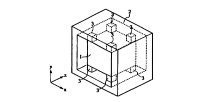
FIG. 1 is a perspective view showing the basic portion
of a multiiriode dielectric resonator device according to a
first embodiment.
FIG. 2 consists of cross sections showing the
electromagnetic field distributions in the respective modes
of the above resonator device.
FIG. 3 consists of cross sections showing the
electromagnetic field distributions in the respective modes
of the above resonator.
FIG. 4 consists of cross sections showing the
electromagnetic field distributions in the respective modes
of the above resonator device.
FIG. 5 is a perspective view showing the basic portion
of a multimode dielectric resonator device according to a
second embodiment.
FIG. 6 illustrates an example of a process of
manufacturing the above resonator device.
FIG. 7 is a graph showing the changes of the resonance
frequencies of the respective modes, occurring when the
sizes of the portions of the resonator device are changed.
FIG. 8 is a graph showing the changes of the resonance
frequencies of the respective modes, occurring when the
sizes of the portions of the resonator device are changed.
CA 02302951 2000-03-02
- 9 -
FIG. 9 is a perspective view showing the constitution
of the dielectric core portion of a multimode dielectric
resonator device according to a third embodiment.
FIG.' 10 is a graph showing the changes of the
resonance frequencies of the respective modes, occurring
when the depth of a groove of the above resonator device is
changed.
FIG. 11 is a perspective view showing a dielectric
core portion for use in description of the coupling means
for coupling the respective resonance modes of each of the
multimode resonator devices according to fourth to sixth
embodiments.
FIG. 12 illustrates examples of the electromagnetic
field distributions caused when the two TM modes of the
multimode dielectric resonator device according to a fourth
embodiment are coupled to each other.
FIG. 13 consists of perspective views showing examples
of the magnetic field distributions of the two resonance
modes of the above resonator device.
FIG. 14 illustrates the constitutions of coupling
holes for coupling the two resonance modes of the above
resonator device.
FIG. 15 illustrates electromagnetic distributions, and
the configurations of coupling-conditioning holes in a
multimode dielectric resonator device according to a fifth
CA 02302951 2000-03-02
- 1~ -
embodiment.
FIG. 16 illustrates the electromagnetic field
distributions of the respective modes in a multimode
dielectric resonator device according to the sixth
embodiment.
FIG. 17 illustrates the electromagnetic field
distributions of two modes in the cross sections of the a-a
portions shown in FIG. 16.
FIG. 18 illustrates the configuration of a coupling-
conditioning groove for the resonance modes in the first and
second stages shown in FIG. 16.
FIG. 19 illustrates the electric field distributions
in the cross sections of the b-b portions shown in FIG. 16.
FIG. 20 illustrates the configuration of a groove for
coupling the resonance modes in the second and third stages
shown in FIG. 16.
FIG. 21 illustrates the electric field distributions
in the cross sections of the a-a portions shown in FIG. 16.
FIG. 22 illustrates the configuration of a groove for
coupling-conditioning the resonance modes in the third and
fourth stages shown in FIG. 16.
FIG. 23 illustrates the electric field distributions
in the cross sections of the b-b portions shown in FIG. 16.
FIG. 24 illustrates the configuration of a groove for
coupling-conditioning the resonance modes in the fourth and
CA 02302951 2000-03-02
- 11 -
fifth stages shown in FIG. 16.
FIG. 25 consists of perspective views each showing an
example of the constitution of the major portion of the
multimode dielectric resonator device according to the
seventh embodiment.
FIG. 26 consists of partially exploded perspective
views each showing an example of the constitution of a
conventional dielectric resonator device.
FIG. 27 illustrates examples of the electromagnetic
field distributions in the conventional single mode
dielectric resonator;
FIG. 28 is a perspective view showing the basic
portion of a multimode dielectric resonator device according
to an eighth embodiment.
FIG. 29 consists of cross sections showing the
electromagnetic field distributions of the respective modes
in the above resonator device.
FIG. 30 consists of cross sections showing the
electromagnetic field distributions of the respective modes
in the above resonator device.
FIG. 31 consists of cross sections showing the
electromagnetic wave distributions of the respective modes
in the above resonator device.
FIG. 32 consists of graphs showing the relations
between the thickness of the dielectric core of the above
CA 02302951 2000-03-02
- 12 -
resonator device and the resonance frequencies of the
respective modes.
FIG. 33 illustrates the configuration of a dielectric
filter . '
FIG. 34 illustrates the configuration of another
dielectric filter.
FIG. 35 illustrates the configuration of a
transmission-reception shearing device.
FIG. 36 illustrates the configuration of a
communication device.
Best Mode for Carrying Out the Invention
The configuration of a multimode dielectric resonator
device according to a first embodiment will be described
with reference to FIGS. 1 to 4.
FIG. 1 is a perspective view showing the basic
constitution portion of the multimode dielectric resonator
device. In this figure, reference numerals 1, 2, and 3
designate a substantially parallelepiped-shaped dielectric
core, an angular pipe-shaped cavity, and supports for
supporting the dielectric core 1 substantially in the center
of the cavity 2. A conductor film is formed on the outer
peripheral surface of the cavity 2. On the two open-faces,
dielectric plates or metal plates each having a conductor
film formed thereon are disposed, respectively, so that a
CA 02302951 2000-03-02
- 13 -
substantially parallelepiped-shaped shield space is formed.
In addition, an open-face of the cavity 2 is opposed to an
open-face of another cavity so that the electromagnetic
fields In predetermined resonance modes are coupled to
provide a multistage.
Ordinarily, the supports 3 shown in FIG. 1, made of a
ceramic material having a lower. dielectric constant than the
dielectric core 1 are disposed between the dielectric core 1
and the inner walls of the cavity 2 and fired to be
integrated.
The resonance modes, caused by the dielectric core 1
shown in FIG. 1, are illustrated in FIGS. 2 to 4. In these
figures, x, y, and z represent the co-ordinate axes in the
three-dimensional directions shown in FIG. 1. FIGS. 2 to 4
show the cross-sections taken through the respective two-
dimensional planes. In FIGS. 2 to 4, a continuous line
arrow indicates an electric field vector, and a broken line
arrow indicates a magnetic field vector. The symbols "
and " x " represent the direction of an electric field and
that of a magnetic field, respectively. FIG. 2 to 4 show
only a total of six resonance modes, that is, the TMOlb
modes in the three directions, namely, the x, y, and z
directions, and the TEOlb modes in the same three directions
as described above. In practice, higher resonance modes
exist. In ordinary cases, these fundamental modes are used.
CA 02302951 2000-03-02
- 14 -
Next, the configuration of a multimode dielectric
resonator device according to a second embodiment will be
described with reference to FIGS. 5 to 8.
FIG. 5 is a perspective view showing the basic
constitution portion of a multimode resonator device. In
this ffigure, reference numerals 1, 2, and 3 designate a
substantially parallelepiped-shaped dielectric core, an
angular pipe-shaped cavity, and supports for supporting the
dielectric core 1 substantially in the center of the cavity
2. A conductor film is formed on the outer peripheral
surface of the cavity 2. In this example, two supports 3
are provided on each of the four inner walls of the cavity,
respectively. The other configuration is the same as that
in the first embodiment.
FIG. 6 shows an example of a process of producing the
multimode dielectric resonator device shown in FIG.5. First,
as shown in (A), the dielectric core 1 is molded integrally
with the cavity 2 in the state that the dielectric core 1
and the cavity 2 are connected by means of connecting parts
1'. Hereupon, molds for the molding are opened in the axial
direction of the cavity 2, through the open faces of the
angular pipe-shaped cavity 2. Subsequently, as shown in (B),
the supports 3 are temporarily bonded with a glass glaze in
paste state, adjacently to the connecting parts 1' and in
the places corresponding to the respective corner portions
CA 02302951 2000-03-02
- 15 -
of the dielectric core 1. Further, Ag paste is applied to
the outer peripheral surface of the cavity 2. Thereafter,
the supports 3 are baked to bond to the dielectric core 1
and'the inner walls of the cavity 2 (bonded with the glass
glaze), simultaneously when an electrode film is baked.
Thereafter, the connecting parts 1' are scraped off to
produce the structure in which.the dielectric~core 1 is
mounted in the center of the cavity 2 as shown in (C) of the
same figure. In this case, for the dielectric core 1 and
the cavity 2, a dielectric ceramic material of Zr02 - Sn02 -
Ti02 type with s r = 37 and tan b = 1/20,000 is used. For
the supports 3, a low dielectric constant dielectric ceramic
material of 2Mg0 - Si02 type with a r = 6 and tan b = 1/2,000
is used. Both have nearly equal liner expansion
coefficients. No excess stress is applied to the bonding
surfaces between the supports and the dielectric core or the
cavity, when the dielectric core is heated, and the
environmental temperature is changed.
In the above respective embodiments, a single support
is described as an example. The supports may be molded
integrally with the dielectric core or the cavity, or all of
the supports, the cavity, and the dielectric core may be
integrally molded.
FIG. 7 shows the changes of the resonance frequencies
of the TE018-x, TEOlb-y, and TEOls-z modes, occurring when
CA 02302951 2000-03-02
- 16 -
the thickness in the Z axial direction of the dielectric
core 1 and the cross sectional area of the supports 3, shown
in FIG. 5, are varied. As illustrated, with the thickness
in the z axial direction of the dielectric core being
increased, the resonance frequencies of the TE018-x and
TE018-y modes are more reduced. Further, as the cross
sectional area of each support.is increased, the resonance
frequency of the TE018-z mode is reduced more considerably.
By designing appropriately the thickness in the z axial
direction of the dielectric core 1 and the cross sectional
area of each support 3 by utilization of these relations,
the resonance frequencies of the three modes of TE018-x,
TE018-y, and TEOls-z can be made coincident with each other.
Thus, by coupling predetermined resonance modes to each
other, the multistage can be realized.
FIG. 8 shows the changes of the resonance frequencies
of the above-described three TM modes, occurring when the
wall thickness of the cavity 2, the thickness in the Z axial
direction of the dielectric core 1 and the cross sectional
area of the supports 3, shown in FIG. 5, are varied. When
only the wall thickness of the cavity is thickened, the
resonance frequencies of the TMO1S-x and TMOlb-y modes are
reduced more considerably as compared with the resonance
frequency of the TMO1S-z mode. When the thickness in the z
axial direction of the dielectric core is thickened, the
CA 02302951 2000-03-02
- 17 -
resonance frequency of the TM018-z mode is reduced more
considerably as compared with the resonance frequencies of
the TM018-x, TM018-y modes. When the cross sectional area of
each support is increased, the resonance frequencies of the
TM018-x, TM018-y modes are reduced more considerably as
compared with the resonance frequency of the TM018-z mode.
By utilization of these relations, the resonance frequencies
of the three modes can be made coincident with each other at
characteristic points, designated by p1 and p2 in the figure,
for example.
FIG. 9 is a perspective view showing the configuration
of the dielectric core portion of a multimode dielectric
resonator device according to a third embodiment. As
already described with reference to FIGS. 2 to 4, in the
TE018 modes, the electric field components are concentrated
onto the vicinity of the respective cross sections which
divide the dielectric core into eight portions. On the
other hand, such concentration doesn't occur in the TM018
modes, and therefore, as shown in FIG.9, by forming a cross-
shaped groove in each of the faces of the dielectric core,
each groove crossing at the center of the face, the
resonance frequencies of the TE018 modes can be selectively
increased.
FIG. 10 is a graph showing the relations between the
groove depth and the changes of the resonance frequencies of
CA 02302951 2000-03-02
- 18 -
the both modes. When no groove is provided, generally, the
resonance frequency of the TEOls mode is lower than that of
the TM018 mode. In the case where the grooves g are provided,
with the depth being deeper, the'resonance frequency of the
TMO1S mode is increased, and at a point, becomes coincident
with the resonance frequency of the TE018 mode. Further, in
the case where the groove depth is constant, and the groove
width is widened, the resonance frequency of the TE018 mode
can be selectively increased with the groove width being
wider. In the case where the resonance frequency of the
TE018 mode is lower than that of TM018 mode, caused by the
respective sizes of the dielectric core, the cavity, and the
supports, and the relative dielectric constants of
respective portions, and so forth, without the above grooves
being provided, the resonance frequency of the TEO1S mode
and that of the TMOlb mode can be coincident with each other
by forming the grooves in the dielectric core as described
above. By making the resonance frequencies of the both
modes coincident with each other, and coupling the both
modes, a multistage can be realized.
Next, the configuration of a multimode dielectric
resonator device in which the TMOlb modes are coupled to
each other will be described with reference to FIGS. 11 to
14.
FIG. 11 is a perspective view showing a dielectric
CA 02302951 2000-03-02
- 19 -
core portion. In the figure, reference numerals h0 to h4
designate holes for use in adjusting the coupling
coefficient obtained between predetermined modes.
FIG. 12 illustrates the electromagnetic field
distributions of the respective modes. Hereupon, a
continuous line arrow indicates an electric field, and a
broken line does a magnetic field. In (A) illustrated are
the electromagnetic distributions of two main modes to be
coupled, that is, the TM018-(x-y) mode and the TM018-(x+y)
mode, respectively. In (B), illustrated are the
electromagnetic distributions of an odd mode and an even
mode which are the coupled modes. In this example, the odd
mode can be expressed by a TM018-y mode, and the even mode
by a TM018-x mode.
FIG. 13 consists of perspective views showing the
magnetic field distributions of the above main modes,
respectively. When the resonance frequency of the odd mode
is represented by fo, and that of the even mode by fe, the
coupling coefficient k12 of the two mode is expressed by the
following formula.
k12 « 2 (fo - fe)/(fo + fe)
Accordingly, the main modes, that is, the TMOlb-(x-y)
mode and the TM018-(x+y) mode are coupled by providing a
difference between the fo and fe. Accordingly, as shown in
FIG. 14, a hole ho lying in the center of the dielectric
CA 02302951 2000-03-02
- 20 -
core is elongated in the y axial direction. That is, by
forming a groove elongating in parallel to the direction of
the electric field of TM018-y and perpendicularly to the
direction of the electric: field of TM018-x, the relation of
fe > fo is obtained. On the contrary, by elongating the hole
ho in the axial direction, the relation of fe < fo is
obtained. In either case, coup~.ing can be achieved at a
coupling coefficient corresponding to the fo and fe.
In the above example, the TMO1S-(x-y) mode and the
TMO1S-(x+y) mode are main modes, and the TMO1S-y mode and the
TM018-x mode are coupled modes. On the contrary, the TM018-
y mode and the TM018-x mode may be main modes, and the
TM018-(x-y) mode and the TM018-(x+y) mode may be coupled
modes. In this case, the inner diameter of the hole ho
shown in FIG. 14 may be lengthened in a diagonal direction.
FIG. 15 illustrates that a TM mode and a TE mode are
coupled to each other, and particularly, three modes are
sequentially coupled to each other, as an example. The
configuration of the dielectric core is the same as that
shown in FIG. 11. In FIG. 15, in (A), illustrated are the
electromagnetic field distributions of the three modes, that
is, the TM018-(x-y), TE018=z, and TMOlb-(x+y) modes,
respectively. A continuous line arrow indicates an electric
field, and a broken line a magnetic field. In (B),
illustrated are the coupling relations between the above-
CA 02302951 2000-03-02
- 21 -
described TE mode and the other two TM modes. The figure
presented in the left-hand side of (B) shows the electric
distribution of the TMO1S-(x-y) mode, and that of the TEO1S-z
mode which overlap each other. By breaking the balance df
the electric field strengths at points A and B, energy is
transferred from the TMO1S-(x-y) mode to the TEOlb-z mode.
Accordingly, as shown in the figure presented~in the left
hand side of (C) of the same figure, the coupling
coefficient k12 is adjusted by widening the inner diameter
of a hole h2 to provide a difference between the hole h2 and
a hole hl.
Similarly, the figure presented in the right-hand side
of (B) shows the electric distributions of the TE018-z mode,
and that of the TMOlb-(x+y) mode which overlap each other.
In this case, by breaking the balance of the electric field
strengths at points C and D, energy is transferred from the
TE018-z mode to the TM018-(x+y) mode. Accordingly, as shown
in the figure presented in the right-hand side of (C) of the
same figure, the coupling coefficient k 23 is adjusted by
widening the inner diameter of a hole h4 to provide a
difference between the hole h4 and a hole h3.
FIG. 16 illustrates an example of coupling five
resonance modes sequentially, which is operated as a five
stage resonator, as an example. The configuration of the
dielectric core is the same as that shown in FIG. 11. In
CA 02302951 2000-03-02
- 22 -
FIG. 16, a continuous line indicates an electric field
distribution, and a broken line a magnetic field
distribution.
First, the coupling of TM018-(x-y) and TEOls-(x+y)'will
be discussed. FIG. 17 illustrates the electromagnetic field
distributions of the above two modes in the cross sections
taken through the a-a portion in FIG. 16. In.(B),
illustrated are the electromagnetic field distributions of
the two modes which overlap each other. By breaking the
balance of the electric field strengths of the TM018-(x-y)
and the TE018-(x+y) in the a-a cross section, energy is
transferred from the TM018-(x-y) mode to the TE018-(x+y) mode.
Accordingly, as shown in FIG. 18, the size of the hole is
made different at the upper side and the underside in the a-
a cross section. In the example shown in this figure, a
groove g elongating in the (x + y) axial direction is
provided in the upper side of the dielectric core 1
Next, the coupling of the TE018-(x+y) mode and the
TE018-z mode will be discussed. FIG. 19 (A) illustrates the
electric field distributions of the above-described two
modes in the cross section of the b-b portion of the
dielectric core. Further, in (B), illustrated are the
electric field distributions of an even mode and an odd mode
which are the coupled modes. When the above-described two
modes are coupled to each other, it is suggested that a
CA 02302951 2000-03-02
- 23 -
difference is given between the resonance frequency fe of
the even mode and that of the odd mode. For this purpose,
as shown in FIG. 20, the symmetry of the cross section of
the b-b portion with respect to the diagonal direction'is
broken. In this example, grooves g are formed in the
vicinity of the open-portion at the upper side of a hole h2
and that of the open-end at the underside of a hole hl,
respectively. Thereby, the resonance frequency fe of the
even mode shown in FIG. 19 (B) becomes higher than the
resonance frequency fo of the odd mode. The TE018-(x+y) and
the TEO1S-z mode are coupled at a coupling coefficient
corresponding to the difference.
Next, the coupling of the third stage and the fourth
stage shown in FIG. 16, that is, the coupling of the TE018-z
mode and the TE018-(x-y) mode will be discussed. FIG. 21
illustrates the electric field distributions of the above-
described two modes in the cross section of the a-a portion
of the dielectric core. In (B), illustrated are the
electric field distributions of an even mode and an odd mode,
which are the coupled modes. When the above-described two
modes are coupled, it is suggested that a difference is
given between the resonance frequency fe of the even mode
and the resonance frequency of the odd mode. For this
purpose, as shown in FIG. 22, the symmetry of the cross
section of the a-a portion with respect to the diagonal
CA 02302951 2000-03-02
- 24 -
direction is broken. In this example, grooves g are formed
in the vicinity of the open-portion at the upper side of a
hole h3 and that of the open-end at the underside of a hole
h4, respectively. Thereby, the resonance frequency fo of
the odd mode shown in FIG. 21 (B) becomes higher than the
resonance frequency fe of the even mode. The TEOlb-z and the
TEOlb-(x-y) mode are coupled at.a coupling coefficient
corresponding to the difference.
Next, the coupling of TE018-(x-y) and TM018-(x+y) shown
in FIG. 16 will be discussed. FIG. 23 (A) illustrates the
electromagnetic field distributions of the above two modes
in the cross sections of the b-b portion in FIG. 16. In (B),
illustrated are the electromagnetic field distributions of
the two modes which overlap each other. By breaking the
balance of the electric field strengths of the TE018-(x-y)
and the TM018-(x+y) in the b-b cross section, as described
above, energy is transferred from the TE018-(x-y) mode to
the TM018-(x+y) mode. Accordingly, as shown in FIG. 24, the
sizes of the hole at the upper side and the underside in the
b-b cross section are made different. In the example shown
in this figure, a groove g elongating in the (x - y) axial
direction in the upper side of the dielectric core 1 is
provided.
In the above-described embodiment, coupling means for
coupling the respective resonance modes of the dielectric
CA 02302951 2000-03-02
- 25 -
core to an external circuit is not illustrated. For example,
if a coupling loop is used, an external coupling may be
achieved by disposing the coupling loop in the direction
where the magnetic filed of a mode to be coupled passes as
described later.
In the above described examples, plural resonance
modes are sequentially coupled. However, an example of
using the plural resonance modes independently, not coupling
the respective resonance modes to each other, will be
described with reference to FIG. 25 below.
In FIG. 25, a long and two short dashes line indicates
a cavity where a dielectric core 1 is disposed. The
supporting structure for the dielectric core 1 is omitted.
An example of forming a band rejection filter is illustrated
in (A) of this figure. Reference numerals 4a, 4b, and 4c
each represent a coupling loop. The coupling loop 4a is
coupled to a magnetic field (magnetic field of the TM018-x
mode) in a plane parallel to the y - z plane, the coupling
loop 4b is coupled to a magnetic field (magnetic field of
the TM018-y mode) in a plane parallel to the x - z plane,
and the coupling loop 4c is coupled to a magnetic field
(magnetic field of the TM018-z mode) in a plane parallel to
the x - y plane. One end of each of these coupling loops 4a,
4b, and 4c is grounded. The other ends of the coupling
loops 4a and 4b, and also, the other ends of the coupling
CA 02302951 2000-03-02
- 26 -
loops 4b and 4c are connected to each other through
transmission lines 5, 5 each having an electrical length
which is equal to ~,/4 or is odd-number times of ~,/4,
respectively. The other ends of the coupling loops 4a, 4c
are used as signal input-output terminals. By this
configuration, a band rejection filter is obtained in which
adjacent resonators of the three resonators are connected to
a line with a phase difference of ~c/2.
Similarly, a band pass filter may be formed by
coupling predetermined resonance modes through a coupling
loop, and a transmission line, if necessary.
FIG. 25 (B) illustrates an example of forming a
synthesizer or distributor. Hereupon, reference numerals 4a,
4b, 4c, and 4d designate coupling loops. The coupling loop
4a is coupled to a magnetic field (magnetic field of the
TMO1S-x mode) in a plane parallel to the y - z plane. The
coupling loop 4b is coupled to a magnetic field (magnetic
field of the TM018-y mode) in a plane parallel to the x - z
plane. The coupling loop 4c is coupled to a magnetic filed
(magnetic field in the TMO1S-z mode) in a plane parallel to
the x - y plane. Regarding the coupling loop 4d, the loop
plane is inclined to any of the y - z plane, the x - z plane,
and the x - y plane, and coupled to the magnetic fields of
the above three modes, respectively. One ends of these
coupling loops are grounded, respectively, and the other
CA 02302951 2000-03-02
- 27 -
ends are used as signal input or output term~.nals. In
particular, when the device is used as a synthesizer, a
signal is input through the coupling loops 4a, 4b, and 4c,
and outputs from the coupling loop 4d. When the'device is
used as a distributor, a signal is input through the
coupling loop 4d, and output from the coupling loops 4a, 4b,
and 4c. Accordingly, a synthesizer with three inputs and
one output or a distributor with one input and three outputs
are obtained.
In the above example, the three resonance modes are
utilized, independently. At least four modes may be
utilized. Further, a composite filter in which a band-pass
filter and a band- rejection filter are combined can be
formed by coupling some of the plural resonance modes
sequentially to form the band-pass filter, and making the
other resonance modes independent to form the band-rejection
filter.
Next, an example of a triplex mode dielectric
resonator device will be described with reference to FIGS.
28 to 32.
FIG. 28 is a perspective view showing the basic
constitution portion of a triplex mode dielectric resonator
device. In this figure,,reference numeral 1 designates a
square plate-shaped dielectric core of which two sides have
substantially equal lengths, and the other one side is
CA 02302951 2000-03-02
- 28 -
shorter than each of the two sides. The reference numerals
2 and 3 designate an angular pipe-shaped cavity and a
support for supporting a dielectric core 2 substantially in
the center of the cavity 2, respectively. A conductor film
is formed on the outer peripheral surface of the cavity 2.
Dielectric sheets each having a conductor film formed
thereon or metal sheets are disposed on the two open faces
to constitute a substantially parallelepiped-shaped shield
space. Further, an open- end of another cavity is opposed
to an open-face of the cavity 2, so that electromagnetic
fields in predetermined resonance modes are coupled to each
other to realize a multi-stage.
The supports 3 shown in FIG. 28, made of a ceramic
material having a lower dielectric constant than the
dielectric core 1, are disposed between the dielectric core
1 and the inner walls of the cavity 2, respectively, and
fired to be integrated.
FIGS. 29 to 31 show the resonance modes caused by the
dielectric core 1 shown in FIG. 28. In these figures, x, y,
and z represent the co-ordinate axes in the three
dimensional directions shown in FIG. 28. FIGS. 29 to 31
show the cross sectional views taken through the two-
dimensional planes, respectively. In FIGS. 29 to 31, a
continuous line arrow designates an electric field vector, a
broken line arrow does a magnetic field vector, and symbols
CA 02302951 2000-03-02
- 29 -
and "x" do the directions of the electric field and the
magnetic field, respectively. In FIGS. 29 to 31, shown are
the TEOlb mode (TE018-y mode) in the y-direction, the TMO1S
mode (TMOlb-x) in the x-direction, and th'e TM018 mode (TM018-
z) in the z-direction.
FIG. 32 shows the relations between the thickness of
the dielectric core and the resonance frequencies of the six
modes. In (A), the resonance frequency is plotted as
ordinate. In (B), the resonance frequency ratio based on
the TM018-x mode is plotted as ordinate. In (A) and (B), the
thickness of the dielectric core, expressed as oblateness,
is plotted as abscissa. The TE018-z mode and the TE018-x
mode are symmetric. White triangle marks representing the
TE018-z mode and black triangle marks for the TEOlb-x mode
overlap each other. Similarly, the TMOlb-z mode and the
TM018-x mode are symmetric. White circle marks representing
the TMOls-z mode, and black circle marks for the TM018-x
mode overlap each other.
Like this, as the thickness of the dielectric core is
thinned (the oblateness is decreased), the resonance
frequencies of the TE018-y mode, the TMO1S-x mode, and the
TMO1S-z mode have a larger difference from those of the
TMO1S-y mode, the TE018-x, and the TE018-z mode, respectively.
In this embodiment, the thickness of the dielectric
core is set by utilization of the above-described relation,
CA 02302951 2000-03-02
- 30 -
and the TE018-y, TM018-x, and TMOlb-z modes are used. The
frequencies of the other modes, that is, the TM018-y, TE018-
x, and TEO1S-z modes are set to be further separated from
those of the above-described modes sb as not to be affected
by them, respectively.
Next, an example of a dielectric filter including the
above-described triplex mode dielectric resonator device
will be described with reference to FIG. 33. In FIG. 33,
reference numerals la, 1d designate prism-shaped dielectric
cores, and are used as a TM single mode dielectric resonator.
Reference numerals 1b, lc designate square plate-shaped
dielectric cores in which two sides have a substantially
equal length, and the other one side is shorter than each of
the two sides, respectively, and are used as the above
triplex mode dielectric resonator. The triplex mode
consists of three modes, that is, the TM018-(x-y) mode, the
TE018-z mode, and the TM018-(x+y) mode, respectively,~as
shown in FIG. 15.
Reference numerals 4a to 4e each represent a coupling
loop. One end of the coupling loop 4a is connected to a
cavity 2, and the other end is connected to the core
conductor of a coaxial connector (not illustrated), for
example. The coupling loop 4a is arranged in the direction
where a TM single mode magnetic field (magnetic force line)
caused by the dielectric core la passes the loop plane of
CA 02302951 2000-03-02
- 31 -
the coupling loop 4a, so that the coupling loop 4a is
magnetic-field coupled to the TM single mode caused by the
dielectric core la. The vicinity of one end of the coupling
'loop 4b is elongated in the direction where it is magnetic-
field coupled to the TM single mode of the magnetic core la,
while the other end is elongated in the direction where it
is magnetic-field coupled to the TM018-(x-y) mode of the
dielectric core 1b. Both ends of the coupling loop 4b are
connected to the cavity 2. The vicinity of one end of the
coupling loop 4b is elongated in the direction where it is
magnetic-field coupled to the TM single mode of the magnetic
core la, while the other end thereof is elongated in the
direction where it is magnetic field coupled to the TM018-
(x-y) mode of the dielectric core 1b. Both ends of the
coupling loop 4b are connected to the cavity 2. The
vicinity of one end of the coupling loop 4c is elongated in
the direction where it is magnetic- field coupled to the
TMO18-(x+y) mode of the magnetic core la, while the other
end thereof is elongated in the direction where it is
magnetic-field coupled to the TM018-(x-y) mode of the
dielectric core 1b. Both ends of the coupling loop 4c are
connected to the cavity 2. Further, one end of the coupling
loop 4d is elongated in the direction where it is magnetic-
field coupled to the TM018-(x+y) mode of the magnetic core
lc, while the other end thereof is elongated in the
CA 02302951 2000-03-02
- 32 -
direction where it is magnetic-field coupled to the TM
single mode of the dielectric core 1d. Hoth ends of the
coupling loop 4d are connected to the cavity 2. The
' coupling loop 4e is arranged in 'the direction where it is
magnetic-field coupled to the TM single mode of the magnetic
core 1d. One end of the coupling loop 4e is connected to a
cavity 2, while the other end is connected to. the core
conductor of a coaxial connector (not illustrated).
Coupling-conditioning holes h2 and h4 are formed in
the triplex mode dielectric resonator caused by the
dielectric core 1b, and the triplex mode dielectric
resonator caused by the dielectric core 1c, respectively.
As shown in FIG. 15, with the coupling conditioning hole h2,
energy is transferred from the TM018-(x-z) mode to the TE018-
y mode. With the coupling-conditioning hole h4, energy is
transferred from the TEOlb-z mode to the TM018-(x+y) mode.
Thereby, the dielectric cores 1b, lc form resonator circuits
in which three stage resonators are longitudinally connected,
respectively, and operate as a dielectric filter comprising
eight stage resonators (1 + 3 + 3 + 1) longitudinally
connected to each other, as a whole.
Next, an example of another dielectric filter
including the above-described triplex mode dielectric
resonator device will be described with reference to FIG. 34.
In the example shown in FIG. 33, the coupling loops, which
r CA 02302951 2000-03-02
- 33 -
are coupled to the respective resonance modes caused by
adjacent dielectric cores, are provided. However, each
dielectric resonator device may be provided for each
dielectric core, independently. In FIG. 34, reference
numerals 6a, 6b, 6c, and 6d designate dielectric resonator
devices, respectively. These correspond to the resonators
which are caused by the respective dielectric~cores shown in
FIG. 33 and are separated from each other. The dielectric
resonator devices are positioned as distantly from each
other as possible so that two coupling loops provided for
the respective dielectric resonator devices are prevented
from interfering with each other. Reference numerals 4a,
4b1, 4b2, 4c1, 4c2, 4d1, 4d2, and 4e designate respective
coupling loops. One end of each of the coupling loops is
grounded inside of the cavity, and the other end is
connected to the core conductor of a coaxial cable by
soldering or caulking. The outer conductor of the coaxial
cable is connected to the cavity by soldering or the like.
Regarding the dielectric resonator 6d, the figure showing
the coupling loop d2 and the figure showing the coupling
loop 4e are separately presented for simple illustration.
The coupling loops 4a, 4b1 are coupled to the
dielectric core la, respectively. The coupling loop 4b2 is
coupled to the TM018-(x-z) of the dielectric core 1b. The
coupling loop 4c1 is coupled to the TMOls-(x+z) of the
CA 02302951 2000-03-02
- 34 -
dielectric core 1b. Similarly, the coupling loop 4c2 is
coupled to the TM018-(x-z) of the dielectric core lc. The
coupling loop 4d1 is coupled to the TMOls-(x+z) of the
dielectric core lc. The coupling loops 4d2 and 4e are '
coupled to the dielectric core 1d, respectively.
Accordingly, the coupling loops 4b1 and 4b2 are
connected through a coaxial cable, the coupling loops 4c1
and 4c2 are connected through a coaxial cable, and further
the coupling loops 4d1 and 4d2 are connected through a
coaxial cable, and thereby, the device operates as a
dielectric filter comprising the resonators in eight stages
(1 + 3 + 3 + 1) longitudinally connected to each other, as a
whole, similarly to that shown in FIG. 34.
Next, an example of the configuration of a
transmission - reception shearing device will be shown in
FIG. 35. Hereupon, a transmission filter and a reception
filter are band-pass filters each comprising the above
dielectric filter. The transmission filter passes the
frequency of a transmission signal, and the reception filter
passes the frequency of a reception signal. The connection
position at which the output port of the transmission filter
and the input port of the reception filter are connected is
such that it has the relation that the electrical length
between the connection point and the equivalent short-
circuit plane of the resonator in the final stage of the
CA 02302951 2000-03-02
- 35 -
transmission filter is odd-number times of the 1/4 wave
length of the wave with a reception signal frequency, and
the electrical length between the above-described connection
point and the equivalent' short-circuit plane of the
resonator in the first stage of the reception filter of the-
reception filter is odd-number times of the 1/4 wavelength
of a wave with a transmission signal frequency.. Thereby,
the transmission signal and the reception signal can be
securely branched.
As seen in the above-description, similarly, by
disposing plural dielectric filters between a port for use
in common and individual ports, a diplexer or a multiplexer
can be formed.
FIG. 36 is a block diagram showing the configuration
of a communication device including the above-described
transmission - reception shearing device (duplexer). The
high frequency section of the communication device is formed
by connecting a transmission circuit to the input port of a
transmission filter, connecting a reception circuit to the
output port of a reception filter, and connecting an antenna
to the input- output port of the duplexer.
Further, a communication device small in size, having
a high efficiency can be formed by use of circuit components
such as the duplexer, the multiplexer, the synthesizer, the
distributor each described above, and the like which are
CA 02302951 2000-03-02
- 36 -
formed of the multimode dielectric resonator devices.
As seen in the above-description, according to the
present invention defined in claims 1, 2, the dielectric
core having a substantial parallelepiped-shape is disposed
substantially in the center of the cavity having a
substantial parallelepiped-shape. Therefore, the
concentration degree of an electromagnetic field energy onto
the dielectric core, though it is in a TM mode, is enhanced,
a real electric current flowing through the cavity becomes
fine, and the Qo can be enhanced. Moreover, though the
dielectric core and the cavity are single, respectively, the
miniaturization as a whole can be achieved.
According to the present invention defined in claims 3
and 4, the multiplexing, that is, duplexing or triplexing
can be made, so that the miniaturization as a whole can be
realized.
According to the preset invention defined in claim 5,
a dielectric resonator device using both modes, namely, a TM
mode and a TE mode can be obtained. The dielectric
resonator device has a multimode, that is, a quadruplex mode
or higher, so that further miniaturization as a whole can be
realized.
When the above-described respective multiplexed
resonance modes are used independently, not coupled to each
other, for example, a circuit comprising plural resonators,
CA 02302951 2000-03-02
- 37 -
such as a band-rejection filter, a synthesizer, a
distributor, or the like, can be formed so as to be small in
size by use of a single dielectric core.
According to 'the present invention defined in clailin 6,
a resonator device comprising plural dielectric resonators
connected into a multistage is formed. A small-sized
dielectric resonator device having a band-pass filter
characteristic can be obtained. By use of a resonator in
which some of the plural resonance modes are sequentially
coupled, and the other resonance modes are uses as an
independent resonator, respectively, a filter in which a
band-pass filter and a band-rejection filter are combined
can be formed.
According to the present invention defined in claim 7,
a dielectric filter having a high Q filter characteristic
and a small-size can be obtained.
According to the present invention defined in claim 8,
a composite dielectric filter small in size, having a low
loss can be obtained.
According to the present invention defined in claim 9,
a synthesizer small in size, having a low loss can be
obtained.
According to the present invention defined in claim 10,
a distributor small in size, having a low loss can be
obtained.
CA 02302951 2000-03-02
- 38 -
According to the present invention defined in claim 11,.
a communication device small in size, having a high
efficiency can be obtained.
Industrial Applicability
As seen in the above-description, the dielectric
resonator device, the dielectric filter, the composite
dielectric filter, the distributor, and the communication
device including the same, according to the present
invention, each of which operates in a multimode can be used
in a wide variety of electronic apparatuses, for example, in
the base stations of a mobile communication system.