Note: Descriptions are shown in the official language in which they were submitted.
CA 02303324 2000-03-08
WO 99/13576 PGT/US98/1446Z
METHOD AND APPARATUS FOR ENCODING
AND DECODING A BIT SEQUENCE
FOR TRANSMISSION OVER
POTS WIRING
FIELD OF THE INVENTION
The present invention relates generally to the field of encoding and decoding
digital data for transmission over a medium. More specifically, the present
invention relates to the decoding and encoding of a bit sequence for
transmission
over Plain Old Telephone Service (POTS) wiring.
BACKGROUND
Local Area Network (LAN) standards and products have not significantly
penetrated the home computing market for a number of reasons, including the
lack
of perceived need and the required installation of special cabling, which is
difficult
within a residential household. As multiple personal computers (PCs) are
becoming
increasingly common within households, the notion of implementing a LAN within
a residential environment is gaining in popularity. Specificaliy, the ability
to share
information between multiple PCs, and to share resources such as printers and
modems, is becoming increasingly attractive to home computer users. In
particular,
the ability to achieve shared, high-speed Internet access by a number of
computers
within a household is becoming important as multiple users within a residence
may
wish simultaneously to access the Internet.
One econonucal method of creating a LAN within a residential household
proposes using the existing telephone wiring within the residence (POTS
wiring} as
the medium over which the LAN is implemented. Such wiring typically comprises
unshielded, twisted-pair (UTP) telephone cable and may comprise either
Category 1
or Category 2 cable, as defined by the EIA/TIA 568 specification. The use of
such
residential telephone wiring poses a number of problems in that the
transmission of
data signals must occur over an arbitrary, unterminated wiring system, with
unknown electrical characteristics. This results in impedance mismatches and
the
lack of termination contributes to the persistent reflection of signals and
1't.~u7~sy 15:03 F.i1 70J 3OS 4785 CA 02303324 2000-03-08
-- .-~-.--. - -.- ---. ---. C~I 0 0 8
DEC 07 '99 11'07RM
°v1~ :1 a io'~t.' ~: SJ .~ ~ ~. 4'
'' ~ ~ ~~ ~ ° R 1999
reflection of signals and unpredictable peaks and valleys in frequency
response
within a band of interest. The power splitting effect of star configurations,
which
are commonly implemented in residential wiring, attenuate the levels of signal
features whose duration is short compared to the propagation delay of the wire
branches.
A LAN implemented over residential telephone wiring may also be
required to coexist with the POTS service, and must be FCC part 68 compliant,
which dictates the use of signals with no frequency components below 270 kHz
and transport levels below 178 mV.
SUMMARY OF THE INVENTION
According to a first aspect of invention, there is provided a method of
encoding a bit sequence as a symbol for transmission over a carrier medium.
The
symbol has a time duration indicative of the bit sequence, the time duration
of the
symbol being determined by first and second delimiters. The method commences
with the reception of the bit sequence at an encoder, whereafter a symbol,
having a
duration indicative of the bit sequence, is identificd_ This symbol includes
encoding and buffer portions. The buffer symbol portion is of sufficient time
duration to allow reflecrions, generated by the first delimiter on the caizier
medium, to decay to a predetermined level before propagation of the second
delimiter. In one embodiment, the first and second delimiters may be
respective
electrical pulses, and at least one bit of the bit sequence may be encoded
utilizing
the polarity of the second delimiter.
According to a second aspect of the invention, there is provided a method
of decoding a symbol having a time duration indicative of a bit sequence, the
time
duration be determined by first and second delimiters. The decoding method
commences when the first delimiter is detected, whereafter a timer is
initiated.
Detection of the second delimiter is blocked for a predetermined buffer
portion of
the symbol to prevent detection of reflections resulting from the propagation
of
the first delimiter over the carrier medium. The second delimiter is then
detected
after expiration of the buffer portion of the symbol. In one embodiment, at
least
one bit of the bit sequence may be decoded utilizing the polarity of the
second
delimiter.
2
,....
ABED ~
i
1~% 07199 15:09 F.~I 70J J08 :1785 CA 02303324 2000-03-08
_- ' - __-.-.--- -- - .-. -- - 11009
DE ~~
~'"~~-~ -~' n~~ 1999
The invention extends to an~ encoder and a decoder which implement the above
methodologies.
Other features of the present invention will be apparent from the accompanying
drawings and from the detailed description which follows.
BRIEF DESCRIPTION OF THE DRAWINGS
The present invention is illustrated by way of example and not limitation in
the
figures of the accompanying drawings, in which like references indicate
similar
elements and in which:
Figures la and lb illustrate Local Area Networks (L.A.Ns) implemented using
arbitrary topology TOPS wiring.
Figure 2 is a diagrammatic representation of a network station according to
one
embodiment of the present invention.
Figure 3 is a diagrammatic representation of a modem, according to one
embodiment of the present invention, included within the network station shown
in
Figure 2.
Figure 4 is a diagrammatic representation of a lObaseT-to-POTS adapter,
according to one embodiment of the present invention.
Figure S illustrates a sequence of symbols, each encoding a bit sequence and
constructed according to the teachings of the present invention.
Figure 6 is a coding tree illustrating a method, according to one embodiment
of
the present invention, of coding a bit sequence.
Figure 7 illustrates a waveform generated on POTS wiring by the application of
a pulse thereto.
Figures 8a and 8b provide a schematic illustration of an exemplary embodiment
of the modem shown in Figure 3.
Figures 9a and 9b are schematic illustrations of an encoder and a decodes
included within the modem shown in Figures 8a and 8b_
A>~tOED
1=,'07199 15:09 F..~ 703 X08 1785 CA 02303324 2000-03-08
_ - .- -. .-. -. .-- --. - - -. . ~ O 10
DEC 07 '99 ~11 07R
'v
os ~S.7li 6~~
DETAILED DESCRIPTION
A method and apparatus for encoding, and decoding, a bit sequence for
transmission of POTS witzng are described. In the following description, for
the
purposes of explanation, numerous specific details are set forth in order to
provide
a thorough understanding of the present invention_ It will be evident,
however, to
one skilled in the art that the present invention may be practiced without
these
specific details.
Apparatus - Overview
Figures 1a and lb each illustrate a respective Local Area Network (LAN)
and 12 which may be implemented utilizing arbitrary topology POTS wiring
14, such as UTP wiring, within a residential building I6. The wiring 14 fans
out
from a central connection point 18, through which the wiring 14 connected to a
central office, to numerous phone jacks 20 located throughout the building 16.
A
number of LAN devices (also termed "stations" or "nodes"), such as computers
22, modems 24 or printers 26, may be coupled to the wiring 14 via the jacks
20.
Regular telephones 28 are also shown to be coupled to the wiring 14 via
respective jacks 20. A number of branches of the wiring 14 may furthermore
terminate in a jack 20 into which a LAN device or telephone is not connected,
and
are accordingly unterminated. As will be appreciated from Figure 1a, the
wiring
14 interconnecting the LAN devices has an irregular topology, and includes a
number of unterminated branches. Impedance mismatches, the arbitrary topology,
and the lack of termination within the LANs 10 and 12 result in the reflection
of
signals and unpredictable frequency responses within these LANs 10 and 12.
Further, the star configuration illustrated in Figure la serves to attenuate
the
levels of signal features whose duration is short compared to the propagation
delay of the wire branches.
Turning now to Figure 2, there is illustrated a network station 30 coupled
to a LAN via uneharacterizcd, arbitrary topology wiring, such as the POTS
wiring
14 illustrated in Figures la and b. The network station 30 allows a number of
well-known protocol and LAN features to be implemented within the LANs 10
and 12. For example, the LAN 12 may use Ethernet, BISYNC or HI7LC framing,
4
1'G~u7/yy l5:oy F:~ 703 308 47gg CA 02303324 2000-03-08
_- --. ~ -. --- -----__---------- l~ 011
DEC 07,'99-. 11:07RM
'~ ~t
~'7~;, add
~~r~ ,~. ~' P R 1999
and implement Collision Detecting, Collision Avoiding, TDMA, Polled or Token
Passing access methods.
An overview of the various components of the network station 30 will now
be provided. The station 30 comprises a network device 36 and an adapter 35.
The adapter 35 includes a modem 32 that serves to adapt a communications
controller 34 (such as an ethernet communications controller) of the network
device 36 (such as a computer) for communication over the arbitrary POTS
wiring
14. In one embodiment, the modem 32 provides medium interface, signal
encoding and decoding (ENDEC), clock recovery and collision detection
functions. Exemplary embodiments of collision detection circuitry and
functions
that may be implemented within the adapter 35 are described in co-pending
application Serial No. 08/925,043 entitled "METHOD AND APPARATUS FOR
DETECTII'TG COLLISIONS ON A NETWORK", filed 08 September 1997, and
assigned to the assignee of this application. To accommodate a variable bit
rate
encoding/decoding scheme, and to control the flow the data between the network
device 36 and the wiring 14, the modem 32 controls the clocking of data to and
from the communications controller 34. The modem 32 may further support
Carrier Sense Multiple Access/Collision Detection (CSMA/CD) based Media
Access Control (MAC) layers and accordingly provides carrier detect and
collision indication signals. The modem 32 is furthermore shown to be coupled
to
a microprocessor system 38 of the network device 36 via a management
interface,
which allows the modem 32 to be controlled by software executing within the
microprocessor system 38. The adapter 35 further incorporates a coupler module
40 by which the network station 30 is coupled to the jack 20 and POTS wiring
I4.
The coupler module 40 includes a pair of RJ-11 ports through which the wall
jack
20 and the telephone 28 are coupled to the network device 36. The coupler
module 40 is furthermore connected to the modem 32 via a transmit/reccive
connection 42.
A filter (not shown) is incorporated within the coupler module 40, and acts
as a bandpass with a lower cutoff frequency of around 400 kHz and upper cutoff
frequency around 4 Mhz. The filter is AC coupled to the wiring 14 to prevent
S
12;07199 15:10 F:~ 703 308 4755 CA 02303324 2000-03-08
----- ---- ---- - ~ 012
t 9~ ,~:1 40 ~AhU
. . ~~iE~l$~_ ~ ~ n ~ ~ - lg~~
interference with POTS operations. Further details of the coupler module 40
are
not pertinent to an understanding of the present invention.
Referring now to the network device 36, the communications controller 34
is typically responsible for Link-Layer protocol functions, such as framing,
error
detection, address recognition and media access. In one embodiment, the
controller 34 is an Ethcrnet LAN serial controller, and in an alternative
embodiment is a High-Lcvcl Data Link Control (HDLC) serial controller. The
microprocessor system 38 is responsible for the execution of software which
controls the controller 34 and the modem 32. The microprocessor system 38 is
furthermore shown to be coupled to the controller 34 via a data bus 44, and
the
controller 34 is similarly coupled to the modem 32.
The adapter 35 thus allows a network device 36, including a
communications controller 34, such as an Ethernet controller, to be coupled to
a
LAN implemented using POTS wiring 14, and serves to encode data transmitted
from the network device 36 onto the LAN into a format suitable for propagation
over the wiring 14. Similarly, the adapter 35 decodes signals received via the
POTS wiring 14 into a format suitable for reception by the controller 34.
While
the adapter 35 is shown in Figure 2 to reside outside the network device 36,
it will
be appreciated that the adapter 35 could in fact be incorporated within the
network
device as, for example, part of a Network Interface Card (NIC)_ Alternatively,
the
adapter 35 may comprise a stand alone unit which is coupled between a serial
port
of the network device 36 and the wall jack 20.
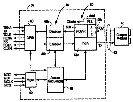
Figure 3 is a block diagram providing a more detailed view of the
components of the modem 32_ Specifically, the modem 32 comprises an
cncoder/decoder (ENDEC) 46 which is responsible for encoding a bit sequence as
a symbol for transmission~over a carrier medium such as the POTS wiring 14.
Similarly, the EIVDEC 46 is responsible for decoding a symbol received from
the
wiring 14 to generate a bit sequence. The encoding and decoding operations
performed by the ENDEC 46 will be described in further detail below. The
ENDEC 46 furthermore supplies both transmit and receive clocks to the
communications controller 34, and overall operation of the ENDEC 46 is under
6
1~'i07i99 15:10 F.~.1 7oJ a0S -X785 CA 02303324 2000-03-08
- _~-- - - .- -.. ~ !~I O1~
DEC 07
~~ '~ ~ / 11~
the control of an access sequencer 48. The access sequencer 48 selects a
general
mode of operation for the ENDEC 46 and for the modem 32 as a whole.
The modem 32 further includes receiver/transmitter circuitry 50, which is
responsible for the reception and transmission of symbols encoding bit
sequences.
In one embodiment of the invention, such symbols are delimited by electrical
pulses, in which case a transmitter 50a receives symbol and polarity
information,
synchronized to a master clock, from the ENDEC 46. In one embodiment, the
symbol information received from the ENDEC 46 represents the variable-duration
(or encoding) portion of an electrical composite symbol to be propagated from
the
transmitter 50a. The transmitter 50a appends a fixed-duration (or buffer)
portion
to the variable-duration portion to generate a composite symbol. The
transmitter
50a then generates symbol delimiters, which determine the time duration and
polarity of the composite symbol, in the form of pulse doublets_ Each pulse
~doublct comprises first and second portions of approximately equal duration
and
opposite~polarity, and has a fixed pulse width. The polarity of each pulse
doublet
is determined by information received from the ENDEC 46. As each pulse
doublet comprises two equal portions of equal duration and opposite polarity,
no
Direct Current (DC) component is generated on the wiring 14 when the pulse
doublet is transmitted thereon. Compliance with FCC Part 68 requires that the
voltage levels of each pulse doublet be substantially less than would be
generated
when driving the coupler module 40 at Transistor-Transistor Logic (TTL)
levels.
A reduction in the voltage levels of each pulse may be accomplished by
incorporating a series of resistors, or step-down windings, in a coupling
transformer within the circuitry 50. In one embodiment, each pulse doublet
comprises a single cycle of a 2 MHa sine wave.
The circuitry 50 also includes a receiver 50b, which comprises gain
elements, comparator and digital control circuitry. The receiver 50b produces
an
output pulse, shown at 51 in Figure 7, coincident with the first peak (i.e.
the
inflection point) of a complex waveform received by the wall jack 20 off the
wiring 14. Figure 7 provides an illustrative example of a wavcform 52 that may
be received at the receiver 50b off the wiring 14. The waveform 52 may be
highly
attenuated and distorted as a result of being propagated through a residential
7
1:/07/99 15:10 FaJ 703 30g .~7g5 CA 02303324 2000-03-08
_ -_- . ' -.- -- --. .- -. - _ ~ O 1=~
DE ~0~ ~ 9 11: 07R
. .
POTS wiring 14. As shown at point 54, reflections can result in a peak
amplitude
occurring sometime after arrival of the incident energy. Without line
terminations
and with complex topologies, pulse energy can continue for many microseconds,
decaying gradually.
As mentioned above, the present invention proposes encoding a bit
sequence as a symbol, the symbol having a time duration indicative of the bit
sequence and being determined by first and second delimiters. In one
embodiment of the invention, these delimiters comprise electrical pulses
transmitted from a transmitter SOa. Thus, in order to successfully receive a
symbol at the receiver SOb, the~original pulses generated from a transmitter
SOa
must be as accurately reproduced as possible. To this end, the receiver SOb is
required to detect the first peak of any incident waveform, as the precise
time of
arrival of these incident peaks must be determined to ascertain the time
duration of
a symbol. Accordingly, the receiver SOb is configured to detect the first
incident
peak, such~as the peak 56, of the incident waveform 52, and to ignore
potentially
high amplitude pulses occurring soon after such an incident peak. Further
details
regarding the functioning of the receiver are provide below.
Turning again to Figure 3, the modem 32 also includes system interfaces
in the form of a General Purpose Serial Interface (GPSI) 60 and a management
interface 62. The GPSI 60 allows the modem 32 to control the clocking of data
into and out of the communications controller 34. Table 1 below provides the
details of the GPSI 60 signal lines:
B 1
nr",' /r ;r((f;.w~ p~~~,, v' .:;~: ::' W
r..~: );Jr' ~~,i hr. . J' 'i rrPy
lvr7.,x. 7 .,G ~~:;:'. , 'i 71. ~ W
~~~i..":.,y. ; y' ~yE ;,y:'.~n .iO.y(~~
~., ~;~~r!;r ' ~ j ~ F,.r. 2 r
',J.E<:,~ . ~...a,.h ,~.,,..sn~~~a;(~cr~,
r, r, I;r.a I J , .. :
c; , ~ hy
uJ ' ~
n k
~
.~; ;.c. ~ ; :;.~;~ry
: ~ nr. .; .~,:
rNaiae.,:!~.~,.::;f~!.r'..1 ~ ~escn ZioW:~r~:%~
ts~tion ,.
'!~s.
TENA To Modem Transmit Enable.
Qualifies TX
as
concainin acket
data
TX To Modem Transmit data
to encoder
8
12i07i99 15:11 F..13: 703 JOS 4785 CA 02303324 2000-03-08
_- - --.--.-.-. .--. - --..- -. --. !~ 015
' DEC 0~ '99
~'/~ '~ ~i ~ 1
~~_ '°' ;: :, R 1999
~ . ~ I
TCLK From Modem Transmit Clock.
Runs
continuously
when
T?~NA deasscrted,
stopped while
Access
II7, (detailed
below)
. runs at variable
rate
under control
of
transmit encoder
during
transmission-
RENA From Modem Receive Enable.
Qualifies RX
as
containin acket
data.
RX From Modem Rtceivc data
from
decoder.
RCLK From Modem Receive Clock.
Runs
continuously
when the
wire is idle,
is stopped
during reception
of an
Access ID (detailed
below), runs
at variable
rate under control
of the
decoder during
packet
reCe ClOn.
CLSN From Modem Collision Sense.
Indicates either
a
transmit or
receive mode
collision.
The management interface 62 is a simple 4-wire serial interface for setting
and reading management configuration information. A microprocessor within the
communications controller 34 uses this interface to establish the sped of
operation, and to set the access sequencer's 48 mode of operation. In one
9
~L~~
12;07/99 15:11 F.~.1 70J 908 4785 CA 02303324 2000-03-08
- --, --- -. -.-- --- -- .--.--.. l~J O1B
DEC 07 '99 11~07AM
~98/I446Z
;~ ~ ; : ;~.~ ~n~r~~
';_,; .a ; ~ _.., .
embodiment the communications controller 34 is an ethernet controller, and the
management parameters for the modem 32 are stored in a serial EEPROM, and
loaded automatically every time the controller 34 is reset or initialized.
Table 2
below details the relevant signal pins and management configuration data:
TABLE 2
''. ~/71,''~.v;:1''v'n'I. ~' ..:y~JIy,. yW, ~ ~:.I.,.~~~
':.h~ '~, .''~'.,~, 'yI yS I~.:P,~/!.
. "~ ~ 1
~Si~~i 'n ...:.;:.r:
~~i va r ...,L:..
e r '
'% C'o' i
' ~ ~
'' ~' 9"
' ~
:' i; ;
tal ... ~~,
d SDi ,
n e .
.. ;- -;:
. n ,;..." ,D,escm~
n' tioa.., ..~,
~ ..., ,-,r.
MDO From Modem Serial data
stream
readout of modem
configuration
ate.IIleteTS.
MDI To.Modem Serial data
stream
settings of
modem
.' configuration
ammeters.
MCLK To Modem Serial data
clock. Data
is shifted in/out
on the
rising edge
of this
si aI_
MCS To Modem Chip select.
Qualifies
. and frames activity
on
the serial data
channel.
First data bit
is
rccelved/transtnitted
following assertion
of
_, this signal.
Configuration
data is
loaded into
internal
registers upon
transition
to deasserted
state.
12; 07199 15:11 F.-11 70J J08 :~7g5 CA 02303324 2000-03-08
_-- . ~ ------- _----- 01017
DEC 07 '9~ 11:0GM
~ ~ ~ ~''t,~~.
. .
;... : , . ::::~ .. .
The receiver SOb further includes an Analog Front End (AFE) SOc and a
Phase-lock loop (PLL) circuit SOd. The AFE SOc shapes transmit pulses, and
finds and indicates to the receiver SOb the time (temporal) location of the
incident
peak of a received waveform (pulse).
Figure 4 illustrates the modem 32 included within an adapter 64, which
allows a computer 22 including a lOBaseT Ethernet communications controller to
communicate over a LAN implemented using POTS wiring 14. The adapter 64
includes a filter/coupler module 66, a lOBaseT Media Access Unit (MAU), an
ENDEC 68, an Ethernet MAC Controller 70, a buffer manager 72, and a Static
Random Access Memory (SRAM) 74. The adapter 64 acts as a non-filtering
bridge, and receives packets from either interface, buffers such packets
temporarily, and transmits them to the opposite interface as soon as possible.
Specifically, the buffer manager 72 uses the SRAM 74 to emulate two large FIFO
memories buffering packets being transferred between lOBaseT and the POTS
wiring 14. In one embodiment, the adapter 64 does not have a MAC LAN
address. The adapter 64 further includes a RJ-4-5 connector 76 for lOBaseT
access, and two R3-11 connectors 78. A speed selector 80 allows a user to
configure the transmission speed of the adapter 64. The adapter 84 also
includes
an array of diagnostic Light Emitting Diodes (LEDs) 82.
Encoding
As a result of the arbitrary topology and the unterminated nature of the
POTS wiring, the present invention proposes encoding predetermined bit
sequences as respective symbols for transmission. In one embodiment, each
symbol is distinguished by having a specific time duraxion, this time duration
being determined by the time interval between the receipt of first and second
delimiters, in the form of electrical pulses. The present invention proposes
encoding data in the precise time arrivals of short duration pulses which are
widely separated in time. As described about, a transmitted pulse is
attenuated
and scattered as it bounces around the wiring 14. After enough time has
elapsed,
the pulse wih die out and another can be sent without fear of interference
from the
11
12i07i99. 15:11 F.-11 70J J08 1785 CA 02303324 2000-03-08 - f~j018
07'99 'alb! VAG~._
_ r,._;, .,, ~ - ~. ,~ ~R. ~~c.?~l.
~~ ~~ z~~
previous pulse_ Specifically, once the reflections resulting from a particular
pulse
drop below a receiver's sensitivity threshold, another pulse can be sent
without
risking inter-symbol interference. Reference is now made to Figure 7 which
shows the waveform 52 received at a receiver SOb in response to the
transmission
of a sinusoidal pulse from a transmitter SOa. As illustrated, in one
embodiment of
the present invention receiver s sensitivity threshold may decay exponentially
after
detection of a first peak 56.
For the purposes of this specification, it is convenient to specify a time
unit in which the time between the transmission of pulses can be expressed. To
this end, a time unit arbitrarily termed a TIC is defined as comprising 0.1167
microseconds.
Referring now specifically to Figure 5, a series of sequential symbols 90a-
90c are shown to be separated and distinguished by a series of pulses 92a-92c
transmitted from a receiver SOb over the wising 14. Each symbol 90 has a
predetermined duration indicative of a respective bit sequence. A minimum time
must separate each of the pulses 92 from a preceding pulse, so as to allow
reflections resulting from the pulse 92 to decay below a receiver's threshold.
This
minimum time is included within each symbol 90, as a fixed-duration (or
buffer)
symbol portion, and may be conveniently referred to as an Inter-Symbol
Blanking
Interval (ISBI) 94. The duration of the ISBI 94 is determined by a number of
factors, such as the complexity of the POTS wiring topology, the impedance of
terminators (c_g., telephones) on the ends of each wiring branch, and random
noise
on the line which may add to the amplitude of decaying reflections. In one
exemplary embodiment, the ISBI 94 has a duration of between 1 and 5
microseconds, and specifically of 2.1 microseconds (i.e. 20 TICS within a
modem
32 operating at 60 MHz.) It will be appreciated that the ISBI 94 effects the
transmission data rate, and it is desirable to have the ISBI 94 as short as
possible.
Each symbol 90 is furthermore shown to comprise a variable duration
symbol portion 96 indicative of a predetermined bit sequence. The symbol
portion 96 may be expressed as an integer multiple of the TIC time interval,
and
the duration of a symbol may thus be expressed as ISBI+D*TIC, where D is an
integer.
12
12:'07/99 15:12 F..~ 703 JOg 47g5 CA 02303324 2000-03-08
.- , ' -.- - . - --. 01019
~ ~ ~ X11= 07RM
An exemplary method of encoding a bit stream as a sequence of symbols
90 will now be described with reference to Figure 6. Specifically Figure 6
shows
a coding tree 100 illustrating a method a coding a bit strcam_ The encoding is
performed by the ENDEC 46, which includes a shift register receiving bit
stream
102 from the communications controller 34 via the GPSI 60. For the purposes of
explanation, the encoding of a specific bit sequencx, comprising bits A-G of
bit
stream 102, will be explained- The encoding method begins at step 104 with an
examination of the next bit to be encoded (i.e. bit A). At step 106 a
determination
is made as to whether bit A is a one (1). If so, the next bit (i.e. bit B)
determines
the polarity of a pulse which will comprise a dclirniter of a symbol
representing
bits A-E. The next three bits (i.e. bits C-E) select one of a first set of
eight
symbols (Symbols 1-8). Each of the Synbols 1-8 includes the fixed ISBI 94, as
well as the variable duration symbol portion 96.
Alternatively, if it is determined at step 106 that bit A is a zero, the
method
proceeds to step 108, where a determination is made as to whether bit B is a
one
or a zero. if bit B is a one, then bit C determines the pulse polarity and the
next
three bits (i.e, bits D, E and F) select one of eight symbols in a second
group
(Symbols 9-16).
If both bit A and bit B are zeros, then the method proceeds to step 110,
where a determination is made as to whether bit C is a one or a zero. Tf bit C
is a
one, then bit D determines the pulse polarity and the next three bits (i.e.
bits E, F
and G) select which of a third group of eight symbols (Symbols 17-24) is
selected
to encode the bit pattern. If bits A, B and C arc all zeros, then bit D
selects the
polarity and a Symbol 0 is selected to represent the bit pattern.
Accordingly, it will be appreciated that Symbol 0 encodes a 4-bit sequence
GOOD, Symbols 1-8 encode a 5-bit sequence 1BCDE, Symbols 9-16 encode a 6-bit
sequence O1CDEF and Symbols 17-24 encode a 7-bit sequence OO1DEFG.
The encoding method thus encodes bit sequences in groups of varying
sizes, specifically in groups either 4, 5, 6, or 7 bits. The symbols are
assigned to
the encoded bit sequences in a manner which causes more data bits to be
encoded
in symbols having a greater duration. For example, symbols 17-24 will include
variable-duration portions 96 which are longer in duration than the variable-
13
Apm Sue'
12:07/99 15:12 F..~ 703 303 4755 CA 02303324 2000-03-08
--.,.--- .- --.-. -.-- -. - ~ 0 2 0
DEC 07 '99 11:0?R
' ~~~~f'~~~99
duration symbol portions of Symbols 1-8_ This allows optimal average and
minimum bit rates to be achieved. The encoding of a bit utilizing the polarity
of a
pulse which acts as a delimiter for the symbol also contnbutes towards
optimization of the encoding methodology.
Figures 8a, 8b and 9a illustrate an exemplary embodiment of the modem
32 implemented using Field Programmable Gate Arrays (FPGAs). The encoder
46A is shown in Figure 9a to comprise an encode state machine 116 and a token-
to-symbol conversion circuit 118. The encode state machine receives a TIC
clock
(TCLK) signal 120, and a Master State (MS [7:0]) signal 122 which indicates
the
master state of the modem 32 and is generated by the access sequencer 48. The
encode state machine 116 also receives data to be encoded via input (GN_DATA)
124 from the communications controller 34 via the GPSI 60. The outputs of the
encode state machine 116 include the following signals:
1. ~ Pulse 126: Assertion of this signal instructs the transmitter to send
a pulse and to accept a next symbol for transmission;
2. NG_SE signal 128: Assertion of this signal informs the GPSI 60 to
shift out another bit;
3. NT POL 132: This signal represents the data bit which follows the bits
used to select the group of symbol from which the transmitted symbol is
selected,
and sets the polarity of the next symbol delimiter (or pulse);
4. TSET [ 1:0] signal 130: This signal encodes whether the next bits are
000,01 or 001 (i.e. selects the set of eight symbols from which the symbol is
selected); and
5. TSEL [2:0] signal 134: This signal comprises the three select bits
following the polarity bit indicated by the NT_ POL signal 132 and is used to
select a symbol from within a group of eight symbols.
The token-to-symbol conversion circuit 118 receives the TSET [1:0] signal
130 and the TSEL [2:0] signal 134 from the state machine 116, and generates
the
symbol to be transmitted, represented by the NT_SYM [4:0] signal 136. The
symbol (i.e. the NT_SYM [4:0] signal 136) is propagated to the transmitter
SOa., as
shown in Figures 8a and 8b, which adds to this symbol the ISBI portion 94 to
thereby generate the composite symbol The transmitter SOa waits for a number
of
14
12107/99 1:12 F..~.1 70J 308 -1785 CA 02303324 2000-03-08
__----- - -.-- - - - _.-. - .- _ --. '_- DEC 07 ~ 021
I 199 11:0~AM
~I"Tr lt~
': , ,~;v i:
~~1~ w ~ ~ "-~ 199
TICs represented by this composite signal between the transmission of
delimiter
pulses.
Operation of the embodiment of the encoder 46a shown in Figures 8a, 8b
and 9 will now briefly be described. Firstly, the NT_pulse signal 126 is
asserted,
causing a pulse to be transmitted from the transmitter 50a. The transmitter
furtber
includes an interpulse timer (not shown) which begins a timed record from
issuance of this pulse. Next, the shift register within the encoder state
machine
116 is reset and the NG_SE signal 128 is asserted to receive a bit from the
GPSI
60_ The contents of the shift register are then shifted to the left and
examined
until one of four patterns is recognized (i.e. 000,1,01,001). If one of these
patterns
is found, shifting stops and decoding logic within the cncodez 46a encodes the
bit
patent as a number "0..3". The TSEL2..TSELO and NT POL signals are then
outputted to indicate the symbol select and the polarity. External
combinational
logic in the encoder 46a (i.e. the conversion circuit 118) and the transmitter
SOa
convert this information into a number of TICS between pulses need to encode
the bit sequence. Specifically, the transmitter SOa receives pulse and
polarity
information synchronized to the TIC clock signal 122 and then generates a
pulse
doublet, which comprises a sinusoidal pulse of a fixed width and of a polarity
determined by the NT_POL signal 132. The transmitter 50a transmits this pulse
on the TXP and TXN outputs. The time at which to generate this delimiting
pulse
is determined in accordance with the symbol information sent to the
transmitter
50a by the encoder 46a and in accordance with the transmitter inter-pulse
timer.
Decoding
Referring again to Figures 8a, 8b and to Figure 9B, in response to the
transmission of a sinusoidal pulse doublet from a transmitter SOa coupled the
POTS wiring 14, a response waveform 150, such as that shown in Figure 7, is
received at a receiver SOb. In order to determine the time duration between
transmitted pulses, the receiver 54b is required to determine the precise time
of
arrival of incident peaks, such as the incident peak 56 shown in Figure 7. In
one
exemplary embodiment, the main receiver signal path consists of an amplifier
followed by a differentiator (not shown). The amplifier may be necessary to
AtiEAdO~
ic- a I i b.y 1J: 1J l i.1 ! UJ JUO =~ ('Sj CA 02303324 2000-03.-08--_-, f~
022
-- - ~ '-"-- - . DEC 07 ' 99 ~ 1 l ' 07A
~''~p~ ~ ~' "-~?~ 1999
compensate for the low transmit levels required for compliance with FCC Part
68,
and gain is accordingly fixed at about l5dB. The output of the amplifier is
fed to
a differentiator, whose output changes polarity whenever the input waveforrri
s
slope changes sign. The output of the differentiator is gated by both time and
amplitude processing circuits within the receiver 50b. Following the detection
of
a peak, a timer (which times the ISBI interval 94) is started. During this
time the
receiver 50b is disarmed. Peaks within the received waveform 150 are ignored
during the ISBI interval, even if the amplitudes are greater than that of the
originally detected peak.
The differentiator tray be sensitive to noise and thus susceptible to
producing spurious outputs during the ISBI period. In one exemplary
embodiment, to further qualify the output of the diffcrentiator, two
comparators
and a "peak following" threshold generating circuit (not shown) detect the
polarity
of an incoming pulse. The comparators take as inputs the amplified waveform
and a threshold voltage. The comparators receive opposite phases of the
amplified
input waveform, so that one comparatoi s output is active when the waveform
exceeds the threshold in a positive direction, and the other comparator's
output is
active when the waveform exceeds the threshold in a negative direction. The
threshold voltage, generated by the threshold generating circuit, tracla the
amplitude of the incident peak 56. ~ Once the incident peak 56 passes, the
threshold
voltage may be allowed to decay exponentially, as shown in Figure 7, in a
manner
that roughly models the expected lowered amplitude response of received
reflection pulses. A bias ensures that the threshold voltage can only sink to
a
minimum value representing the maximum sensitivity of the receiver 50b. A ,
synchronized digital state machine controls operation of the receiver 50b. The
receiver 50b is again armed when the amplified waveform voltage is blow the
threshold, and the ISBI timer has expired. As a new waveform 152 arrives, the
amplified line voltage rises above, or falls below, the threshold voltage,
causing
one of the two comparators to again become active. This then sets a latch
which
remembers the polarity of the incident wave form, and disables the output of
the
other comparator until the receiver 50b is re-armed. The setting of this latch
causes the threshold voltage to be driven to the peak voltage of the incident
wave.
16
12%o7~s9 13:13 Fas 703 303 :1785 CA 02303324 2000-03-O8
--- -.-- --- -.- ~I 0 ~~ 3
-"---'-'-- =DEC 07 ' 99 11: 07RM.,
r~P ~~
~~ 9
The latch also arms an edge detector circuit (not shown) which is looking
for a transition from the peak detector, indicating the arrival of a first
incident
peak 56. The output of the edged detector is a one-cycle wide pulse
synchronized
to the system clock isolator. Detecting the peak starts the ISBI timer which,
in
turn, holds the comparator latch circuit reset and makes the receiver SOb
blind to
any more input pulses until the ISBI timer expires.
While the receiver 50b is waiting of the next pulse, the~threshold
_ generating circuit output is in a high impedance state, allowing a capacitor
to hold
the threshold voltage. A bleed resistor causes this voltage to drain off,
effectively
increasing the sensitivity of the receiver 50b witb the passing of time from
the last
pulse.
The decoder 46b performs the reverse of the operation performed by the
encoder 46a. Specifically, the decoder 46b receives the encoding symbol
portion
96 from the receiver SOb and reconstitutes a token (i.e. a set/select pair)
from
which the original bit sequence can be generated. Specifically, the decoder
includes a symbol-to-token conversion circuit 200 and a decode state machine
202
as shown in Figure 9B. The conversion circuit 200 receives the symbol via
input
RD_SYM[4:0] 204 from the receiver SOb, this symbol being derived from the
measured inter-pulse time. Specifically, the receiver 50b identifies a
composite
symbol based on the time duration between succession delimiter pulses, and
subtracts the known fixed-duration (or buffer portion) (ISBI) 94 from the
composite symbol to reveal the encoding portion 96, which is represented by
the
signal on RD SYM[4:0] input. The symbol is converted by the circuit 200 to the
following token outputs:
1. RSET[1:0]: This output indicates the set of eight symbols to which
the relevant symbol belongs; and
2. RSFS.[2.0]: This output indicates which of the symbols in the
selected set comprises the appropriate symbol.
The token values are then fed to the decoder state machine 202 which,
based on the supplied token consisting of a sec, select and polarity,
determines the
length and pattern of the decoded bit sequence. The inputs to the decoder
state
machine 202 include the following:
17
QED Sh6F,
1'~/07i99 15:1J F.~1 703 a08 4785 CA 02303324 2000-03-08
_-- lQ 0 2:~
DEC 07 ~99 ,11
~CTII(~98~1 j~_~
~'"~S ~ ~~~ P ~ 1999
1. RD PULSE 206: This signal indicates to the decode state machine
202 that a symbol pulse has been detected; and
2. 12D_POL 208: This signal indicates the polarity bit of the pulse.
Outputs of the decode state machine 202 include the following:
1. DG_DATA 210: The decoded bit sequence is sent to the
communications controller, via the GPSI 60, on this output; and
2. DG_SE 212: This output tells the GPSI 60 to shift in another bit.
While the above exemplary embodiment has been reali2ed utilizing
FPGAs, it will readily be appreciated that the circuitry and functional units
described above may readily be incorporated within an Application Specific
Integrated Circuit (ASIC).
Thus, a method and apparatus for encoding and decoding a bit sequence
for transmission over a POTS wiring have been described. Although the present
invention has been described with reference to specific exemplary embodiments,
it
will be evident that various modifications and changes may be made to these
embodiments without departing from the broader scope and spirit of the
invention.
Accordingly, the specification and drawings are to be regarded in an
illustrative
rather tban a restrictive sense.
18