Note: Descriptions are shown in the official language in which they were submitted.
CA 02304028 2000-04-OS
METHOD FOR FORMING THIN FILM, SPHEROID COATED WITH THIN
FILM, LIGHT BULB USING THE SPHEROID AND EQUIPMENT FOR
FILM FORMATION
FIELD OF THE INVENTION
The present invention relates to a method for forming infrared
reflection films used for light sources such as incandescent lamps or
tungsten-halogen lamps. The present invention relates also highly efficient
light sources as light bulbs provided with the infrared reflection films.
BACKGROUND OF THE INVENTION
'Journal of Illuminating Engineering Society', July 1980 (p.197-203)
or some other documents have suggested methods for providing low power
incandescent lamps and tungsten-halogen lamps. For this purpose, light
bulbs are coated with infrared reflection films to substantially pass only
visible light that is selected from light beams emitted from filament portions
of the light bulbs.
In this method, a maximum proportion of the infrared reflection light,
which appears to compose 70-80% of the radiation energy, can be reflected
inside of the light bulb. The reflected light is focused on the filament coil
portion to heat the same portion. Since the filament coil portion is re-
heated in this manner, the consumed power is reduced by 20-30% in
comparison with a conventional light bulb when the illuminance (total value
of luminous flux) from the filament portions is equivalent.
Such an infrared reflection film includes an interference multilayer
film having a laminate of transparent dielectric thin films with high
refractive index and low refractive index. The interference multilayer film
decreases infrared rays escaping as heat rays from the light bulb, and it
selectively passes visible light only, so that the infrared rays can be
reflected
effectively.
To form infrared reflection films with the best uniformity on three-
dimensional objects (in many cases, spheroids) such as light bulbs, various
methods such as CVD, evaporation or sputtering are used.
In the above-mentioned interference multilayer films, the films are
required to be coated with an accurate thickness while they have desired
refractive indices. Evaporation and sputtering are useful in forming thin
films with a controlled thickness on conventional flat substrates. However,
1
CA 02304028 2000-04-OS
the methods are not suitable for forming thin films with a uniform thickness
on three-dimensional objects including spheroids such as light bulbs.
In a case of a three-dimensional object, generally, the distance from
the object to either an evaporation source or a sputtering target can vary.
Moreover, the other side (the side away from the evaporation source or the
target) of the object should be also coated with a film. As a result, the film
has a considerably uneven thickness, and the multilayer film cannot show its
functions, and the efficiency of the infrared ray reflection will deteriorate.
Furthermore, visible light of a wavelength to be transmitted is
reflected excessively due to the film with uneven thickness. As a result,
problems such as coloration and color unevenness will occur in the electric
light source.
CVD is used for forming thin films by using starting molecules which
are supplied as a gas flow from substantially all directions rather than a
specific direction. This method can provide comparatively uniform film
thickness without any special difficulties. However, CVD also presents
several problems, for example, the absolute value of the film thickness
cannot be controlled sufficiently. In addition, the object will be heated
inevitably, and the material gasses or the conditions should be changed for
the respective films composing a laminate.
SUMMARY OF THE INVENTION
To solve the problems, the present invention provides a method for
forming thin films with a uniform thickness on substrates including
spheroids even by film-forming methods such as evaporation or sputtering.
In evaporation or sputtering, incident particles as film materials will be
supplied from a specific direction. The present invention also provides a
spheroid coated with a film of the method, a light bulb including the spheroid
and equipment for film formation.
In order to achieve the purpose, the method for forming thin films
according to the present invention includes forming a thin film on a
substrate including a spheroid with an incident particle beam coming from a
particle source located in a specific direction when viewed from the
substrate.
In this method, a spin motion and a swing motion are performed together.
The spin motion is a rotation of the substrate at a constant angular velocity
about the spheroidal axis. Here, 'spheroidal axis' refers to the central axis
of the rotation of a spheroid. The swing motion is a rotational oscillation of
2
CA 02304028 2000-04-OS
the same substrate for rotationally oscillating the axis at a constant cycle
in
one surface, where the center of the rotational oscillation is in the vicinity
of
the midpoint between two focal points on the axis of the spheroid.
In the method using a spin motion and a swing motion together, a
thin film that has a uniform thickness in the peripheral direction of the
substrate and in the rotational direction of the spin motion can be formed
even if the substrate comprises a spheroid.
It is preferable in the method that the swing motion is performed to
get the part of the substrate below the midpoint of the axis positioned away
from the particle source when the upper part of the same axis approaches the
particle source, so that the uniformity of the thin film in the rotational
axis
direction is further assured.
It is also preferable that the particle source is a flat plate and the
swing motion is performed to rotationally oscillate the axis at a constant
cycle in a surface perpendicular to the flat plate surface, so that the
uniformity of the thin film in the rotational axis direction is further
assured.
It is preferable that the rotational angular velocity of the rotational
oscillation of the swing motion is varied continuously, so that the rotational
velocity of the swing motion can be set to be suitable for the distance
distribution between the substrate surface and the particle source surface.
It is preferable that the rotational oscillation is varied intermittently
by setting plural stationary positions within the rotational oscillation range
and also stationary times at the respective positions, so that the swing
motion can be performed easily.
It is preferable that the thin film is formed by either sputtering or
evaporation.
It is preferable that the thin film is at least one selected from the
group consisting of an infrared reflection film and a frost film.
It is also preferable that the substrate including a spheroid is a light
bulb.
It is preferable that the center of the rotational oscillation of the
swing motion is in the vicinity of the longitudinal center of the filament
portion of the light bulb.
A spheroid of the present invention is coated with a thin film, and the
thin film is formed with an incident particle beam coming from a particle
source located in a specific direction when viewed from the spheroid as an
object. The spheroid is subjected to a spin motion together with a swing
3
CA 02304028 2000-04-OS
motion in order to form a thin film thereon. The spin motion is a rotation of
the spheroid at a constant angular velocity about the spheroidal axis. The
swing motion is a rotational oscillation of the same spheroid for rotationally
oscillating the axis at a constant cycle in one surface, where the center of
the
rotational oscillation is in the vicinity of the midpoint between two focal
points on the axis of the spheroid. The thin film has a uniform thickness at
least in the rotational direction of the spin motion and also in the
rotational
oscillation direction of the swing motion.
The spheroid coated with the thin film is useful for light bulbs due to
the uniformity in the film thickness.
It is preferable in the spheroid that the swing motion is performed to
get the part of the spheroid below the midpoint of the axis positioned away
from the particle source when the upper part of the same axis approaches the
particle source, so that the uniformity of the thin film in the rotational
axis
direction is further assured.
It is also preferable that the particle source is a flat plate and the
swing motion is performed to rotationally oscillate the axis at a constant
cycle in a surface perpendicular to the flat plate surface, so that the
uniformity of the thin film in the rotational axis direction is further
assured.
It is preferable that the thin film is formed by sputtering or by
evaporation.
It is also preferable that the thin film is at least one selected from the
group consisting of an infrared reflection film and a frost film.
It is preferable that the spheroid is a light bulb.
It is preferable that the center of the rotational oscillation of the
swing motion is in the vicinity of the longitudinal center of the filament
portion of the light bulb.
A light bulb of the present invention includes a spheroid coated with
a thin film. The film on the light bulb is substantially uniform in thickness,
since it is formed with an incident particle beam coming from a specific
direction while the spheroid (light bulb) is subjected to a swing motion
together with a spin motion. In order to meet the requirement for the
uniformity, the film thickness on the spheroidal substrate in a range of
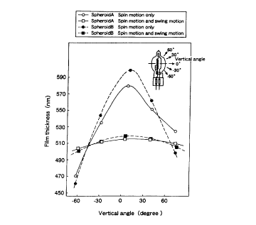
f60°
from the vertical angle (see the upper right-hand in the graph of FIG. 1) is
at
least 88% of the maximum film thickness, i.e., t6% to the medium value.
When the thin film is a laminate comprising transparent dielectric thin films
differing in their refractive indices, the light bulb can be prevented from
4
CA 02304028 2000-04-OS
being colored or having color unevenness, and the energy will be saved
considerably.
Film-formation equipment of the present invention is used to form
thin films having a uniform thickness on substrates comprising spheroids
with an incident particle beam coming from a particle source located in a
specific direction when viewed from the substrates. The equipment is
provided with a rotational mechanism to perform a spin motion together
with a swing motion. The spin motion is a rotation of the spheroid at a
constant angular velocity about the spheroidal axis. The swing motion is a
rotational oscillation of the same spheroid for rotationally oscillating the
axis
at a constant cycle in one surface, where the center of the rotational
oscillation is in the vicinity of the midpoint between two focal points on the
axis of the spheroid.
It is preferable that the equipment uses RF (radio frequency)
sputtering or DC (direct current) sputtering in the film formation process.
BRIEF DESCRIPTION OF THE DRAWINGS
FIG. 1 is a graph to show a relationship between the vertical angle on
a light bulb and the thickness of a film, where the film is formed by the
method in a first embodiment of the present invention.
FIG. 2 is a graph to show a relationship between the rotational angle
along the periphery of a bulb and the film thickness, where the thin film is
formed by the method in the first embodiment of the present invention.
FIGS. 3A and 3B are schematic views to show light bulbs to be coated
with thin films by the methods of the present invention.
FIG. 4 is a graph to exemplify a swing motion in film formation
according to the first embodiment.
FIG. 5 is a graph to show a relationship between the vertical angle on
a light bulb and the thickness of a film, where the film is formed by the
method in a second embodiment of the present invention.
FIG. 6 is a graph to exemplify a swing motion in film formation
according to the second embodiment.
DETAILED DESCRIPTION OF THE INVENTION
Embodiments of the present invention are explained specifically
below by referring to FIGs. 1-6. FIGs. 3A and 3B exemplify the
configurations of light bulbs used in the embodiments. Both a light bulb 1
5
CA 02304028 2000-04-OS
in FIG. 3A and a light bulb 4 in FIG. 3B include spheroids. Filaments in the
light bulbs focus infrared rays. Since the length of the filaments is
restricted in view of energy-saving, a typical light bulb includes a spheroid
having a proper ratio of the long axis to the short axis. Hereinafter, the
figure of the light bulb 1 is referred to as "spheroid A" while that of the
light
bulb 4, which is a substantial sphere, is referred to as "spheroid B".
The light bulbs have filaments 3, 6 and electrode terminals 2, 5
respectively. "P" in FIG. 3A indicates a midpoint between two focal points
(Q and R) on the rotational axis of the spheroid. FIG. 3B also has a similar
midpoint though it is not shown. The midpoint P is typically located on a
filament coil in the longitudinal direction.
First Embod,_'m n .
In this embodiment, an SiO~ thin film was formed on a light bulb
with RF sputtering. The target was a flat plate 200mm in width and
900mm in length.
A spin motion and a swing motion were performed together to
prevent the film on the light bulb from having uneven thickness. The spin
motion is a rotation of the light bulb at a constant angular velocity about
the
spheroidal axis. The swing motion is a rotational oscillation of the same
light bulb for rotationally oscillating the axis at a constant cycle in one
surface, where the center of the rotational oscillation is the midpoint P In
the spin motion, the spheroid rotates about the axis of the filament at a
regular angular velocity of 100rpm.
Though the spin motion can provide a thin film with a thickness
uniform in the rotational direction, a swing motion should be carried out
together with the spin motion in order to provide a film with a thickness
uniform in the rotational axis direction.
The swing motion is a rotational oscillation at a constant cycle, where
the spheroidal axis undulates at X60 degrees from the midpoint P in a
surface parallel to the flat plate target (see, the upper right-hand in the
graph of FIG. 1). The swing motion is not effective if the rotational
amplitude surface is parallel to the target surface. In the First
Embodiment, the rotational axis of the spheroid is set to move in a surface
perpendicular to the target surface. More specifically, the axis oscillates
rotationally so that the part of the spheroid below the midpoint P of the
spheroidal axis is positioned away from the flat plate target when the part
above the midpoint P of the same axis approaches the flat plate target during
6
CA 02304028 2000-04-OS
the swing motion.
The rotational velocity of the swing motion should be set
corresponding to the distance distribution between the substrate surface and
the flat plate target surface, since the distance depends on the spheroidal
shape in the rotational axis direction of the light bulb (an object). When the
spheroid is made to be a substantial sphere (spheroid B), the swing motion
substantially becomes a simple harmonic oscillation.
In the First Embodiment, one cycle of the swing motion is 20 seconds,
and the swing angle of the rotational axis shifts in one cycle as indicated in
FIG. 4 (hereinafter, it is called "a continuous swing mode"). The solid line
in
FIG. 4 indicates a continuous swing mode for a light bulb with a spheroid A,
while the broken line indicates the same for a light bulb with a spheroid B.
FIGS. 1 and 2 shows results of measurement on the film thickness
distribution for the spheroids A and B, where a spin motion was performed
alone or together with a swing motion. The distance between the flat plate
target surface and the rotational axis of spheroids (light bulb filaments) was
set to be 90mm.
FIG. 1 shows the thickness distribution of a film formed on spheroids
of light bulbs in the rotational axis direction. FIG. 1 shows also a
measurement result as a comparative example obtained by forming a film
using only a spin motion but not a swing motion. FIG. 2 shows a thickness
distribution of a film in the direction of the cross-sectional circumferential
direction (spin rotational direction) perpendicular to the rotational axis.
The ordinate in FIG. 1 indicates thickness (nm) of an Si02 film. The
abscissa indicates positions of a light bulb surface corresponding to vertical
angles (elevation angle) of a surface that is perpendicular to the rotational
axis of a spheroid comprising the midpoint P For the vertical angle, the
direction inverse to the light bulb terminals is determined to be the plus
direction, while the light bulb terminal side is determined to be the minus
direction (see upper right-hand in FIG. 1).
The ordinate in FIG. 2 indicates thickness (nm) of an Si02 film. The
abscissa indicates positions on the light bulb periphery on a surface
perpendicular to the rotational axis of a spheroid including the midpoint P
The zero-degree direction is the position where a mount is provided to the
filament on the rotational axis. The angles are displayed by determining
the counterclockwise direction as the plus direction about the rotational axis
relative to the zero-degree when viewed from the top of the light bulb (right-
7
CA 02304028 2000-04-OS
center in FIG. 2).
FIGS. 1 and 2 show that films can be formed on light bulbs with a
substantial uniformity in both the vertical and horizontal directions when a
swing motion is performed together with a spin motion.
The measurement result in FIG. 1 shows that additional use of a
swing motion is remarkably effective when compared with the result
obtained by using only a spin motion. The problem of uneven thickness of
the thin film formed on a bulb cannot be solved by using a spin motion alone,
especially when the thin film is formed with an incident particle beam
coming from a particle source located in a specific direction when viewed
from the object (e.g., RF sputtering).
Second Embodim .n
In the Second Embodiment, an SiOz thin film was formed on a light
bulb surface by using RF sputtering as in the First Embodiment. This
embodiment is distinguishable from the First Embodiment in that the swing
motion is not a continuous motion as shown in FIG. 4 but an intermittent
motion as shown in FIG. 6 (hereinafter, it is called "a step-swing mode").
In a step-swing mode in FIG. 6, an oscillation angular range of a
rotational oscillation in a swing motion of a predetermined cycle is divided
to
be set as plural stationary angles ( 8 n), and stationary times (tn) for the
respective stationary angular positions are also set. More specifically, the
rotational motion of the swing is set as ( B 1, t1)...( 8 n, tn) within the
range
of the amplitude angles. The step-swing mode can be provided in a simple
manner compared to the continuous swing mode described in the First
Embodiment.
In this embodiment, n=5, and the rotational angular range of the
swing amplitude is set to be ~ 45 degrees to the medium value. As shown in
FIG. 6, the cycle of the rotation is set with a step-swing mode, in which ( 8
1,
tl) _ (-45°, 5.3 seconds); ( 8 2, t2) _ (-30°, 3.2 seconds); ( 8
3, t3) _ (0°, 2.0
seconds); ( 8 4, t4) _ (+3p°, 3.2 seconds); and ( 8 5, t5) _
(+45°, 5.3 seconds).
In the swing motion shown in FIG. 6, rotation is performed from 8 1
to 8 5, and the rotation returns from 8 5 to 8 1, so one cycle is about 28
seconds. The angular velocity for moving between the respective stationary
angular positions can be constant or not. In the Second Embodiment, the
velocity for moving between the respective stationary angular positions is
substantially constant, and the time required for the move is short (within
one second per step) when compared to the stationary time (tn) at each
8
CA 02304028 2000-04-OS
stationary angular position.
FIG. 5 shows a comparison between an example using the step-swing
mode in addition to a spin motion, and a comparative example using a spin
motion alone. Both the example and comparative example include Si02
thin films formed on light bulbs by using RF sputtering as in the First
Embodiment. Here, light bulbs having spheroid A were used. The target
was a flat plate 200mm in width and 900mm in length. In the spin motion,
the spheroid rotates about the axis of the filament at a regular angular
velocity of 100rpm.
The ordinate and abscissa correspond to those in FIG. 1. FIG. 5
shows that a step-swing mode can provide a uniform film thickness as in the
case of a continuous swing mode. The effect is further remarkable when
compared with a comparative example of a film formed by using a spin
motion alone.
As mentioned above, the film-forming methods in the embodiments
provide thin films with a uniform thickness. Therefore, the method for
forming films of the present invention is useful in forming interference
infrared reflection multilayer films or frost films on light bulbs. Such
multilayer films comprise laminates of transparent dielectric multilayer
films differing in the refractive indices.
A 90W tungsten-halogen lamp including a light bulb having a
spheroid was prepared by forming an infrared reflection thin film on the
spheroid by using a method in the present invention. This lamp was used
for a comparison with a tungsten-halogen lamp having the identical total
value of luminous flux (1600 lumen) prepared without using the method of
the present invention. The efficiency of the present invention (lm/W) was
improved by about 30%.
Frost films to soften the glare of the light bulb also were formed
uniformly as the outermost layer on the light bulb.
RF sputtering was used for forming thin films in the embodiments.
The film-forming method is not limited thereto as long as the thin films are
formed with an incident particle beam coming from a particle source located
in a specific direction when viewed from the substrates. Equivalent effects
are obtainable in any other general-purpose sputtering such as DC
sputtering, or various kinds of evaporation.
Thin films in the above-identified embodiments can be formed by
using film-formation equipment having a rotational mechanism for
9
CA 02304028 2000-04-OS
performing a spin motion together with a swing motion, and by combining
the film-forming method with conventional evaporation or sputtering.
Consequently, according to the present invention, a thin film with a
uniform thickness can be formed with accurate control on a substrate even
when incident sputtered particles are supplied from only a specific direction
as in a conventional method such as evaporation and sputtering, or even
when the substrate comprises a spheroid such as a light bulb.
As a result, even a laminate film comprising transparent dielectric
films with different refractive indices can be formed uniformly with accurate
control on a curved surface of a light bulb, an efficient and energy-saving
light bulb can be manufactured, and the light bulb is protected from light
coloration or color unevenness.
The invention may be embodied in other specific forms without
departing from the spirit or essential characteristics thereof. The
embodiments disclosed in this application are to be considered in all respects
as illustrative and not restrictive, the scope of the invention being
indicated
by the appended claims rather than by the foregoing description, all changes
that come within the meaning and range of equivalency of the claims are
intended to be embraced therein.