Note: Descriptions are shown in the official language in which they were submitted.
CA 02304304 2000-03-21
WO 99/I6093 PCT/US98/19279
1
DESCRIPTION
CORE AND COIL STRUCTURE AND METHOD OF MAKING THE SAME
BACKGROUND OF THE INVENTION
1. FIELD OF THE INVENTION
1 o This invention relates generally to inductive devices, and in particular
to a
laminated multi-layered inductive device and method of making the same.
2. DESCRIPTION OF THE RELATED ART
Early microcircuit and designers avoided inductive surface mount components
such as transformers and inductors because of the relatively large physical
size of such
I5 devices. Eventually, micro size inductive components were developed,
however, these
components exhibited extremely low values of inductance (e.g. from nano Henrys
up to
one micro henry}. As a result, they could only be used at high frequencies,
such as for
microwave frequency circuits.
One conventional solution, as illustrated in U.S. Patent 3,765,082 to Zytez,
2 0 attempted to overcome these problems by using a monolithic inductor chip.
However, the
coil design in such conventional solutions is inefficient and is incapable of
obtaining as
high inductance levels as the present invention, because it only uses ferrite
wafers to form
the laminate structure. As a result, high permeable ferrite was generally not
used, as it
tended to short out the conducting lines (e.g. windings) of the device.
SUMMARY
Accordingly, there has been a long felt need in the art for a small sized
inductor,
transformer or other inductive device having high-permeability core, which may
be used in
a broad range of frequency applications.
3 0 In certain embodiments of the invention, the invention facilitates the
construction
of devices having relatively large permeability values and small physical
size, and which
CA 02304304 2000-03-21
WO 99/16093 PCTIUS98/19279
2
are capable of operating at high power levels within low to microwave
frequency ranges.
In certain embodiments, the devices according to the invention are provided
with
dimensions of approximately one-half to one inch per side and SO- 60 mils in
thickness
while maintaining a high level of inductance, such as, for example 20mH.
S In another embodiment, the device can be provided with dimensions of
approximately 100 by 120 mils with a similar thickness, while maintaining a
high level of
inductance, such as, for example, 100mH. In yet another embodiment, the device
can be
provided with dimensions of approximately 40 by 20 mils with a similar
thickness, while
maintaining a high level of inductance, such as, for example, 1 to l OmH.
1 o One aspect of the present invention is the unique winding shape and
dimension of
the inductor coil so as to maximize the magnetic properties of the
ferromagnetic materials
being used.
Another aspect of the present invention is the use of non-conducting, non-
magnetic
wafers such as alumina ceramic wafers which have first holes formed in their
center and
15 second holes formed in their periphery. Conductive ink, such as silver,
copper, gold or
some other suitable conductor, is then printed onto the wafers in a
predetermined pattern.
This may be done by a screen printing process. The second holes (vias) are
also filled
with the conductive ink. The first opening is filled with a ferromagnetic
material, such as,
for example, powdered ferrite. The ferromagnetic material can also be prepared
in the
2 0 form of a printable ink and printed into the first opening.
The predetermined patterns of the conductive ink and the position of the vias
are
selected such that when the ceramic wafers are placed together in a layered
fashion such
that the patterns and vias cooperate to form conductive windings about the
first openings.
As the first openings have been filled with the ferrite material, this results
in a winding
2 5 structure surrounding a ferromagnetic core. Once this laminate structure
has been
completed, top and bottom ceramic wafers are attached to the laminate
structure. Vias can
be used to provide leads to the external portion of the laminate structure,
such as, for
example, to provide surface mount contacts. The entire structure is fired, at
a temperature
sufficient to sinter the ceramic. With the proper choice of ceramic materials,
the sintering
3 0 process shrinks the ceramic and pressurizes the ferromagnetic core.
CA 02304304 2000-03-21
WO 99116093 PCTIUS98/19279
3
To form a toroidal structure, two core areas are provided in the wafers. In
this
embodiment, top and bottom wafers include an area covered in ferromagnetic
material so
as to electrically connect the two ferromagnetic cores at the top and bottom
of laminate
structure.
Because in certain embodiments non-magnetic wafers (such as, for example,
alumina) are used, highly permeable ferromagnetic material may be used to form
the core,
without the concern that the conductive lines will be shorted out by the
ferromagnetic
material. For example, the ferromagnetic material to be used may have 50 ohms-
centimeter resistibility while having up to, for example, 10,000m
permeability. Materials
1 o suitable for such applications can include, for example, iron oxide with a
manganese-zinc
additive.
Furthermore, in one embodiment, the structure is preheated to burn off any
organic
material it contains and to naturally shrink the device thereby compressing
the
ferromagnetic core and achieving better permeability characteristics.
In other embodiments, highly resistive ferromagnetic material is used to form
the
wafers and no separate core is needed. For example, a Zinc-Nickel composition
can be
used to form the wafers. In these embodiments, because there is no separate
core structure
and hence no dielectric forming an insulating barrier between the
ferromagnetic material
and the conductive windings, a lower permeability and higher resistivity
ferromagnetic
material is used. For example, in one embodiment, the wafers have up to 3000 m
permeability and 10'~ ohrns centimeter resistivity.
Another aspect of the present invention is directed to a unique winding design
which achieves enhanced inductance values. In particular, a unique torodial
inductor or a
transformer can be formed according to this aspect of the invention. In this
embodiment, a
2 5 plurality of wafers are formed as follows: For a particular wafer having a
length and width,
two fernte receiving holes are formed which extend in parallel to one another
and are
disposed lengthwise along the wafer. Adjacent to the first of these ferrite
receiving holes,
a first conductive ink pattern is formed thereon which extends substantially
straight and
parallel to the fernte receiving hole. Between the first and second ferrite
holes, a second
3 0 conductive ink pattern is formed. The second conductive ink pattern is
generally U
shaped, wherein its base is approximately parallel to the first conductive ink
pattern, and
CA 02304304 2000-03-21
WO 99/16093 PCT/US98/19279
4
its legs extend away from the first conductive ink pattern. The conductive ink
patterns are
formed such that when two wafers are joined together, such that the patterns
are 180E
apart from one another, they form two separate windings about each core.
A plurality of such wafers are joined together. In an end wafer used in
forming an
S inductor, the winding about the first core is shorted out to the winding of
the second core.
Also, bottom and top plates and bridge plates are attached to the stack. The
bridge plates
include ferromagnetic material disposed thereon such that the first and second
cores are
joined together to form a torpid and a single inductor is formed which is
electrically
equivalent to a single conductor being folded in a U shape with a single
winding turning
about the entire U. For a transformer, windings on wafers in the center of the
stack are
shorted and joining wafers are used to allow the core to continue between the
sets of
windings. Regardless of the device being made, the entire group of wafers is
laminated
and sintered.
For example, in one embodiment, the group of wafers is laminated at a pressure
of
approximately 3000 PSI at a temperature of 80 - 100 degrees Centigrade to form
the
laminate structure. Next, the laminated structure is sintered at high
temperature. This step
pressurizes the core to enhance its permeability. In one embodiment, the
sintering step is
performed at as high a temperature which can be used without melting the
conductive
windings. For example, for a silver or silver alloy conductor, the package is
fired at
2 0 approximately 920 degrees Centigrade. This step causes the dielectric
material to shrink
and further compresses the core, enhancing its permeability.
In one embodiment, the sintering step is performed without added pressure
(e.g., at
one atmosphere).
An additional pre-firing step can be used to burn off organic material in the
wafers.
2 5 In addition, as a result of the firing, the ferromagnetic core and any
bridge plates,
joining plates, and top and bottom plates used will be formed into a single
structure
Consequently, only negligible permeability losses are experienced at the
junction between
the top and bottom plates and the core. This is a great enhancement over the
conventional
devices wherein the top and bottom plates are attached to the core via glue or
other
3 0 mechanical means.
CA 02304304 2000-03-21
WO 99/16093 PCTNS98/19279
In yet another embodiment, post-firing densification can be used after the
sintering
step to provide additional densification of the device structure. In this
embodiment, the
device is heated at high temperatures and pressurized (e.g., 920-degrees
Centigrade for
silver conductors at 3000 PSI). This additional step enhances qualities of the
materials in
5 a single step by using isostatic pressure at high temperature.
Because the wafers used in the described devices are formed into a stack,
careful
placement of the components printed thereon is crucial to provide proper
alignment
throughout the stack.
The terms Atop@ and Abottom@ used in this document refer to relative locations
of the ends of the laminate structure and do not mandate a particular spatial
orientation of
the device with respect to a fixed or variable frame of reference.
BRIEF DESCRIPTION OF THE DRAWINGS
The present invention is now described with reference to the accompanying
drawings. It should be noted that the drawings are not necessarily drawn to
scale.
FIGS. 1 A, 1 B and 1 C are diagrams illustrating three phases of a wafer in
fabrication according to one embodiment of the invention.
FIG. 2 is a diagram illustrating a process for fabricating wafers, such as
wafers
illustrated in FIG. 1, and for assembling the wafers into a device according
to one
embodiment of the invention.
2 5 FIG. 3 is a diagram illustrating an example configuration of stacked
wafers
according to one embodiment of the invention.
FIG. 4 illustrates an alternative configuration, wherein conductors surround
approximately three-sides of the core area according to one embodiment of the
invention.
CA 02304304 2000-03-21
WO 99II6093 PCT/US98/I9279
6
FIG. 5 is a diagram illustrating one example configuration for a wafer
according to
one embodiment of the invention.
FIG. 6 is diagram illustrating a schematic representation of a toroidal effect
which
can be achieved with the example configuration illustrated in FIG. S according
to one
embodiment of the invention.
FIG. 7 is a diagram illustrating a bridge plate including an area of
ferromagnetic
material used to form a bridge according to one embodiment of the invention.
l0
FIGS. 8A and 8B are diagrams illustrating additional alternative
configurations for
wafer according to one embodiment of the invention.
FIG. 8C is a diagram illustrating an alternative configuration for the
embodiments
illustrated in FIGs. 8A and 8B.
FIG. 9 is a diagram illustrating an example configuration or the wafers
illustrated
in Figure 8B according to one embodiment of the invention.
FIG. 10 is a diagram illustrating a tool which can be used for performing the
2 0 operation of stacking wafers and removing the substrate according to one
embodiment of
the invention.
FIG. 11 is a flowchart illustrating a process for using this tool illustrated
in FIG. 10
to create a device according to one embodiment of the invention.
FIGS. 12A and 12B are diagrams illustrating a transformer and an inductor,
respectively, which can be made using wafers 100 configured as illustrated in
FIGS. 8A
and 8B.
CA 02304304 2000-03-21
WO 99/16093 PCTIUS98119279
7
DETAILED DESCRIPTION
The present invention is described with respect to various embodiments;
however,
it should be recognized that these are only provided as specific examples, and
many other
embodiments and designs are within the purview of one of ordinary skill in the
art and
within the scope of the invention.
According to one embodiment of the invention, an inductor, transformer or
other
inductive device is formed with dielectric (for example, ceramic or other non-
conductive
material) wafers having a ferrite or other ferromagnetic core. This embodiment
provides
advantages over conventional ferrite-loaded ceramic devices in that it allows
highly
permeable ferrite to be used without shorting with the conductive windings.
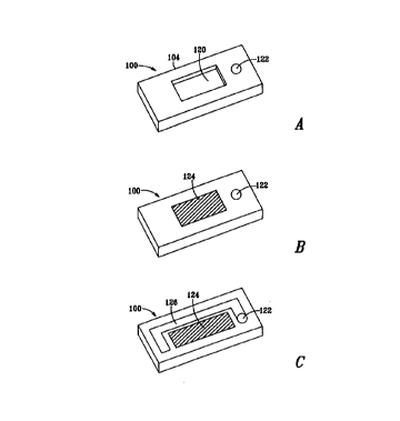
A process of making a device according to one embodiment of the invention is
now described. FIGs. lA, 1B and 1C are diagrams illustrating three phases of a
wafer 100
in fabrication according to one embodiment of the invention. FIG. 2 is a
diagram
illustrating a process for fabricating wafers, such as wafers 100 illustrated
in FIG. 1, and
for assembling wafers 100 into a device.
Referring now to FIGS. 1 A, 1 B, 1 C and 2, in a step 204, a substrate medium,
such
as for example a dielectric material, is prepared as a screen printable ink.
In one
embodiment, alumina is used as the dielectric material. In alternative
embodiments, other
2 0 dielectric materials are used. In this document, the material is referred
to as a Anon-
conductive@ material. As would be apparent to one of ordinary skill in the art
after
reading this description, the resistivity and dielectric characteristics of
the material can be
chosen based on the desired device characteristics.
In a step 208, the dielectric ink is cast into a die section 104. The pattern
2 5 illustrated in FIG. 1 A includes a dielectric die section 104 having a
center void or cavity
120 and a via 122. In the present embodiment where the dielectric material is
prepared as a
printable ink, a die section 104 can be cast by printing the dielectric ink in
a preferred
pattern. In one embodiment, the printing process for printing die section 104
is a screen
printing process, although other printing or casting processes can be used.
3 o The dielectric ink can be printed on a mylar film from which it can later
be
separated. In one embodiment, the thickness of dielectric material is
approximately 1 - 10
CA 02304304 2000-03-21
WO 99116093 PCTIUS98/19279
mils, although other thicknesses can be used. In one embodiment, cavity 120 is
provided
in the dielectric section using a punch, such as, for example, a pneumatically-
controlled
punch.
In a step 212, cavity 120 is filled with a ferromagnetic material 124 such as,
for
example, ferrite. In one embodiment, this is also accomplished using a screen
printing
process to print ferromagnetic material 124, which is prepared as a printable
ink, into
cavity 120. The ferromagnetic material used in one embodiment is a powdered
ferrite
material having a permeability of up to 10,000 m.
In a step 216, a conductive pattern 126 is disposed onto wafer 100 and vial
122. In
one embodiment, this can also be accomplished using a screen printing or other
printing
process. Conventional etching and/or embossing techniques can be used as well
to
increase the cross section of the conductor ink embedded in the ceramic.
Conductive
pattern 126 can be made of copper, silver, gold, palladium silver or other
conductive
material.
The actual layout of conductive patterns 126, cavities 120 and vias 122 are
chosen
based on the type of device desired and its characteristics. Example
alternative
embodiments for different layout arrangements are discussed in detail below,
although
additional alternatives are within the scope of the invention.
In one embodiment, conductive pattern 126 is disposed on the surface of wafer
2 0 100. It is preferable to facilitate close stacking of wafers 100. However,
for performance
reasons it is also desirable to increase the thickness of the conductor to
increase
conductivity. To enable an increase in thickness, in an alternative embodiment
a trench is
created in wafer 100 and the conductive pattern 126 is disposed in this
trench. As such, a
thicker conductive pattern 126 can be used than embodiments where the
conductor is
2 5 disposed on the surface of wafers 100.
In a step 220, a plurality of wafers 100 are combined to create the desired
device.
In this step, wafers 100 are stacked on top of one another such that
ferromagnetic material
within wafers 100 is aligned, thus forming a ferromagnetic core. In one
embodiment, 16
wafers 100 are used, although other quantities can be used as well.
Preferably, the wafers
3 0 are dried at moderate temperatures before stacking. In one embodiment, for
example, the
wafers are dried at SO-degrees Centigrade for approximately five to ten
minutes.
CA 02304304 2000-03-21
WO 99/16093 PCT/US98/19279
9
In one embodiment, the wafers are pressurized during lamination to form the
device structure. For example, the wafers can be pressurized at 3000 PSI and
heated at 80
- 100 degrees Centigrade during lamination.
Preferably, stacked wafers 100 include cover plates, or caps, for the top and
bottom
of the stack and the stack is laminated. As a result, the ferromagnetic core
is completely
encased within a dielectric cavity. Additionally, in embodiments having
multiple cores,
bridge plates (illustrated in FIG. 7) can be used to form a ferromagnetic
bridge between the
cores.
In combining wafers 100, vias 122 are used to electrically connect conductors
126
among wafers 100 to achieve a desired coil or other conductive structure.
Additional
conductors (not illustrated in FIGs lA - 1C) can be disposed on wafers 100 to
interconnect
vial and to enable external connections to conductors 126. The manner in which
conductors 126 are disposed onto wafers 100 and interconnected is discussed in
more
detail below according to several embodiments.
In a step 224, the laminated package is heated at a moderate temperature and
preferably for several hours to remove organic material. The package is next
fired at high
temperature. The high-temperature firing causes shrinkage of the dielectric
material, thus
compressing the core which enhances its permeability characteristics.
For example, in one embodiment, the package is heated at approximately 350
2 0 degrees Centigrade for approximately 20 hours to remove organic material.
The package
is next fired at approximately 920 degrees Centigrade for approximately one
hour to sinter
the package. In one embodiment, the package is not pressurized during these
firing and
heating steps; these steps are performed at ambient pressure. Additionally,
the package
can be further pressurized after firing to enhance structure densification
using, for
2 5 example, isostatic pressure.
To enable the use of high-permeability ferromagnetic material 24, the
invention
takes advantage of a shrinkage factor of the dielectric material which
surrounds the core.
As stated above, the dielectric material shrinks during the sintering process,
compressing
the ferromagnetic core.
3 0 Conventional materials and processes which do not compress the
ferromagnetic
core can suffer from a sublimation of resinous content of the ferromagnetic
material and
CA 02304304 2000-03-21
WO 99/16093 PCT/US98/19279
air gap between the ferromagnetic particles. Such conditions can lead to
decreased device
permeability. In these conventional systems, during the sintering process,
resinous content
of the core is sublimed out of the core, leaving loose particles of
ferromagnetic material
(e.g., ferrite) with a low permeability level. The compression provided
according to the
5 present invention minimizes the sublimation such that the core maintains a
high-degree of
permeability.
For example, alumina as a dielectric material has a shrinkage factor of
approximately 10 - 20 percent. With this material, the core could be compacted
by as
much as 50 percent, depending on the dimensions of the structure, the
sintering
1 o temperatures and other factors.
In addition to the shrinkage factor of the dielectric material, the
compactability of
the core is an important parameter. It is desirable to achieve sufficient
compacting of the
core to achieve high permeability, without shattering the dielectric casing. A
properly
designed package matches the tensile strength of the dielectric material to
the compressive
force of the core to achieve a properly compacted core.
In one embodiment, fernte powder is used to form a ferrite ink. The resin-to-
ferrite
powder ratio of the ferrite used in the process determines the compactability
of the core
and is thus of considerable importance.
Also note that there are tradeoff considerations which must be made when
2 0 considering materials to use and temperature ranges for the process.
Processing the device
at higher temperatures yields a better structure with a better core. However,
higher
temperatures can be destructive to good conductors. Therefore, where higher
device
temperatures are used, generally, a poorer conductor must be used. For
example, silver is
an excellent conductor but can=t be sintered at high temperatures, whereas
palladium is a
2 5 worse conductor which can be sintered at very high temperatures.
Because the compression of the core allows for high permeability levels,
devices
according to the invention can be made smaller than otherwise possible with
conventional
techniques. For example, devices can be made with thicknesses on the order of
50 mils,
which is suitable for most current surface mount applications. One such
application of
3 0 surface mount devices is PCMCIA cards used with laptop computers.
CA 02304304 2000-03-21
WO 99/16093 PCT/LTS98/19279
11
As stated above, a plurality of wafers 100 are stacked and conductors 126 are
connected using vias 122 to form a coil or other desired conductor
configuration. In the
embodiment illustrated in FIG. 1 C, conductor l26 is approximately U-shaped,
surrounding
approximately one-half of ferromagnetic material 124. FIG. 3 is a diagram
illustrating an
example configuration of stacked wafers 100. In the example illustrated in
FIG. 3, each
wafer is configured such that conductor 126 is oriented 180 degrees with
respect to
conductor 126 on the nearest adjacent wafer 100. Connecting vias 122 in an
alternating
manner as illustrated by dashed lines 304 provides a continuous coil made up
of connected
conductors 126. Adjusting the thickness of wafers 104 adjusts the density of
the windings.
FIG. 4 illustrates an alternative configuration, wherein conductors 126
surround
approximately three-sides of the core area. In this embodiment, a wafer 100 is
oriented 90
degrees with respect to its adjacent wafer. In relation to the embodiment
illustrated in
FIG. 3, this embodiment provides higher density windings for a given wafer
thickness.
FIG. 4 also illustrates end covers 408 used to close the ends of the device to
encapsulate
the core. In the illustrated embodiment, covers 408 include vias 122 to which
leads 412
can be connected. In one embodiment, covers 408 are made from ceramic and have
a
ferromagnetic material 124 covering the surface which contacts the end wafer
100.
In addition to the configurations illustrated above, alternative
configurations can be
implemented in accordance with the invention. FIG. 5 is a diagram illustrating
one
2 0 example configuration for wafers 100. The configuration illustrated in
FIG. 5 includes a
double-core arrangement, wherein each wafer 100 has two areas of ferromagnetic
material
124. Conductor 126 in this embodiment, is formed in an approximate S-shape
about the
two core areas. When formed into a stack, the conductor pattern of each wafer
100 in the
stack is the opposite of the conductor pattern of its adjacent wafer, such
that when
2 5 connected, conductors 126 form a figure-eight type of coil around two
cores.
FIG. 6 is diagram illustrating a schematic representation of a toroidal effect
which
can be achieved with the example configuration illustrated in FIG. 5. As
illustrated, the
windings are arranged to facilitate a toroidal structure using a figure-eight
conductor
structure. This structure creates two distinct magnetic fields illustrated by
arrows 622
3 0 which are polarized in opposite directions. These fields are effectively
in series and
therefore complement each other.
CA 02304304 2000-03-21
WO 99/16093 PCT1US98/19279
12
FIG. 5 illustrates how a core 608 and windings 604 are created using wafers
100.
Additionally, one or more bridge plates 704 can be included at the top and
bottom of the
stack to create core 608. Illustrated in FIG. 7, a bridge plate 704 includes
an area of
ferromagnetic material 124 to form ferromagnetic bridge 620. Ferromagnetic
bridge 608
connects the two core sections formed by ferromagnetic material 124 to create
a toroidal
core 608 which is approximately D shaped.
In certain configurations it may be necessary to include a wafer having only
ferromagnetic material 124 and vias 122 between the top wafer 100 in the stack
and bridge
plates 704. Such an interposed wafer prevents conductors 126 from shorting to
ferromagnetic material 124 on bridge plate 704 while joining the core
materials with the
bridge materials.
FIGs. 8A and 8B are diagrams illustrating additional alternative
configurations for
wafer 100. The wafers illustrated in FIGs. 8A and 8B each include two portions
of
ferromagnetic material 124. With these configurations, two conductors 126 are
provided.
A first conductor 826 is disposed in an approximately straight line along one
edge of wafer
100. In the embodiment illustrated in Figure 8A, this conductor 826 is
disposed along the
shorter dimension of wafer 100. In contrast, in the embodiment illustrated in
Figure 8B,
conductor 826 is disposed along the longer dimension of wafer 100.
A second conductor 828 is approximately U-shaped and extends from an area
2 0 between the sections of ferromagnetic material 124 and partially surrounds
one of the two
sections of ferromagnetic material 124. Vias I22 are provided to enable
electrical
connection of conductors 826, 828 when wafers 100 are formed into a stack.
Additional
vias 122 are also illustrated in this embodiment and can be used for alignment
purposes or
to bring a lead from an inner portion of the stack to an external face of the
stack.
2 5 In order to create a device using wafers 100, the wafers are stacked such
that each
wafer is oriented 180E with respect to its adjacent wafer. Having done this,
first conductor
826 on one wafer will be disposed across the open end of the second conductor
828 on the
adjacent wafer. Of course, conductors 826 828 on each wafer will be separated
by a
dialectic material on which the conductors are disposed. Connecting adjacent
conductors
3 0 826, 828 using vial 122 results in a coil configuration. Using the
configurations illustrated
in Figures 8A and 8B, devices such as toroids, transformers, or dual-core
devices can be
CA 02304304 2000-03-21
WO 99116093 PCT/US98/19279
13
created. Cover plates can be used with or without ferromagnetic material 124
as
appropriate to create the desired device.
FIG. 8C is a diagram illustrating an alternative configuration for the
embodiments
illustrated in FIGs. 8A and 8B. In the embodiment illustrated in FIG. 8C, the
legs of
second conductor 828 are turned inward to allow peripheral vial 122 to be
positioned on
wafers 100. This allows the long portion of conductor 828 to be extended to a
point near
the edges of wafer 100. As illustrated in FIG. 9, peripheral vias 122 allow
leads, such as,
for example, center-tap leads to be brought to an external surface of the
package.
FIGs. 12A and 12B are diagrams illustrating a transformer and an inductor,
l0 respectively, which can be made using wafers 100 configured as illustrated
in FIGs. 8A
and 8B. Electrically connecting first conductor 826 on selected wafers 100 to
second
conductor 828 on adjacent wafers 100 provides windings about one of the two
arms of
core 608. Connecting first conductor 826 on an end wafer 100 to second
conductor 828 on
the same wafer provides electrical connection 1204 to continue the windings
about the
other arm.
FIG. 9 is a diagram illustrating an example configuration or the wafers
illustrated
in Figure 8B. The example illustrated in FIG. 9 represents a transformer
having two center
taps. Refernng now to Figure 9, the illustrated device includes eleven wafers
100, as well
as two bridge plates 704 a top cover plate 908 and a bottom cover plate 912.
2 o Wafers 100A-100D and 100F-1 OOI each include two conductors 826, 828
(reference numerals omitted from FIG. 9 for clarity but are referenced in FIG.
8B). As
illustrated, one conductor is approximately U-shaped and the other is formed
in an
approximately a straight line. Although conductors 826, 828 are illustrated in
Figure 9 as
being lines having minimal width, the width of conductors 826, 828 is chosen
based on the
2 5 conductivity required as well as their proximity to ferromagnetic material
124 and the
resistivity of the dialectic material used to form the substrate of wafers
100. As would be
apparent to one of ordinary skill in the art, the conductivity of the
conductors 126 as well
as their proximity to ferromagnetic material 124 must be considered such that
conductors
126 do not short to ferromagnetic material 124.
3 o Joining wafers 1 OOE are provided to allow the core sections of core 608
to continue
from one set of windings to the other without shorting the windings. Joining
wafer 100K
CA 02304304 2000-03-21
WO 99/16093 PCT/US98/19279
14
allows the arm sections of core 608 to connect to bridge plate 704 without
shorting the
windings. Joining wafers 100E and 100K provide one or more sections of
ferromagnetic
material 124 to provide continuity for the ferromagnetic core and magnetic
flux. To
eliminate shorting, in the illustrated embodiment, joining wafers 100E, 100K
have no
conductors on either side. Joining wafers 100E, 100K can still have vias to
allow signals
to pass to the ends of the stack.
As illustrated, numerous vias 122 are provided and can be generally
categorized as
providing two functions. A first function performed by certain vias 122 is to
interconnect
conductors 126 of adjacent wafers to form the desired coil or winding
structure. The
second grouping of vias 122 provides a means by which leads can be brought to
the top or
bottom of the device, such as, for example, to provide connection to a center
tap winding
and also to provide connections, such as, for example surface mount terminals.
In the example device illustrated in Figure 9, additional conductors 944 are
provided to bring signals from conductors 826, 828 to appropriate vias 122 to
provide, for
example, a means by which a center tap lead can be brought from the coil
structure to a
point external to the package. Additional conductors 944 also provide
connections
between first and second conductors 826, 828 on the same wafer to provide
electrical
connection 1204. Dashed lines illustrate connections among vial 122 for the
example
illustrated in Figure 9.
2 0 Due to the mutual inductance of the windings, a higher overall inductance
value
can be obtained for a given number of turns in this and other configurations.
The
cumulative effect of the inductances in this configuration is shown by
LT - Lr '~ La '~- Ln~
where
LM=2p L,Lz
CA 02304304 2000-03-21
WO 99/16093 PCT/US98/19279
or
Lr = ( Li + L? ~1
which is approximately 4L.
5 Where, L is inductance of the respective coil, P is a coefficient of
coupling between
the coils, and LM is the mutual inductance of the coils. L1 + L2 and P are
expressed as a
value of the magnetic field generated by one coil linked with the other.
After reading this description, it would be apparent to a person skilled in
the
relevant art how to provide different configurations of wafers and different
configurations
10 of interconnections among the wafers to provide different devices utilizing
the technology
disclosed herein.
The numerous embodiments described include a separate core material disposed
within a cavity in the dielectric wafer. In alternative embodiments, a highly
resistive
ferromagnetic material can be used to form the wafers. Because the material
has magnetic
15 properties, no separate core is needed and a solid wafer can be used. For
example, a Zinc-
Nickel composition can be used to form the wafers. In these embodiments,
because there
is no separate core structure and hence no dielectric forming an insulating
barrier between
the ferromagnetic material and the conductive windings, a lower permeability
and higher
resistivity ferromagnetic material is used. For example, in one embodiment,
the wafers
2 0 have up to 3000 m permeability and 10'~ ohms centimeter resistivity.
In this embodiment, a highly resistive material is used to avoid shorting the
conductive traces disposed thereon. Because of the higher resistivity and
lower
permeability, device characteristics are generally different from those which
can be
obtained using the above-described embodiments having discrete core sections.
2 5 As discussed above, in one embodiment wafers 100 are cast onto a substrate
such
as, for example, Mylar. In order to prepare a stack of wafers to make a
device, each wafer
100 is removed from the Mylar and stacked on top of a previous wafer in the
appropriate
orientation. Figure 10 is a diagram illustrating a tool which can be used for
performing the
operation of stacking wafers 100 and removing the Mylar substrate. The tool
illustrated in
CA 02304304 2000-03-21
WO 99/16093 PCT/US98/19279
16
Figure 10 includes a top portion 1002 for applying pressure to the wafer and a
bottom
portion 1004 for receiving wafer 100 in forming a stack. Alignment guides 1006
align
with holes in top portion 1002 to align top portion 1002 to bottom 1004.
Die 1060 is used to cleave the edges of wafer 1034 as top portion 1002 presses
wafer 1034 and carrier 1032 onto the stack. Springs 1042 provide enough
pressure to
allow the tool to cleave the edges of wafer 1034, such that a wafer 100 of the
appropriate
size is cut. Springs 1042 can have an adjustable or fixed pressure constant.
Pressure relief
cavities 1018 provide an edge for the cutting function and a space for the
cleaved
perimeter of wafer 1034. Stop rings 1008 prevent die 1060 from rising above a
set height
when pressure is removed from top portion 1002.
Heaters 1020 are provided to apply heat to the wafers as they are removed from
carrier 1032 and positioned on the stack. Heat facilitates removal. Alignment
pins 1016
are used to align wafer carrier 1032 (e.g., mylar or other substrate) such
that wafer 100 is
properly positioned and aligned to be placed on the stack.
Figure 11 is a flowchart illustrating a process for using this tool to create
a device
in accordance with one embodiment of the invention. In a step 1104 wafers are
printed
onto a carrier such as, for example, MyIar. The wafers can be printed such as,
for
example, a screen printing technique such as that described above. The Garner
can include
alignment holes or notches such that proper alignment can be maintained during
the
2 0 printing and pressing processes.
In one embodiment, the dielectric material is printed onto a mylar carrier.
The
mylar is a continuous roll of material which is passed below an elongated
funnel. The
dielectric material prepared with the proper viscosity is forced through the
funnel onto the
passing carrier for a set period of time, depending on the width desired. A
wiper blade
2 5 maintains the proper and uniform thickness of dielectric material. The
dielectric is formed
in a slightly larger size than the finished dimensions of a wafer 100. In one
embodiment,
the mylar tape is cast and dried. Preferably, the tape is a 10 ml tape and is
dried at SOEC
for 10 min. Next, the tape is cut and punched, the vias are printed or filled,
the fernte is
printed or filled, and the conductors are printed or filled. Between each
printing is a
3 0 drying step. In one embodiment, the dialectic is printed first, then the
ferrite and .
conductors are added, again with a drying step in between each printing.
CA 02304304 2000-03-21
WO 99/16093 PCT/US98/19279
17
In a step 1108 the prepared wafer 100 (including cores, vial and conductors as
appropriate) is positioned on the alignment tool. In Figure I0, a wafer 100 is
illustrated as
being positioned within the tool and still attached to carrier 1032. As
illustrated,
dimensions of wafer 100 are slightly larger than the cavity dimensions of die
1060. Cavity
dimensions of die 1060 reflect the finished dimensions of wafers 100.
In a step 1110, pressure and heat is applied to the wafer/carrier combination.
Enough pressure is applied to cleave wafer 100, without overcoming the force
of springs
1042. This cuts or cleaves wafer 100 to the proper dimensions. The heat
facilitates
removal of cleaved wafer 100 from carrier 1032, and the wafer falls onto the
stack. Top
portion i 002 is lifted and carrier 1032 is removed.
In a step 1112, pressure is again applied to cleaved wafer 100. In this step
enough
pressure is applied to overcome the force of springs 1042 and wafer 100 is
pressed onto
the stack. For example, in one embodiment, a pressure of 3000 PSI is applied
at 80 - 100
degrees Centigrade for five seconds, although alternative parameters can be
used. As a
result of this step, the subject wafer 100 adheres to the existing stack of
wafers 100. A
wax or glue-like material can be applied to each wafer in the stack before the
subsequent
wafer is pressed on top to enhance the adherence of the wafers.
While various embodiments of the present invention have been described above,
it
should be understood that they have been presented by way of example only, and
not
2 0 limitation. Thus, the breadth and scope of the present invention should
not be limited by
any of the above-described exemplary embodiments, but should be defined only
in
accordance with the following claims and their equivalents.