Note: Descriptions are shown in the official language in which they were submitted.
CA 02304761 2000-02-17
WO 99/08747 PCT/US98/16735
-1-
Universal Progr mm ble Cardiac Stim ~lat;nn 1)ev;eP
Technical Field
The present invention relates generally to cardiac stimulating devices. More
particularly,
the present invention relates to a flexible and programmable cardiac
stimulating device that permits
a variety of cardiac therapies to be implemented.
In the normal human heart, illustrated in Figure 1, the sinus (or sinoatrial
(SA)) node
generally located near the junction of the superior vena cava and the right
atrium constitutes the
primary natural pacemaker by which rhythmic electrical excitation is
developed. The cardiac
impulse arising from the sinus node is transmitted to the two atrial chambers
(or atria) at the right
and left sides of the heart. In response to excitation from the SA node, the
atria contract, pumping
blood from those chambers into the respective ventricular chambers (or
ventricles). The impulse is
transmitted to the ventricles through the atrioventricular (AV) node, and via
a conduction system
comprising the bundle of His, or common bundle, the right and left bundle
branches, and the
Purkinje fibers. The transmitted impulse causes the ventricles to contract,
the right ventricle
pumping unoxygenated blood through the pulmonary artery to the lungs, and the
left ventricle
pumping oxygenated (arterial) blood through the aorta and the lesser arteries
to the body. The right
atrium receives the unoxygenated (venous) blood. The blood oxygenated by the
lungs is carried via
the pulmonary veins to the left atrium.
This action is repeated in a rhythmic cardiac cycle in which the atrial and
ventricular
chambers alternately contract and pump, then relax and fill. Four one-way
valves, between the atrial
and ventricular chambers in the right and left sides of the heart (the
tricuspid valve and the mitrai
valve, respectively), and at the exits of the right and left ventricles (the
pulmonic and aortic valves,
respectively, not shown) prevent backflow of the blood as it moves through the
heart and the
circulatory system.
The sinus node is spontaneously rhythmic, and the cardiac rhythm it generates
is termed
normal sinus rhythm ("NSR") or simply sinus rhythm. This capacity to produce
spontaneous cardiac
impulses is called rhythmicity, or automaticity. Some other cardiac tissues
possess rhythmicity and
hence constitute secondary natural pacemakers, but the sinus node is the
primary natural pacemaker
because it spontaneously generates electrical pulses at a faster rate. The
secondary pacemakers tend
to be inhibited by the more rapid rate at which impulses are generated by the
sinus node.
Disruption of the natural pacemaking and propagation system as a result of
aging or disease
*rB
CA 02304761 2000-02-17
GITM-0521 WO
.. ..
, , ~, , . . .
, . . ... ...
-2- ,, ,
'~.' . .. ..
is commonly treated by artificial cardiac pacing, by which rhythmic electrical
discharges are applied
to the heart at a desired rate from an artificial pacemaker. An artificial
pacemaker (or "pacer" as
it is commonly labeled) is a medical device which delivers electrical pulses
to an electrode that is
implanted adjacent to or in the patient's heart in order to stimulate the
heart so that it will contract
and beat at a desired rate. If the body's natural pacemaker performs
correctly, blood is oxygenated
in the lungs and efficiently pumped by the heart to the body's oxygen-
demanding tissues. However,
when the body's natural pacemaker malfunctions, an implantable pacemaker often
is required to
properly stimulate the heart. An in-depth explanation of certain cardiac
physiology and pacemaker
theory of operation is provided in U.S. Patent No. 4,830,006.
Pacers today are typically designed to operate using one of three different
response
methodologies, namely, asynchronous (fixed rate), inhibited (stimulus
generated in the absence of
a specified cardiac activity), or triggered (stimulus delivered in response to
a specified hemodynamic
parameter). Broadly speaking, the inhibited and triggered pacemakers may be
grouped as "demand"
type pacemakers, in which a pacing pulse is only generated when demanded by
the heart. To
determine when pacing is required by the pacemaker; demand pacemakers may
sense various
conditions such as heart rate, physical exertion, temperature, and the like.
Moreover, pacemaker
implementations range from the simple fixed rate, single chamber device that
provides pacing with
no sensing function, to highly complex models that provide fully automatic
dual chamber pacing and
sensing functions. The latter type of pacemaker is the latest in a progression
toward physiologic
pacing, that is, the mode of artificial pacing that most closely simulates
natural pacing.
It may be desired to sense in one cardiac chamber (i.e., detect electrical
activity
representative of contraction of the~chamber and referred to as a "sensed
event") and, in response,
pace (referred to as a "paced event") in the same or a different chamber. It
also may be desired to
pace at two electrode locations following a sensed event at one of the pacing
electrodes or at a
different electrode. For example, patients with abnormally fast atrial rhythms
(referred to as atrial
tachyarrhythmias) are often treated with pacemakers that include an electrode
in each of the two
atrial chambers and a third electrode in the right ventricle. Both atrial
chambers usually are paced
following a sensed event in either chamber. These patients often require
additional pacing in the
right ventricle via the ventricular electrode. A pacemaker protocol in which
two or more electrode
sites are paced is referred to as "multisite pacing." Multisite pacing is used
to treat or prevent many
types of cardiac problems such as atrial tachyarrhythmias, insufficient
cardiac output and congestive
heart failure. Multisite pacing normally requires at least three electrodes.
In general, many pacemaker configurations require sensing and/or pacing at one
electrode
following a time delay after a paced or sensed event at the same or a
different electrode. For
example, in one embodiment of multisite pacing, a single electrode is placed
in the right atrium and
A~AENDEB SH~~T
- CA 02304761 2000-02-17
GITM-0521 w0
" _. . ..
~~. .
. , . , , . , ... ...
_3_ , , , , ,
,., .,., '.. . ..' ..
three electrodes are placed in the right ventricle. The ventricular electrodes
are implanted
approximately in a line down the right ventricle so that pacing proceeds down
the ventricle from the
uppermost electrode to the bottommost electrode. Only one ventricular
electrode paces at a time.
A time delay controlled by the pacemaker separates one ventricular paced event
from the next. A
good example of this is described in Cohen, U.S. Patent 5,174,289.
Alternatively, a patient may require ventricular pacing following a time delay
after a sensed
event by an atrial electrode. Further still, other patients may require a
pacemaker that paces at one
electrode site following a time delay after another electrode is paced. Such a
delay may be necessary
to prevent "crosstalk" in which a first electrode senses a paced-event from a
second electrode and
the pacemaker confuses the paced event as a sensed event detected by the first
electrode. In response
to the crosstalk from the second electrode, the pacemaker inappropriately may
inhibit pacing of the
first electrode when otherwise pacing should not be inhibited. In other cases,
re-entrant
tachyarrhythmias are sometimes treated by providing a secondary stimulus in
one chamber of the
heart after a pacing stimulus in the other chamber, for example, a secondary
pace in the atrium after
a stimulating pace in the ventricle. Such secondary paces are delayed from
their associated pacing
stimulus, but are faster than the patient's natural conduction path. The
secondary pace renders the
chamber (e.g., the atrium) refractory and inhibits the development of re-
entrant tachyarrythmias.
Similar apparatus for accomplishing this are described in both Keller, Jr.
U.S. Patent 4,452,248 and
Schaldach et al. U.S. Patent 4,412,541.
The pacemaker protocols discussed above represent only a few of the many
protocols
required for the numerous cardiac conditions for which pacemaker therapy is
indicated. Thus,
modern pacemaker therapy required the availability of many different types of
pacemakers in which
pacing and/or sensing may occur at any electrode following a paced and/or
sensed event at any other
electrode, with or without a delay. The size of the delay, if a delay is
required, depends on the
particular electrode placement and configuration; the pacing protocol desired,
the physiology of the
patient's heart, as well as other concerns.
The variety of pacemaker configurations and protocols required forces
pacemaker
manufacturers to design and manufacture a variety of pacemakers. Manufacturing
many different
types of pacemakers, however, increases the cost of manufacturing and
ultimately the price paid for
the pacemaker. Further, it is cumbersome for hospitals and doctors to keep
track of the multitude
of different models of pacemakers available from each manufacturer.
For these reasons, a pacemaker is needed with a flexible architecture that can
be used to
provide any configuration and protocol desired for a patient. With such a
device, pacemaker
manufacturers would be able to manufacture fewer different models of
pacemakers, thereby reducing
the cost of manufacturing and burden placed on doctors and hospitals.
..
A~AENDED SHEET
CA 02304761 2000-02-17
GITM-0521 WO
,. ,
". . ,
. , ... ,.,
., , . , ,
,. . .. ..'
Disclosure of the Invention
Accordingly, there is herein provided an implantable and programmable medical
device such
as a pacemaker for electrically stimulating the heart to beat. The pacemaker
architecture includes
two or more node logic units connected by communication paths through which
signals are
communicated from one node to the next. Each node includes an output amplifier
that provides
pacing energy to the heart through an electrode. A pace output logic unit
generates a pace output
signal when the chamber of the heart in which the electrode is implanted is
paced. The node also
includes a sense amplifier for amplifying electrical energy from the heart via
the electrode. A sense
AM~ND~D SH~~T
i
CA 02304761 2000-02-17
WO 99/08747 PCT/US98/16735
output logic unit coupled to the sense amplifier generates a sense output
signal upon detection of an
electrical event by the electrode. The node also includes four programmable
delay modules that
provide control signals to the output and sense amplifier circuits after a
paced or sensed event and
following a time delay.
In accordance with a preferred embodiment, each node can be configured to
provide its sense
and, pace output signals to all other nodes without a time delay.
Alternatively, a node can be
configured to provide its sense and pace output signals to only a subset of
the other nodes. Each
node may receive as input signals pace and sense signals from any or all other
nodes. The pace and
sense input signals to a node are used to control the operation of that node.
A node thus is controlled
by its own pacing and sensing activity as well as pacing and sensing activity
from one or more other
nodes. The time delays between nodes are provided by delay modules controlled
by a processor.
The processor also programs the delay modules within each node.
Accordingly, an implantable medical device as described above can be
configured to provide
many, if not all, pacing therapies. The medical device can be configured
during implantation and
reconfigured afterwards using an external programmer.
Brief Description of~e Drawings
Other objects and advantages of the invention will become apparent upon
reading the
following detailed description and upon reference to the accompanying
drawings, wherein:
Figure 1 is a schematic cut-away view of a human heart, in which the various
relevant parts
are labeled;
Figure 2 is a schematic diagram of a pacemaker and external programmer
constructed in
accordance with the present invention and implanted in a human body;
Figure 3 is a block diagram of a pacemaker including a plurality of electrodes
and logic units
associated with each electrode in accordance with a preferred embodiment;
Figure 4 is a block diagram of the logic units associated with each electrode
in accordance
with a preferred embodiment;
Figure 5 is an alternative embodiment to the pacemaker of Figure 3 with two
electrodes;
Figure 6 is another embodiment to the pacemaker of Figure 3 with four
electrodes;
Figure 7 shows a switching arrangement used to reverse the direction of the
delay modules
of Figure 3;
Figure 8 shows a switching arrangement used to allow sharing of a delay
module;
Figure 9 shows a switching arrangement used both to reverse the direction of a
delay module
and to provide sharing of a delay module;
Figure 10 depicts an exemplary four chamber, four electrode pacemaker;
Figure 11 is the tabular representation of the pacemaker of Figure 10;
CA 02304761 2000-02-17
WO 99/08747 PCT/US98/16735
-5-
Figure 12 depicts an exemplary four node, linear graph model with delay
modules of a two
chamber electrode configuration; and
Figure 13 shows the tabular representation of the exemplary model of Figure
12.
Best Mode for Carnring Out the Invention
Referring now to Figure 2, an implantable medical device 100 constructed in
accordance
with the preferred embodiment is shown implanted and coupled, in an exemplary
configuration, to
the patient's heart by leads 12, 14. Medical device 100 also communicates with
an external
programmer 400, described in more detail below. The communication path between
medical device
100 and external programmer 400 is indicated by reference numeral 405. The
implantable medical
device 100 may include a pacemaker or any medical device that performs pacing
functions, including
many defibrillators. For purposes of describing the preferred embodiments of
the invention,
however, the implantable medical device will hereafter be described as an
implantable pacemaker
or simply pacer 100. However, it should be understood that the invention may
be employed in any
of a variety of implantable medical devices, such as defibrillators.
The arrangement shown in Figure 2 represents a dual chamber pacing
configuration in which
two leads 12 and 14 are coupled to a housing or "can" 101. The leads are
positioned in the right
ventricle and right atrium of a patient's heart, respectively. Each lead 12,
14 includes two
stimulating and sensing electrodes for delivery of electrical impulses to
excitable myocardial tissue
in the appropriate chambers) in the right side of the patient's heart. More
specifically, lead 14
includes a tip cathode electrode 110 and a ring anode electrode 120, and lead
12 includes a tip
cathode electrode 150 and a ring anode electrode 140.
As one skilled in the art will understand, two, three, and four lead devices
all have been used
or suggested as various pacemaker configuration schemes and may be employed in
the present
invention. Thus, the configuration shown in Figure 2 is intended to be
exemplary only of the many
configurations possible for a pacemaker. As will be seen below, a preferred
embodiment of the
invention includes a pacemaker that can be implanted with any number of leads
and electrodes.
Further, the electrodes may be located in any desired location within any
chamber of the heart. The
pacemaker in accordance with a preferred embodiment is programmable to provide
any desired
pacing and sensing protocol.
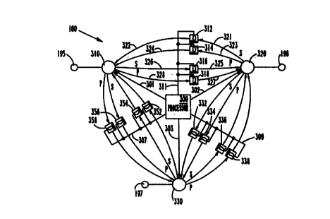
A preferred embodiment of the invention is now described with reference to the
three
electrode system shown in Figure 3. Referring to Figure 3, the pacemaker
system 100 preferably
includes three electrodes 195, 196, 197. In addition, the pacemaker system
includes node logic units
(or simply "nodes") 310, 320, and 330 coupled to electrodes 195, 196, 197.
Each pair of nodes is
interconnected by four communication paths; each communication path including
a delay module.
Each delay module delays a signal from one node to the next. Each node 310,
320, 330 preferably
CA 02304761 2000-02-17
WO 99/08747 PCT/US98/16735
-6-
provides one sense output signal S and one pace output signal P to the other
two nodes in the system
(for sake of clarity each sense and pace output signal is shown in Figure 3 as
two output signals).
The sense signal may be a digital signal that is asserted by a node upon
detection of electrical activity
at the electrode. The sense signal thus is asserted when the heart chamber
contracts in which the
electrode is implanted. The node may also provide pacing energy to the heart
via the electrode. The
pace output signal P is asserted by a node when the node paces the heart. The
pace output signal
P preferably is a digital signal that indicates when the chamber is paced.
Accordingly, node 320 provides a sense output signal on line 321 to delay
module 312 and
a pace output signal on line 323 to delay module 314. The delayed output
signals from delay
modules 312 and 314 are provided as input signals to node 310. Accordingly,
the input signals to
node 310 from delay modules 312 and 314 are provided on lines 322 and 324.
Similarly, node 310
provides a sense output signal on line 326 to delay module 316 and a pace
output signal on line 328
to delay module 318. The delayed output signals from delay modules 316, 318
are provided to node
320 via lines 325 and 327, respectively.
Sense and pace signals between nodes 310 and 330 and nodes 320 and 330 are
provided in
substantially the same manner for nodes 310 and 320. Accordingly, delay module
352 delays a sense
output signal from node 330 to a delayed sense input signal to node 310. Delay
module 354 delays
a pace output signal from node 330 to a delayed pace input signal to node 310.
Delay module 356
delays a sense output signal from node 310 to a delayed sense input signal at
node 330, and delay
module 358 delays a pace output signal from node 310 to a delayed pace input
signal at node 330.
Delay modules 332, 334, 336, and 338 similarly interconnect sense and pace
signals between nodes
320 and 330.
The pacemaker system shown in Figure 3 also includes a processor 300 which
controls the
amount of delay in each of the delay modules interconnecting the nodes 310,
320 and 330. Thus,
processor 300 controls delay modules 312, 314, 316, 318 via control signals on
lines 311. Processor
300 also controls delay modules 352, 354, 356, and 358 via control signals on
lines 307 and delay
modules 332, 334, 336, 338 via control signals on lines 309. Further, the
processor controls the
operation of nodes 310, 320, and 330 via lines 301, 302, and 303.
In accordance with the preferred embodiment in Figure 3, the time delay
associated with
each delay module is independently controlled by processor 300 and can be
programmed by external
programmer 400 (Figure 2). The architecture can easily be extended to include
four or five nodes,
or any other desired number of nodes. It should be recognized that as the
number of nodes
increases, so does the number of edges connecting the nodes. Examples of four
node systems are
discussed below with reference to Figures 10 and 12.
Each node 310, 320, 330 in Figure 3 preferably includes the same logic and
will be
CA 02304761 2000-02-17
WO 99/08747 PGT/US98/16735
_'7_
described with reference to node 310. Referring now to Figure 4, node 310
generally includes an
output amplifier 240, a sense amplifier 245, a node control and pulse
generator 250, pace output
logic 258, sense output logic 259, and delay modules 242, 244, 246, 248. The
node circuitry
preferably is implemented in an electronic assembly included within the
pacemaker housing. The
node control and pulse generator 250 provides a pacing signal on line 253 to
output amplifier 240.
The output amplifier 240 amplifies the pacing signal on line 253 and generates
an appropriate output
pacing signal on line 251 to electrode 195 coupled to node 310. The magnitude
and time duration
of the pacing signal from output amplifier 240 on line 251 is programmed into
the node control and
pulse generator 250 in accordance with known pacemaker protocol techniques.
The sense amplifier
245 amplifies the voltage on line 251 from the electrode and provides an
amplified version of the
electrode signal on output line 252. The output amplifier 240 and sense
amplifier 245 preferably are
low power amplifiers that amplify an analog input signal and produce analog
output signals. Thus,
output amplifier 240 provides pacing energy to the heart via an electrode and
sense amplifier 245
senses the electrical signal from the heart at the site of the electrode.
The pace output logic 258 preferably receives the analog pacing signal on line
251 from
output amplifier 240 and generates a pace output signal indicative of a paced
event on line 261.
Similarly, the sense output logic 259 receives the analog output signal from
sense amplifier 245 via
line 252 and generates a sense output signal on line 262 indicative of a
sensed event. The pace and
sense output signals preferably include a digital value or other signal to
indicate that a paced and
sensed event has occurred.
In addition to delay modules between nodes (Figure 3), each node preferably
includes delay
modules 242, 244, 246, and 248 to provide various delays to signals within the
node. The delay
time associated with each delay module is programmable in processor 300 via
control lines 239.
Delay module 242 provides the sense output signal from the sense output logic
259, following a time
delay, to the output amplifier 240 as a control signal on line 243. Similarly,
the delay module 244
provides the pace output signal from the pace output logic 258, following a
time delay, as a control
input signal on line 241 to the output amplifier 240. Further, following a
delay, the delay module
246 provides the sense output signal from the sense output logic 259 as a
control signal to the sense
amplifier 245 via line 247. Finally, delay module 248 provides the pace output
signal from the pace
output logic 258 as a control input signal on line 249 to the sense amplifier
245. The control signals
to the amplifiers 240, 245 on lines 241, 243, 247, 249 control the operation
of the amplifiers.
Specifically, the control signals can be asserted to inhibit the output
amplifier 240 from emitting a
pacing signal to the electrode and inhibit the sense amplifier 245 from
sensing the voltage from the
electrode. Alternatively, the control signals on lines 241, 243 can be
provided to the node control
and pulse generator 250, instead of the output amplifier, to inhibit the node
control and pulse
*rB
CA 02304761 2000-02-17
WO 99/08747 PCT/US98/16735
_g_
generator 250 from providing an input pacing signal on line 253 to the output
amplifier 240.
Further, the sense amplifier control signals on lines 247, 249 can be provided
to the sense output
logic 259, rather than the sense amplifier, to inhibit the sense output logic
259 from producing a
sense output pulse on line 262.
The node logic described above advantageously allows the node's pacing
function to be
controlled by both paced and sensed events associated with the node. For
example, the output
amplifier 240 provides a pacing signal to the electrode in response either to
a paced event or sensed
event via control signals on lines 241 and 243, respectively. Further, delay
module 244 allows the
node 310 to produce a pacing signal to the electrode after a time delay
following a paced event.
Similarly, delay module 242 allows the node 310 to produce a pacing signal
after a time delay
following a sensed event. The length of delay following a paced or sensed
event before a pacing
signal is provided to the electrode is controlled independently for each delay
module 242, 244 by a
processor (Figure 3) via control lines 239 which are represented in Figure 3
as control lines 301,
302; and 303.
The logic of node 310 also provides for full control over the node's sensing
function. Thus,
the sense amplifier 245 is triggered to detect sensed events following either
a paced or sensed event
via delay modules 248 and 246, respectively. Sensing may be triggered upon
detection of a sensed
event by sense output logic 259 after a delay as determined by delay module
246. Alternatively or
in addition to, sensing may also be activated upon detection of a paced event
following a delay as
determined by delay module 248. As for delay modules 242 and 244, the delay
times associated with
delay modules 246, 248 are independently controlled via signals on control
lines 239.
The sense and pace output signals from all other nodes are provided as input
signals via lines
257 and 256, respectively, to the node control and pulse generator 250. The
node control and pulse
generator preferably responds to one or more of the sense and pace input
signals on lines 256, 257
by providing control signals on lines 254 and 255 to the output amplifier 240
and sense amplifier
245. These control signals, like the control signals on lines 241, 243, 247,
249, inhibit the pacing
and sensing functions of the node. Rather than controlling sense amplifier
245, control signal 255
alternatively may be provided to the sense output logic as described above
with respect to the control
signals on lines 247, 249. Additionally, instead of providing a control signal
on line 254 to the
output amplifier 240, node control and pulse generator 250 instead may inhibit
pacing by simply not
providing an input pacing signal to the output amplifier on line 253. Thus,
the universal architecture
of the preferred embodiment of the invention allows the pacing and sensing
activity of one node to
be controlled by paced and sensed events associated with any other node in the
system.
The preferred embodiment of pacemaker 100 illustrated in Figure 3 is a three
node (three
electrode) system. Alternatively, pacemaker 100 can be configured with
different numbers of
CA 02304761 2000-02-17
WO 99/08747 PCT/US98/16735
-9-
electrodes. In Figure 5, a two node system includes nodes 160, 165 coupled to
electrodes 183, 184.
Each node preferably provides a pace and a sense signal to the other node by
way of communication
paths 161, 163. Each communication path preferably includes a programmable
delay module (not
shown for sake of simplicity). By way of an additional example, a four node
system is shown in
Figure 6 and includes nodes 190, 200, 210, 220 coupled to electrodes 185, 186,
187, 188
respectively. Each node provides pace and sense signals to all other nodes via
communication paths
191, 193, 194, 196, 198, 201, 203, 205, 207, 209, 212, and 214.
The pacemaker system of Figure 3 includes a separate delay module for each
pace and sense
signal provided between pairs of nodes. Figures 7 and 8 include alternative
embodiments in which
a single delay module can be used to replace two delay modules. In Figure 7 a
single delay module
is used to provide a delay for signals passing in opposite directions between
two nodes. In Figure
8, a single delay is used to provide a delay for pace and sense signals
provided from one node to
another node in the same direction.
Referring first to Figure 7, a single delay module 230 delays the sense output
signals from
IS each of the nodes 310 and 320. A switch 335, under control by processor 300
via control line 333,
connects the delay module 230 to the nodes to delay each node's sense signal.
The switch 335
preferably is configured as a double pole, double throw switch and includes
two switches 336, 337
as shown. Each switch 336, 337 includes a pole 336a, 337a and two contacts. As
is commonly
known for a double pole, double throw switch, all switches it contains are
forced to the same state.
That is, the poles 336a, 337a in switches 336, 337 will couple to the
comparable contacts in each
switch; either in the state shown in Figure 7 or in the alternative state
indicated by the dashed lines
between the pales and the lower contact shown.
With switches 336, 337 in the state shown in Figure 7, the sense signal from
node 320 on
line 321 is delayed by delay module 230 and provided as a delayed sense signal
on line 322 to node
310. The sense signal on line 321 conducts through switch 336, line 342, delay
module 230, line
343, switch 337, and line 322 to node 310. By asserting the control signal on
line 333, processor
300 can command the double pole, double throw switch 335 to the alternative
state shown by the
dashed lines in switches 336 and 337. Once switches 336, 337 are switched to
the alternative state,
the sense signal from node 310 on line 326 conducts through switch 336, line
342, delay module
230, line 343, switch 337, and line 325 to node 320.
The switching arrangement in Figure 7 does not permit the delay module 230 to
delay both
sense signals simultaneously. Therefore, the arrangement of Figure 7 may not
be preferred if it is
possible for both sense signals to be asserted simultaneously. Simultaneously
detected sense events
generally do not occur, however, because the electrodes associated with the
nodes are implanted in
different locations in the heart and it takes a finite amount of time for an
electrical signal to propagate
CA 02304761 2000-02-17
WO 99/08747 PCT/US98/16735
-10-
through the tissues of the heart from one electrode to another. Thus, two
electrodes will generally
not simultaneously register a sensed event resulting from a common electrical
signal propagating
through the heart.
Referring still to Figure 7, to provide added flexibility the processor can
program the delay
module 230, via control line 311, to provide different time delays for each of
the sense signals.
Moreover, the switch and delay module configuration in Figure 7 can be used to
delay any pair of
signals transmitted in opposite directions between nodes and independently
control the amount of
delay associated with each signal.
Referring now to Figure 8, a single delay module can also be used to delay
pace and sense
signals conducted in the same direction between a pair of nodes. Switch 390
preferably includes a
double pole, double throw switch, and accordingly includes switches 391 and
392. Like switches
336, 337 in Figure 7, switches 391, 392 are controlled in tandem by a control
signal on line 393
from processor 300. With switches 391, 392 in the state shown in Figure 8, the
sense signal from
node 310 on line 326 is provided to node 320 via switch 391, delay module 230,
switch 392 and line
325. Via the control signal on line 393 to switches 391, 392, processor 300
can command switches
391, 392 to the alternative state shown by the dashed-lines in the switches.
Once in the alternative
state, the pace signal from node 310 on line 328 is provided to node 320 via
switch 391, delay
module 230, switch 392, and line 327. Further, processor 300 can program delay
module 230 to
have a different delay for the sense signal on line 326 as compared to the
delay desired for the pace
signal on line 328. Additionally, it should be recognized that additional
switches can be added to
allow a single delay module to be shared by more than two signals.
The embodiment shown in Figure 7 allows delay reversal for signals conducting
between
nodes in opposite directions. The embodiment of Figure 8 allows a single delay
module to be shared
between nodes for at least two signals passing in the same direction between
nodes. Referring now
to Figure 9, both delay module reversal and delay module sharing are shown
using switches 365,
367 to pace and sense signals between nodes 310 and 320. Switch 365 includes
switches 373 and
374 and allows delay module 230 to be reversed, similar to switch 335 in
Figure 7, thereby delaying
pace and sense signals in either direction between nodes 310 and 320. The
state of switch 365 is
determined by a control signal on line 311 from processor 300. Switch 367 is a
two pole, four throw
switch including switches 371 and 372 which are controlled in tandem by a
control signal on line 377
from processor 300. Processor 300 independently controls switches 365, 367 by
asserting control
signals on lines 376, 377. As shown in Figure 9, delay module 230 with
switches 365, 367 can be
used to replace the four delay modules 312, 314, 316, 318 between nodes 310
and 320 of Figure 3.
With the state of switches 367, 365 as shown in Figure 9 (i.e., pole 371b
connected to
contact 371a, pole 372b connected to contact 372a, and poles 373a, 374a
connected to contacts 373b
CA 02304761 2000-02-17
WO 99/08747 PCT/US98/16735
-11-
and 374b, respectively), the sense signal from node 320 on line 321 is
provided to node 310. The
conducting path for the.sense signal from node 320 includes line 321, switch
372, switch 373, delay
module 230, switch 374, switch 371 and line 322. The pace signal from node 320
conducts along
a similar path once switches 371 and 372 are switched to the state in which
the poles 371a and 372a
connect to contacts 371c and 372c.
The sense and pace signals from node 310 are provided to node 320 in a reverse
direction
by changing the state of switches 373 and 374 to the alternate state in which
poles 373a and 374a
connect to contacts 373c and 374c. The sense signal from node 310 conducts
along a path including
switch 371 (with its pole 371a connected to contact 371d), switch 365, delay
module 230, switch
374, switch 372, and line 325. The pace signal from node 310 follows a similar
path after processor
300 directs switches 371 and 372 to change states so that poles 371a and 372a
connect to contacts
371e and 372e, respectively. Additionally, processor 300 preferably programs
delay module 230
to provide the desired delay for each sense and pace signal.
Thus, the many individual delays represented by the edges and nodes of the
multi-site
pacemaker, in accordance with the preferred embodiment, may be reduced to
fewer delay modules,
as desired. The switches in Figures 7-9 preferably include electronic switches
constructed of low
power CMOS or other integrated circuit technologies. Although depicted as
discrete elements in
Figures 3-4, 7-9, the delay modules may alternatively be implemented in
software by the processor
300, as would be known by those of ordinary skill in the art.
The description of the preferred embodiment discussed above represents a
universal
architecture for implantable medical devices such as pacemakers. The time
delay associated with
all of the delay modules shown in Figures 3-4, 7-9 preferably are programmable
via control signal
inputs from processor 300. Further, any time delay may be programmed to a
value of 0 (i.e., no
delay) or to any other value. The pacemaker configuration of Figure 3 is
completely connected
in that all pairs of nodes are connected by communication paths. It may be
desired, however, to
configure a pacemaker system that is not completely connected (i.e., some
pairs of node are not
connected by communication paths). Thus, the pacemaker 100 preferably can be
configured to either
provide a delay path between a pair of nodes, or not, as desired. Being able
to configure the
pacemaker's communication paths in any manner desired allows the pacemaker to
provide a wide
variety of pacemaker therapies, when previously multiple pacemakers were
required to provide the
desired therapies. One technique for indicating no connection is to be made
between a particular pair
of nodes is to program the delay modules) associated with the pair of nodes to
a value that is defined
to mean no connection is desired. For example, a delay time of 100 seconds may
be used to indicate
that no connection is needed.
Thus, given a set of implanted electrodes coupled to a pacemaker, any
configuration such
CA 02304761 2000-02-17
WO 99/0874? PCTNS98/16735
-12-
as those shown and discussed above is possible. The configuration desired can
be programmed
during implantation of the pacemaker or programmed in a post surgical follow-
up visit using the
external programmer 400 shown in Figure 2. In accordance with the preferred
embodiment, the
external programmer 400 receives configuration data from the implanted
pacemaker reflecting the
particular configuration in which the pacemaker currently is operating.
Programmer 400 may
download a new configuration data set to the pacemaker to program the
pacemaker to a new
configuration. Many techniques are possible for encoding the configuration bf
the pacemaker, a few
of which are discussed below with reference to Figures 10-13.
Referring now to Figure 10, a four node system includes nodes for the right
atrial electrode
(RA), right ventricular electrode (RV), left atrial electrode (LA), and left
ventricular electrode (LV).
The configuration shown in Figure 10 corresponds to a four-chamber pacemaker
with one electrode
in each of the chambers of the heart. Referring still to Figure 10, the RA
node provides pace and
sense signals via delay modules 401, 402, 405, 406, 411, and 412 to the LA,
RV, and LV nodes.
Similarly, the LA node provides pace and sense signals via delay modules 403,
404, 407, 408, 409,
and 410 to the RA, RV, and LV nodes.
Referring to Figure 1 l, the configuration of Figure 10 is shown in tabular
form in which "P"
signifies that a connection provides a pace output signal to be transmitted
between the nodes indicated
and "S" signifies that a connection provides a sense output signal between the
nodes. The blanks
in the table of Figure 11 indicate that there is no connection between the
associated pair of nodes.
As such, the table of Figure 11 reflects the linear graph configuration for
the pacemaker system of
Figure 10. It should be recognized that additional information may be
necessary to fully configure
a pacemaker. Such additional information generally includes the time delay
values associated with
each delay module, the sense amplifier sensitivity, pulse amplitudes and
widths of the output pulses
to the electrodes, the bandwidth of the sense amplifiers, and other variables
not reflected in the table
of Figure 11 but which can be provided to programmer 400 via known techniques.
By way of an additional example, Figure 12 represents a four vode pacemaker
system and
Figure 13 includes the associated configuration table in accordance with the
technique described
above with respect to the configuration table of Figure 11. Referring to
Figure 12, the configuration
shown includes one electrode in the right atrium (represented as the RA node)
and three more
electrodes in the right ventricle and represented as nodes RV1, RV2, and RV3.
The configuration
of Figure 12 represents a two-chamber, four-site pacemaker. The RA mode
provides pace and sense
output signals via delay modules 420 and 421 to the RV 1 node which, in turn,
provides pace and
sense output signals via delay modules 422 and 423 to the RV2 node. The RV2
node provides only
a pace output signal to the RV3 node via a delay module 424.
Once the external programmer 400 receives the configuration of the implanted
pacemaker,
CA 02304761 2000-02-17
WO 99/0874? PCT/US98116?35
-13-
a new configuration may be established for the implanted pacemaker.
Accordingly, the implanted
pacemaker can be reconfigured by downloading a new configuration table from
the programmer to
the implanted device (provided the electrodes are in the desired locations).
Further, the external
programmer may display the configuration information.