Note: Descriptions are shown in the official language in which they were submitted.
CA 02305069 2000-04-12
MICROMACHINED ELEMENT AND METHOD OF
FABRICATION THEREOF
The present invention relates to micromachined systems and elements generally
and,
5 more particularly, but not by way of limitation, to microsensors,
microactuators,
microprobes, and probe cards and, more particularly, but not by way of
limitation, to a
novel micromachined coiled element and method of fabrication thereof.
Various micromachined or microelectromechanical devices, such as sensors and
10 actuators, on a microscopic scale have been developed.
For example, U.S. Patent No. 5,434,513 issued to Fujii et al. discloses a
semiconductor wafer testing apparatus capable of allowing numerous circuit
elements
of a semiconductor wafer to be tested at once. A plurality of pogo pins which
have
moveable connection pins inserted therein. are urged downward and are moveable
in
15 an axial direction, wherein the tips of the respective connection pins
contact the
pickup electrodes or control electrodes formed on the semiconductor wafer,
with
pressure, to provide electrical connections.
U.S. Patent No. 5,172,050 issued to Swapp discloses a probe fixture for
testing an
integrated circuit, the probe fixture including a semiconductor substrate, a
plurality of
20 cavities etched into the substrate, a plurality of flexible beams formed
from the
substrate, wherein each beam extends over a portion of each of the cavities, a
plurality
of conductive probe tips, wherein each probe tip is formed on one of the
beams, and a
conductive interconnect formed on the substrate for coupling each probe tip to
an
external circuit tester. The electrode pads are forced into contact with the
probe tips
25 when the semiconductor probe card and integrated circuit are pressed firmly
together.
CA 02305069 2000-04-12
U.S. Patent No. 4,520,314 issued to Asch et al. discloses a test probe head
for
contacting and testing a plurality of exposed closely spaced electrically
conductive
members of very small dimensions, wherein the probe comprises a monolithic
monocrystalline silicon comb-shaped structure having a spine portion and a
plurality
of elongated teeth which provide a plurality of miniature resilient cantilever
beams.
U.S. Patent No. 5, 415,555 issued to Sobhani discloses an electrical
interconnection
apparatus which utilizes raised.connecting means. A pair of electrical
circuits, which
may be both flexible, or one flexible and one rigid, are interconnected by
projections,
such as bumps or rings.
10 U.S. Patent No. 5,012,187 issued to Littlebury. teaches a method of testing
integrated
circuits using a tester which is capable of testing a plurality of memories in
parallel.
A membrane test head having a plurality of probe bumps is coupled to the
tester.
U.S. Patent No. 5,510,721 issued to Walles et al. discloses a test socket for
testing an
integrated circuit, wherein a substrate has a plurality of trenches that are
traversed by a
15 plurality of resilient conductive straps which extend across the trenches.
The straps
are deformed in a predetermined manner into the trenches while the straps are
urged
against the contacts.
Patent No. EP 687 907 issued to Hamasaki discloses a microeddy current sensor
having a coil formed on a silicon substrate by a micromachining technique
wherein
20 the coil is formed ~by electrode deposition of a metal. The coil has a
multiiayered
structure in the vertical direction and/or a core formed proximate the central
position
of the coil. A resist layer is formed on a silicon substrate through an
insulating film
by micromachining, and a spiral groove is two-dimensionally formed in the
resist
layer by patterning, whereafter a metal such as copper is buried in the groove
by
25 electrodeposition. thereby forming a coil. resulting in a microeddy current
sensor
which can detect a small change in magnetic field.
CA 02305069 2000-04-12
.3.:
U.S. Patent No. 4,740,410 issued to Muller et al. discloses a method, and the
product
resulting therefrom. for making a microminiature structure with two or more
members
which are relatively moveable to each other, such as a spring-restrained pin
joint. A
spiral spring extends through two and half revolutions and is made of two
5 micrometer-wide second-layer polysilicon. The central end of the spring is
connected
to a hub, and the outer end is connected to a moveable arm. The horizontal
spring
structure is used in ratchet closures and brush-contact detents.
Patent No. WO 96/24145 issued to Ho discloses a micromachined micromagnetic
actuator having a flap capable of large deflections using a magnetic actuating
force.
10 The flap is coupled by one or more beams to a substrate, and is
cantilevered over the
substrate. A magnetic layer or magnetic coil is disposed on the flap, wherein
the flap
is selectively rotated out of the plane of the substrate. The flap comprises
different
layers, and the intrinsic stresses of the different layers contribute to a
bending moment
which causes the flap to be curved, rather than flat, at rest. Thermal
mismatch of
15 different materials in the composite layers causes the flap to bend down.
The motion
of the flap is a result of both thermal and magnetic effects. The patent also
discloses a
method of fabricating the microelectromagnetic actuator, wherein the method
comprises providing a substantially completed actuator on a sacrificial layer
disposed
on an underlying substrate, removing the sacrificial layer by etching away
through at
20 least one opening defined through the actuator to expose the underlying
sacrificial
layer, and drying the actuator while simultaneously actuating the actuator to
maintain
the released portions of the actuator out of contact with the underlying
substrate until
the drying is complete.
Many of the techniques used in silicon chip processing have been used to
produce
25 these devices. The techniques include photolithography, x-ray and beam
lithography,
layer deposition and etching techniques.
Wafer probe cards may incorporate an array of elements for device
characterization.
Various elements such as cantilevers and probes of various shapes, structures,
CA 02305069 2000-04-12
-4-
compositions, and membrane probe card structures have been developed for
testing of
semiconductor chips.
U.S. Patent No. 5,475,318 issued to Marcus et al. discloses a microprobe
comprising a
bimorph actuated microcantilever having a probe tip which projects from the
5 microcantilever. Upon heating of the microcantilever, the probe tip comes
into
contact with a material to be investigated.
Wafer-stage testing of semiconductor chips is pervasive throughout the
industry. As
chips get larger and more complex, such testing becomes increasingly difficult
to
execute with existing probe/test technology. As chips get more complex, the
various
10 components became smaller, their numbers increase, and the number of I-O
pads on a
device increases. Testing becomes even more difficult where contact surfaces
are
non-planar, such as encountered with solder bumps, curved "smart skin"
surfaces, or
in ~multi-chip assemblies.
Known membrane probes consist of an arrangement of probe contact pads on a
15 membrane which are made to contact the device pads by applying a small
pressure,
forcing the two together. Although membrane probe card technology might be
used
for probing and testing the next generation of chips and packages, various
problems
inherent with the membrane probe card exist, as related, for example, to the
increasing
size of the membrane required for larger chips (in order to reduce the effect
of
20 bowing), the inability of the membrane probe card to offer compliant
contact with
surfaces of varying height as with the components of a Multi-Chip-Module
(MCM),
and the overall difficulty of using a membrane technology compared with a
technology based on a rigid surface, such as a surface based upon silicon.
Therefore, the need exists, and continues to grow, for contacting circuits on
wafers
25 having varying heights or nonuniform surfaces for purposes of testing
and/or
connection with, or interconnection between, circuit elements during
operation.
CA 02305069 2000-04-12
-5-
Accordingly, it is an object of the present invention to provide a microprobe
which
has a built-in compliancy for contacting adjacent surfaces of varying heights.
Such a
feature is absent from existing membrane probe cards.
It is another object of the present invention to provide a microprobe which
applies a
5 force to a contact pad wherein the force increases superlinearly as pressure
is
increased. Such feature is missing from existing cantilever contacts.
If is a further object of the present invention to provide a microprobe such
that the
probe card nominal surface is~preferably planar, not curved, thereby
permitting larger
structures to be probed as compared to structures which are testable by
existing probe
10 membrane cards.
It is yet another object of the present invention to incorporate a plurality
of
microprobes into an integrated probe card for wafer-stage probing or testing
of device
chips and for pmbing or testing of mufti-chip assemblies.
It is another object of the present invention to provide a process for making
such a
15 microprobe.
It is still another object of the present invention to provide a probe card
having a high
pad density.
It is yet another object of the present invention to provide a probe card
which can
contact area arrays as well as perimeter arrays.
20 It is a further objecnof the present invention to provide a probe card
having a high
density of surface contacts.
CA 02305069 2000-04-12
~6y
These and other objects are achieved by means of the present invention which
provides. in at least one embodiment, a micromachined element mounted to a
substrate, wherein the micromachined element comprises a cantilever having a
proximal portion attached to the substrate and a free distal end, wherein the
cantilever,
upon being heated. is capable of bending away from the substrate and at least
partially
coiling upon itself to define a distal coiled portion.
In another embodiment, the present invention relates to a micromachined
element
mounted to a substrate, wherein the micromachined element comprises a
cantilever
having a proximal portion attached to the substrate and a coilable distal
portion
terminating in a free distal end. The coilable distal portion, upon being
heated, is
capable of bending away from the substrate and at least partially coiling upon
itself to
form a coiled portion. Heat may be applied globally to the cantilever. or
group of
cantilevers, to form the coiled portion(s), or heat may be resistively
generated within
each cantilever to form the coiled portion.
The free distal end may follow an inward spiral path when heat is supplied to
the
cantilever. Preferably, the degree of bending in the cantilever increases in a
distal
direction. The radius of curvature of the coiled portion preferably decreases
distally
along the cantilever.
The cantilever is preferably permanently suspended over the substrate and is
separated
therefrom by a gap.
The cantilever may either reversibly or irreversibly coil upon itself,
depending, for
example. upon the material from which the microelement is constructed.
At least part of the cantilever may be electrically conductive.
CA 02305069 2000-04-12
_7.
Moreover, at least part of the coiled portion may be electrically conductive,
whereby
electrification of the conductive part of the coiled portion generates an
electromagnetic field. Thus, the micromachined element may be capable of
generating a magnetic field, e.g. a field having an axis generally parallel to
the surface
of the substrate from which the element extends.
The cantilever may be electrically insulated from the substrate.
Preferably, the coiled portion is capable of being resiliently compressed.
In a preferred embodiment, the cantilever is substantially comprised of a
bimorph
structure or bimorph material construction.
Thus, the cantilever may further comprises a first conducting layer having at
least one
portion disposed proximate the substrate and a second layer disposed over the
inner
first conducting layer.
The cantilever may further include a conductive lead attached to the first
conducting
layer.
I S In a particular embodiment, the cantilever may include a first conductive
lead attached
to the first conducting layer proximate the proximal portion and a second
conductive
lead attached to the first conducting layer proximate the free distal end,
whereby the
coiled portion is capable of being electrified, thereby generating a magnetic
field.
The first layer has a greater coefficient of thermal expansion than the second
layer. In
a particular embodiment, the first layer is comprised of a metal.
The cantilever may be at least partially voluted. The cantilever may further
include at
least one volute. For example, the cantilever may include at least one outer
volute and
at least part of an inner volute. The outer volute may be spaced apart from
the inner
CA 02305069 2000-04-12
_$_
volute when the micromachined element is uncompressed. At least two adjacent
the
volutes may be capable of resiliently contacting one another when the
micromachined
element is compressively loaded.
Thus, the volutes may be spaced apart from each other when the element is
uncompressed. The outer volute may compress before the inner volute when the
micromachined element is compressively loaded.
By way of further example, the cantilever include a plurality of volutes.
In another aspect, the present invention relates to a method of fabricating a
coilable
microelement upon a substrate, the method comprising the following steps:
depositing
a sacrificial layer upon the substrate; depositing and patterning resist
thereby defining
at least one metal reception region; depositing a first layer of a first
material on the at
least one metal reception region; depositing a second layer of a second
material on top
of the first layer, wherein the first layer has a higher coefficient of
thermal expansion
than the second layer; removing the resist; removing the sacrificial layer,
thereby
freeing at least one cantilever; and heating the at least one freed
cantilever, thereby
causing the at least one freed cantilever to at least partially curl upon
itself. An
underlying insulating layer may first be deposited upon the substrate.
Further, a metal
ground plane may be deposited upon the sacrificial layer before depositing and
patterning the resist, wherein the first layer is electrodeposited atop the
metal ground
plane.
The method may further comprise attaching at least one heater to at least one
of the
freed cantilevers. Alternatively, or in addition, the microelement may be
globally
heated to cause the at least one freed cantilever to at least partially curl
upon itself.
In another embodiment, a method of fabricating a coiled microelement upon a
2~ substrate, according to the present invention, comprises the following
steps:
depositing an insulating layer upon the substrate; depositing a sacrificial
layer upon
CA 02305069 2000-04-12
_9,
the insulating layer; patterning the sacrificial layer, thereby forming at
least one
remaining strip of sacrificial layer; depositing a metal ground plane upon at
least a
portion of the exposed insulating layer; depositing and patterning resist
thereby
defining at least one metal reception region to expose at least a portion of
the ground
5 plane; electrodepositing a first layer of metal on the at least one metal
reception region
and the resist; depositing a layer of a second material on top of the first
layer wherein
the first layer has a higher coefficient of thermal expansion than the second
layer;
removing the resist such that the second layer is patterned by lift-off;
removing the
remaining sacrificial layer so as to free at least one cantilever; and heating
the freed
cantilever, thereby causing the freed cantilever to at least partially curl
upon itself.
The substrate may be comprised of silicon. The insulating layer may be
comprised of
an oxide.
The method may further include the subsequent step of electroplating the
exposed
surface of the first layer with a conductive material.
I 5 The cantilever may be individually or globally heated, or both.
Understanding of the present invention and the various aspects thereof will be
facilitated by reference to the accompanying drawing figures, submitted for
purposes
of illustration only and not intended to limit the scope of the invention, in
which:
Figure 1 is a scanning electron microscope (SEM) photograph showing the basic
structure of one embodiment of a micromachined element according to the
present
invention;
Figure 2 schematically illustrates a side elevational cut-away view of a
microspring
according to the present invention;
CA 02305069 2000-04-12
10-
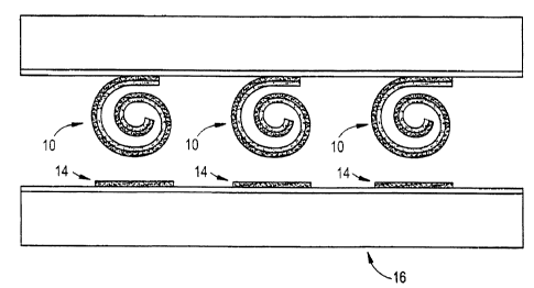
Figure 3 illustrates a side elevational cut-away view of part of an array of
microsprings on a probe card according to the present invention;
Figure 4 schematically illustrates, the compression of a microspring according
to the
present invention mounted on a substrate during ohmic contact with a contact
pad of a
device-under-test;
Figures 5-7 scHematically illustrate successive compression of a microspring
according to the present invention;
Figure 5 shows the microspring under a slight applied force;
Figure 6 shows the microspring under an applied force which is stronger than
that of
Figure 5:
Figure 7 shows an even stronger force applied to the microspring than in
Figures 5
and 6;
Figure 8 is a side elevational view of a microspring or microcoil precursor
according
to the prescnt invention;
I 5 Figure 9 is a side eievational view of a microspring or microcoil
according to the
present invention which results from the precursor of Figure 8 after the
application of
heat;
Figure 10 illustrates a side elevational cut-away view of another embodiment
of the
present invention;
Figure 11 shows a side elevational cut-away view of yet another embodiment of
the
present invention;
CA 02305069 2000-04-12
-I1-
Figure 12 schematically represents one embodiment of a layout of cantilevers
which
are precursors for microsprings according to the present invention;
Figure 13 shows the results of forming the precursors of Figure 12 into
microsprings
or microcoils to provide an array according to the present invention;
S Figure 14 is a plan view of a CHIPP probe card having cantilevers for
contacting a
perimeter array of pads on a chip, wherein the microsprings of the present
invention
vrould replace the cantilevers;
Figure 15 is a graphically representation of the calculated deflection of a
microspring
according to the present invention at three different temperatures;
Figure 16 schematically illustrates the deflection response to an applied
force on a
microspring element according to the present invention;
Figure 17 is a side elevational cut-away representation of another embodiment
of the
present invention showing a bimorph structure suitable for global heating;
Figures 18-20 illustrate a series of processing steps which may be used to
produce the
microspring or microcoil structure according to the present invention;
Figure 18 is a side elevational cut-away view of a microspring or micmcoil
precursor;
Figure 19 is a side elevational cut-away view of a microspring or microcoil
formed
from the precursor of Figure 18;
Figure 20 is a side elevational cut-away representation of the microcoil or
microspring
of Figure 19 wherein the outer or exposed surface of the inner layer of the
bimorph
structure is plated;
CA 02305069 2000-04-12
12-
Figure 21 is a side elevational cut-away view of a precursor to yet another
embodiment of the present invention which is capable of producing an
electromagnetic field; and
Figure 22 is a perspective view of the microcoil formed after heating the
precursor of
5 Figure 21.
Figure 1 is a scanning electron microscope (SEM) photograph showing the basic
structure of one embodiment of a micromachined element which can serve as a
microprobe, according to the present invention. Figure 1 shows a microelement
or a
10 microspring made of 40 pm-wide thin film slab consisting of metal and oxide
layers
at a magnification of 500X. The microelement shown may be characterized as a
coil
or a spring which is made from a cantilever member. Thus, each microprobe may
be
a microspring or microcoil. The proximal end of the microcoil projects
outwardly
from a base area and is preferably curled upon itself such that the distal end
of the
I S microcoil is surrounded by at least part of a volute, or a convolution. or
tum of the
microcoil.
As further explained below, the application of heat in form of electric
resistance
heating caused by a current passed through a cantilever made of substrate
material, or
by proper application of global heating such as furnace heating causes the
cantilever
20 to bend and coil upon itself. Preferably, the curling effect is
irreversibly manifested
by inducing a temperature high enough to plastically deform the cantilever.
On the other hand, the curling may be effected elastically or reversibly. For
example
if each cantilever is individually heated for example by resistive heaters, a
microspring probe card according to the present invention can be heated to
curl one or
25 ~ more microsprings, can make temporary contact with a device to be tested,
then
removed, after which heating power to the microsprings is terminated, causing
the
CA 02305069 2000-04-12
-13=
springs) to flatten back into a cantilever orientation. That is, a generic
array of
cantilevers could be made, and individual levers actuated to form microsprings
wherever needed to provide contact.
Thus, an area contact array can be contacted by a probe card containing a
plurality of
microcoils which serve as contacts with the contact pads that are situated on
the array.
Preferably, each coil contact on a microprobe card comprises a plurality of
coils made
from stiff, elastic conductor material.
Figure 2 schematically illustrates a microspring or microcoil 10 according to
the
present invention with one part fixed to a surface of the substrate 12 of the
probe card,
which may be a silicon wafer. The microspring 10 is electrically isolated from
the
substrate by a thin insulating film 13. The fixed part would typically be
electrically
connected with broad pads at the edge of the probe card by IC technology known
by
those skilled in the art. The broad pads at the edge are configured to
facilitate
connections with standard plug contacts or connectors to external sources or
devices.
I 5 Figure 3 schematically illustrates part of an array of microsprings 10 on
a probe card
ready to make ohmic contact with pads I4 on a device-under-test 16.
Figure 4 schematically illustrates the compression of the microspring 10
mounted on
its substrate 12 during ohmic contact with the contact pad 14 of a device-
under-test
16. As the spacing between the wafer surface containing the microsprings 10
and the
wafer surface of the device-under-test 16 containing the contact pads 14
decreases, the
contact force increases superlinearly as additional spring elements or
portions coming
into play with increasing compression, as represented by Figures 5-7.
Figure 5 represents a microspring 10 under slight compression, for example due
to a
slight applied force. The load is first taken up by the right side of the
outermost coil
as denoted by the heavy line between F and the substrate surface.
CA 02305069 2000-04-12
-14-
Figure 6 represents the microspring under a stronger applied force, wherein
the
underside of the outermost coil contacts the substrate area. wherein the load
is taken
up by more of the microspring. for example the outermost volute.
Figure 7 represents the microspring under an even greater load which is taken
up by a
5 greater portion of the volutes.
Figures 8 and 9 show a side view of a microcoil precursor 20 and a resulting
microcoil
10, respectively.. In Figure 8, the sacrificial layer 22 was removed to a
distance "a"
from its edge before heating. After heating, the fully formed coil 10 has a
diameter
"2b".
10 Figure 10 schematically illustrates a cross-section of another embodiment
of the
present invention having a configuration which allows ohmic connection between
microsprings on one side of a wafer and an integrated circuit on the other
surface,
which contains interconnects, passive and active thin film devices, through
vial. This
"backplane" can be used to supply temporary and/or permanent connections
within a
15 chip. or temporary and/or permanent connections among chips and other
devices in a
mufti-chip assembly/module. Thus, the embodiment of Figure 10 may be an
"interconnection wafer" 30 having a microspring 10 on the second surface 32,
electrical connection through a via 34 to the first surface 36, and electrical
connections 38 to thin film interconnects and/or components on the first
surface 36.
20 In the particular embodiment shown in Figure 10, the metal element labeled
"p" on
the first surface 3b and electrically connected to the microspring 10 on the
second
surface 32 is available for connection to the n+ region MOS transistor or to
any other
device element or component on that surface.
Thus, Figure 10 shows an alternate connection means comprising openings or
vias 34
25 through the silicon layer to the back surface 36 of the wafer 30. As used
herein, the
term "via" refers to an opening in a layer provided to allow electrical
contact from one
surface to another through the opening.
CA 02305069 2000-04-12
-15-
Figure 11 shows yet another embodiment of the present invention wherein the
interconnects 38 are disposed on the same surface as the microcoil or
microspring 10.
As illustrated by the embodiment shown in Figure 11, an electrical connection
to each
of the spring contacts 10 could be achieved through a lower level of
metalization,
5 where the metalization layer 38 and the microsprings 10 are separated by a
thin
insulating layer 13 and electrical connection is made through vial 34 in the
insulating
layer 13. A wafer 30 may contain microsprings 10 and its own interconnections,
and
possibly also some active devices, such as FETs, capacitors, etc., which can
be made
on the same side of the wafer as the microsprings 10, as shown in Figure 11,
or, on the
10 opposite side where more room is available, as shown in Figure 10.
The cantilever element 20 from which the coil 10 is formed is preferably a
bimorph.
For example. as seen in Figure 8, an oxide 22 is sandwiched between a silicon
substrate 12 and the bimorph 20, wherein the oxide or sacrificial layer
portion 22 has
been removed in the area demarcated by "a". After heating, the bimorph 20
15 transforms into the microcoil 10, for example as shown in Figure 9,
resulting in a
radius labeled "b". In this example, the linear space needed to form a spring
of
diameter "2b" is "a".
Figure 12 represents one embodiment of a layout of cantilevers 20 which are
precursors for the microsprings. The cantilever length is "a" and the width is
"w" and
20 the spacing between cantilevers "s". The interconnections to the
cantilevers are not
shown.
Figure 13 shows the results of forming the precursors 20 into microsprings 10
thereby
providing an array of (a + s) by (w + s).
Most device chips made in the past have had contact pads arranged around the
25 perimeter of the chip ("perimeter array"), and new device chips have pads
located in
CA 02305069 2000-04-12
- l6-
the interior of the chip ("area array") or have a combination of interior and
perimeter
arrays.
As shown in Figures 12 and 13, an area array of cantilever members 20 has a
length
"a" longitudinally separated by distance "s" and has a width "w", wherein the
5 cantilevers 20 are transversely separated by distance "s". After heating.
the coils 10
are formed so as to provide contacts which are longitudinally separated by the
distance "a+s". and transversely separated by the distance "w+s". Thus, the
area array
has an area or footprint of (a+s) * {w+s).
Thus, a probe card according to the present invention can yield a much higher
density
10 of surface contacts for an area array than previously known conventional
probe cards.
Conventional probe cards are limited because of the macroscopic size of the
probes.
By way'of the above example, a rough estimate of the area density of the
surface
contacts of a probe card according to the present invention may be calculated
by
assuming that microsprings are formed from cantilevers I00 pm long and 30 pm
1 S wide, and are laid out in a parallel array, and assuming 20 pm spacing all
around, then
the repeat distances are 120 pm (i. e. 100 + 20) times 50 pm (30 + 20).
Therefore, in a
one square centimeter area. the probe card according to the present invention
can
provide 83 times 200 units, or 16,600 microsprings.
Thus, the present invention enables a very large number (greater than 10,000
per cm~ )
20 of electrical contacts to be made in a device chip or chip assembly, so
that the chip or
assembly may be functionally tested. The present invention facilitates wafer-
stage
testing of semiconductor chips, especially when contact surfaces are non-
planar, such
as found with solder bumps or curved "smart skin" surfaces. Each contact
spring or
microspring or microprobe has a built-in compliancy for contacting surfaces of
25 varying height. Furthermore, the force applied to the contact pad increases
super
linearly as the distance is decreased. Moreover, a probe card made in
accordance with
the present invention may be made planar, not curved, thereby permitting
larger
CA 02305069 2000-04-12
-17=
structures to be probed for testing than is the case with conventional
membrane probe
cards.
Thus, the present invention may comprise microprobe contacts made of
microsprings
10 less than appro~cimately 50 um diameter, optimized to make ohmic contact
with a
5 metal test pad on a test sample. In the formation of an ohmic contact, the
initially
rounded coiled spring is elastically deformed to an oval shape with increasing
stiffness as the applied force increases. A microspring may be made of a
combination
of metal and oxide layers. An arrangement of the microsprings may be made on
an
insulated silicon surface to create a probe card for making contact with pads
as small
10 as 25 pm. The substrate may also contain the interconnections necessary to
bring
ohmic connections from each microspring to.large connectors at the perimeter.
A probe card according to the present invention may be operated in air or
vacuum.
"Standard" probe cards may be used in a vacuum, but they are typically more
bulky
than membrane probe cards or the like. Membrane probe cards, however,
typically
15 rely on a pressure differential applied across the membrane, and so the
nature of the
contact mechanism used far membrane probe cards would preclude the use of a
vacuum. The present invention rnay be used with "standard" or membrane probe
cards and the like.
Thus, formation of the present invention comprises the actuation of individual
20 bimorph cantilevers 20. By way of example, a cantilever 20 may be made from
a
bimorph of AIIS'i0, or W/SiO, with gold contact pads.
Figure l:~ shows a CHIPP probe card 50, mounted in a ceramic package, with
cantilevers arranged in a fashion for contacting a perimeter array of pads on
a chip. A
probe card according to the present invention would include microsprings 10
iri place
25 of the cantilewers.
CA 02305069 2000-04-12
-18-
By way of example. one pair of bimorph material choices is the combination of
tungsten (W) and copper (Cu). An optimum thickness ratio would be the
thickness
that yields the maximum cantilever deflection for a given set of parameters,
such as
cantilever geometry or DT. In order to determine the optimum thickness ratio
of W
5 and Cu, the defleetion of a cantilever may be calculated with varying ratios
of
thicknesses.
Figure 1 ~ shows the calculated deflection at three different temperatures,
yielding an
optimum ratio of thickness of W over thickness of Cu to be equal to 0.3.
Figure 16 shows the response to an applied force of a single spring element
model of a
10 microspring according to the present invention.
The mechanical properties required of each coiled microprobe or microspring or
microcoil include a high degree of curvature and sufficient elasticity and
stiffness
("springiness") in order to make ohmic contact. During use. elastic
deformation with
little or no plastic deformation is essential in applications requiring
repeated use of
15 microsprings such as with probe cards or may be used with devices intended
to make
temporary contact. Plastic deformation would be permissible for devices
intended for
permanent connections.
Thus, a microspring according to the present invention must be created with
the
mechanical properties needed for making ohmic contact with a metal surface.
Some
20 compliance is needed, and the stress created in each microspring during the
application of the force needed for making ohmic contact cannot exceed the
elastic
limit for cases where temporary contact is to be made, and cannot exceed the
fracture
stress for the microspring for cases where permanent contact is to be made.
These
mechanical properties may be controlled by the choice of material and material
25 dimensions.
CA 02305069 2000-04-12
- 19-
An estimate of the mechanical response of a microspring to the applied force
may be
made by using several simplifying assumptions. For example, if the microspring
were
made from a rectangular stab of material of width w and thickness d in the
shape of a
half circle, as shown in Figure 9, wherein the lower end or proximal end is
fixed, then
the vertical (for example. downward) displacement by in response to a vertical
force at
point P on the top of the half circle is found by integrating the following
equation:
o El ds (1)
where:
R = radius of spring.
z = R(1-cosh),
, ds = Rd~,
E = Young's modulus,
I = moment of inertia = 1/12 (wd3),
M = moment = FRsin~
which upon substitution into Equation (1) becomes:
,a
8y=F~ Jsin~(1-cos~)d~ (2)
0
which results in:
__ ZFR 3 .
EI
By way of example, if microsprings are made of a copper alloy slab with w = 50
Vim,
d = 2 Vim, and E = 1.1 x 10" N/mi, and assuming an applied force of 200 uN,
then
microsprings with radii R = 25 ~m and 100 pm have displacements 8y of 1.6 ~m
and
118 Vim, respectively.
CA 02305069 2000-04-12
-20-
Cantilever-type structures are precursors for forming microsprings, and these
cantilevers may be designed as having lengths ranging from, by way of example,
and
not by limitation, 100 to 600 pm and as having dimensions such as those
presented in
Table 1. wherein the displacement S" corresponding to this range of widths has
been
5 calculated using the above Equation (2) wherein it was assumed that the
force F = 400
uN, R = 60pm, E = 1.1 x 10" N/m'-. The film thickness d is calculated for the
simple
case of a cantilever consisting of a single material.
TABLE 1
Calculation arid Displacement for Various Conditions
10 d(pm) w(pm) 8y(pm)*
4 60 ' 4.0
4 20 8.5
2 60 33
2 20 68
15 * Calculations assume that F = 400 pN, R = 50 pm, E = I.1 x 10" N/m~.
If the half circle spring were replaced by a full circle spring, the
displacement would
be roughly halved. Further reduction in the displacement may occur when the
surfaces of adjacent coils or convolutions in the spiral-shaped spring begin
to touch
each other as the microspring becomes compressed under load. Smaller
20 displacements with increasing loads aids in keeping the strain within
elastic limits.
When forming microsprings, an increased amount of curvature is highly
preferred at
increasing distances toward the distal end of the lever.
In order to form the microsprings with a suitable amount of distal end
curvature, an
integral heater may be applied within each microcantilever in one embodiment
of the
25 present invention. Heat sinking causes the lever to be hotter at the free
end, thereby
giving the desired curvature results. The integral heater may be in the form
of a thin
film resistor imbedded within the cantilever structure and of such dimensions
that it
CA 02305069 2000-04-12
-21 -
may easily be heated through an applied current. The heater element is formed
during
fabrication by standard wafer-stage processing steps. A typical applied power
sufficient to cause coil formation is in the range of 50 uW.
The desired amount of distal end curvature may instead be achieved with global
5 heating without an integral heater within each layer. Thus, in another
embodiment of
the present invention. the coil configtwation can be created by global heating
of the
entire wafer, after releasing of the cantilevers by dissolution of the
sacrificial layer, in
a furnace, such that individual heating of each cantilever is not necessary.
The global
heating should raise the temperature of the coils to a temperature sufficient
to form the
10 coil and to insure plastic deformation.
Figure 17 shows an embodiment of a bimorph structure 20 used for the "global
heating" structure where one layer has a continuously changing depth or width,
thereby giving rise to a continuous change in bending stress at a given
temperature.
The cantilever 20 is illustrated in Figure 17 with the high thermal
coefficient bimorph
15 component (layer A) of uniform width w and the other component (layer B)
varying
in width from w, to w. This configuration causes the cantilever to bend
"upwards"
when heated. The proximal end of the cantilever is fixed to the main body of
the
device x=0 with the width w. Layer B starts with the width w,, which is less
than the
width w, up to the width w at x = L, the distal end of the cantilever. In
other words,
20 the width of layer B is a function of the distance x from the fixed end to
the free distal
end. Thus, in a particular embodiment, the width of the layer varies linearly
and can
be described by the equation:
w (x) =ax +b. (4)
By way of example. layer A may be made from copper or a copper alloy, while
layer
B may be made from tungsten. The length may be on the order of 100 to 400
microns
25 and w= may be between 20 to 30 microns. Because tungsten has a lower
coefficient of
CA 02305069 2000-04-12
-22-
thermal expansion, the stress increases with distance along the cantilever,
giving rise .
to a nonuniform bending of the cantilever into the preferred coil shape upon
heating.
In general. the thickness ratio of the two components of the bimorph are
preferably
optimized to provide the tightest spring for a given forming temperature.
Figure 15
5 shows the effect of variations in thickness of components of bimorph on tip
deflection
at three different temperatures. wherein a cantilever length of 200 um and a
copper
thickness of 1 IZm were assumed. The deflection as a function of the ration of
thicknesses may be described by the following equation:
30aWT 1 +~~ L i
. di (5)
3 ' 2
d2 w~ E' ~~ + wz EZ dz + 2 2 ~~ + 3 a~ + 2
wz Ez dZ w~ E~ d~ d~ dZ
Figures 18-20 illustrate a series of generic processing steps which may be
used to
10 produce the basic microspring or microcoil structure 10. First, the basic
structure
must be formed. This structure consists of a thin insulating film 13 over a
silicon
wafer 12. and cantilevers 20 separated from the insulating film 13 by a
"sacrificial
layer" 22 that can later be easily removed as shown in Figure 18. The bimorph
cantilever 20 is made of a low thermal expansion coefficient layer 60 disposed
over a
15 high thermal expansion coefl:icient layer 62. After removing the
sacrificial layer 22
and heating the cantilevers 20, the cantilevers 20 are curled into microcoils
or
microsprings 10 as shown in Figure 19. Finally, as shown in Figure 20, the
microsprings 10 are electroplated with gold or platinum 64 or other metal or
other
electrically conductive material in order to make it easier to obtain ohmic
contact.
20 The gold may or may not plate onto the low thermal expansion coefficient
(a) layer
60 depending on its nature (e.g. metal or insulator) but this typically has
very little
impact on subsequent operation of the device. It should be understood that the
series
of processing steps diagrammatically illustrated in Figures 18-20 are
illustrative only,
and that a different series of steps may also be used to produce the final
structure.
CA 02305069 2000-04-12
-23-
In one particular embodiment of the present invention, a micromachined element
or
microprobe or microspring is produced according to the following steps: (a)
start with
a substrate. such as silicon, Si: (b) deposit a thin insulating layer, such as
silicon
dioxide; (c) deposit a sacrificial layer. such as polyimide; (d) pattern the
polyimide
using photolithography. so that strips of polyimide left after patterning
define, at least
roughly, the outline of the cantilever(s); (e) deposit a thin metal "ground
plane" over
the entire wafer to later serve as an electrode for electroplating; (f) define
the metal
regions photolithagraphically with resist thicker than the thickness of the
plated metal
to.be used; (g) electrodeposit the high thermal expansion metal such as
copper; (h)
deposit a thinner layer of the low thermal expansion material by sputtering or
other
method; (i) remove the resist, such that the second, i.e. low thermal
expansion,
material that is deposited over the resist is lifted off with the resist
leaving the
remainder of that film in contact with the underlying high-a material; (j)
remove the
ground plane where it is exposed and the sacrificial layer; (k) form the
microsprings
15 by heating; and (I) electroplate a material such as gold or palladium for
improved
contact. Heating is performed either globally in a furnace (requiring the low-
a layer
to have a shape as described, for example, in Figure 17) or by supplying
heating
power to built-in resisti~~e heaters.
Thus, the present invention provides a microprobe which is the basis of an
array for
20 contacting a very large number of contact pads on chips or MEMS. The
present
invention prcvides for compliant contacts which are able to sustain relatively
high
contact forces.
An array of the microprobes according to the present invention may be
incorporated
into a single wafer probe card. The wafer probe card may be suitable for wafer
25 probing/testing of chips on wafer/chip packages and mufti-chip modules.
Thus, in one embodiment, the present invention relates to a probe card for
testing dies
and chips and mufti-chip assemblies or mufti-chip modules.
CA 02305069 2000-04-12
-24-
In another embodiment, the present invention relates to a "backplane" for
supplying
(pernzanent or temporary) interconnections in complicated chips where the
chips are
too complex to support the necessary interconnects all within the chip. There
is a
growing need for such a backplane in these applications.
5 In yet another embodiment, the present invention relates to a "backplane"
supplying
(permanent or temporary) interconnections to the components of mufti-chip
modules
or assemblies arranged in planar fashion. These components can be dies
representing
different technologies, e.g., IC technology and MEMS technology (for instance,
memory chips arid sensor chips and driver chips in the same module). One of
the
10 advmtages to this embodiment of the present invention is that if a
component die
doesn't function properly, it can be easily removed and replaced without
breaking any
bonded (e.g. soldered) connections.
In still another embodiment the present invention relates to an "interconnect
plane"
supplying (permanent or temporary) interconnections to mufti-chip modules or
15 assemblies arranged in vertical fashion. In this case the interconnect
plane is a wafer
with microsprings on both surfaces. The interconnections through vias in the
wafer to
the microsprings on both surfaces and the arrangement of microsprings on both
surfaces may be all arranged to meet the interconnection requirements of the
adjacent
vertically-stacked modules.
20 The above embodiments typically comprise devices which have
interconnections and
IC components (if desired) on one or the other or on both surfaces.
Furthermore, the wafer probe card in accordance with the present invention is
thus
conformable to curved surfaces or to contacts of varying height.
In another aspect, the microcoil according to the present invention may be
used for
25 generating an electromagnetic field. The coil can be devised to generate a
magnetic
field in a direction parallel to the nominal surface by passing current
unidirectionally
CA 02305069 2000-04-12
- 25 -
(clockwise or counterclockwise) through the coil. An electrical contact at
both ends
of the coil are required.
A schematic representation of the means of electrically connecting the distal
end of
the cantilever 20 or microspring is shown in Figure 21: Figure 21 does not
show the
essentials of the bimorph structure, nor the heater which provides heat to
initially
form the coil. if furnace heating is not utilized. A first pad 70 and a second
pad 72 are
not placed over a sacrificial layer, but are fixed. The lever 20 is released
by removing
the sacrificial layer. The electrical connection line 74 is over a sacrificial
layer.
When the sacrificial layer is removed, the line 74 is freed in space. After
actuation
10 and formation of the coil 10, electrical contact is achieved for both ends,
as shown by
the example in Figure 22. Thus, if the coil l0, consists of five turns, then
the freed
electrical Iine 74 will contain five twists.
Thus. the present invention comprises a new contact technology which may take
the
form of MEMS-fabricated microsprings or microcoils. The present invention has
the
IS potential for making low cost, compliant electrical contacts and
interconnects to pads
on discrete devices and on assemblies of chips and MEMS devices. The present
invention can be applied to situations requiring temporary contact such as
probe cards
for wafer-stage testing of device chips. as well as to situations requiring
temporary or
permanent connections such as interconnects within a chip, among chips or dies
in a
20 mufti-chip module (MCM), or among modules in a larger assembly. Therefore,
the
present invention offers significant advantages over existing contact
technologies.
In at least one embodiment, the present invention is based on forming arrays
of
microsprings for making compliant and ohmic contact to contact surfaces. For
example, microsprings may be made on the surface of a silicon wafer. The
25 microspring may afford both permanent and temporary contacts. Contacts and
interconnects made with the present invention can be applied to increasingly
complex
device chips and hybrid assemblies with increasingly smaller device dimensions
and
higher I/O pad density, including both parameter and interior pads. Such
connections
CA 02305069 2000-04-12
-26-
can also be made with pads or solder bumps on chips or on various components
comprising MCMs. Because a silicon wafer may be used as a substrate for the
present
invention. passive components (e.g. capacitors and resistors), active IC
devices, and
transmission lines can be made on an opposite surface, and can be connected to
microsprings with vial through the wafer, such as for applications to high-
frequency
and other critical devices.
An important advantage to spring-type contacts provided by the present
invention lies
in.the compliance offered by spring elements to accommodate both variations in
height of arrays of contacting surfaces, and thermal motion of components made
of
different materials.
The present invention can provide a minimum pad pitch of less than
approximately 3
mils. The capacity for maximum number of I/Os is high with the present
invention.
A probe card constructed according to the present invention is also able to
contact
pads at varying elevations, i.e. the probe card is conformable to pads of
varying
15 height. Furthermore, IC components and high-frequency transmission lines
may be
integrated on the probe card of the present invention, especially if a silicon
substrate is
used. The present invention is also able to contact large die and can contact
both area
and perimeter arrays. The present invention may also access components of
multi-
chip modules.
Moreover, membrane technology is not required to fabricate the present
invention,
although membrane technology may be used in certain embodiments.
On the other hand, a known membrane probe card would not be able to contact
pads
at varying elevations, as the pads to be contacted must be planar. While the
membrane probe card may be able to contact large die, membrane bowing requires
a
large footprint. Moreover, the membrane probe card requires membrane
technology
for fabrication.
CA 02305069 2000-04-12
-27-
Thus, the present invention overcomes the limitations of known devices by
providing
the capability to make reliable electrical contact to contact pads on larger
chips and on
MCM packages and assemblies.
Furthermore, the application of the present invention is not limited to wafer
probe
5 cards or wafer-stage testing. For example, the present invention provides a
means for
rapidly supplying temporary or permanent contacts with chips or with
components of
MCMs or connections between modules. By way of further example, the present
invention may be utilized as providing interconnects for a complex chip.
Interconnections within a chip are becoming quite complex. A separate surface
10 containing various interconnections may be provided to supply or supplement
these
interconnections. For example, the other surface may be disposed on a second
wafer
that contains some or at1 of the necessary connections, including both passive
and
active devices as needed, e.g. transistor pre-amps, or impedance-matched
transmission
lines for GHz frequencies. Contact would then made to the chip with
microsprings on
15 the opposite (second) surface of this second wafer, and connections between
microsprings and the interconnects {on the first surface) are made through
vias.
The present invention may also be employed in interconnects for mufti-chip
modules/assemblies. Thus, the present invention may be advantageously utilized
in
situations where different manufactures supply device components of different
20 thicknesses, resulting in contact pads on different components which are
not co-
planar. In other situations, different manufacturers may use different
materials for
their packages aritllor contact pads. Variations in temperature, either during
packaging or during use, can cause variations in dimensions including
"effective pad
height" due to differences in thermal expansion of the various materials. The
25 microsprings of the present invention can accommodate any of these
scenarios
because of their built-in compliancy.
The present invention may also be used in conjunction with wafer probe cards
or
interconnects for devices or chips or components having curved surfaces.
CA 02305069 2000-04-12
-28-
The cantilever microspring-precursor design of the present invention can be
such as to
permit use of global heating, such as in a furnace, rather than individual
heating of
each lever with integral heaters. Figure 17 shows one such design where the
stress
and therefore the curvature (after coil formation) increases along the lever
in response
5 to a given temperature. Alternatively. the low-a component can be made of
uniform
width and the high-a component made of varying width to achieve the same goal.
It
is noted that the variation in width is not required to be linear with
distance along the
cantilever.
Another application of the present invention involves forming microcoils for
10 generating magnetic fields with the field axis generally parallel to the
substrate.
Figure 21 illustrates a design which allows an electric current to flow
through the coil
(after coil formation) in order to generate a magnetic field. Figure 22 shows
the coil
of Figure 21 after final formation.
It will thus be seen that the objects set forth above. among those elucidated
in, or
15 made apparent from, the preceding description, are efficiently attained
and, since
certain changes may be made in the above construction without departing from
the
scope of the invention, it is intended that all matter contained in the above
description
or shown on the accompanying drawing Figures shall be interpreted as
illustrative
only and not in a limiting sense.
20 It is also to be understood that the following Claims are intended to cover
all of the
generic and specific features of the invention herein described and all
statements of
the scope of the invention which, as a matter of language, might be said to
fall
therebetween.