Note: Descriptions are shown in the official language in which they were submitted.
CA 02305279 2002-09-26
64881-489
Specification
AN OPTICAL WAVEGUIDE MODULATOR
(Technical field)
This invention relates to an optical waveguide modulator
configuration, particularly, an optical waveguide modulator configuration
preferably applied to waveguide type optical intensity-modulators, phase-
modulators, and polarization scramblers employed in high speed and large
capacity optical fiber-communication systems and wavelength division
multiplexing systems.
(Background Art)
1 o With the recent advances in high speed and large capacity optical
fiber-communication systems, from the viewpoint of broad bandwidth, low
chirp and low propagation loss characteristics, waveguide type external
modulators using substrates made of lithium niobate (LiNbO3: hereinafter often
abbreviated to "LN") are being realized, rather than conventional diodes which
are direct-modulation type.
Fig. 1 is a cross sectional view showing an example of a conventional
optical waveguide modulator.
An optical waveguide modulator 10, as shown in Fig. 1, has a
substrate 1 made of "LN" etc., a Mach-Zehnder type interferometer la, formed
2 o by thermal diffusion of Ti into the substrate 1, a travelling wave-type
signal
. electrode 3 and ground electrodes 4 made of Au that are applied directly on
the
optical waveguide 2, or on a nearby surface.
Moreover, for lowering the absorption loss of the lightwave
travelling in the optical waveguide 2 by the travelling wave-type signal
electrode
3 and the ground electrodes 4 and matching the velocity between the lightwave
and microwave travelling on the signal electrode 3, a buffer layer 5 made of
-1-
CA 02305279 2000-04-07
99812 (PCT/JP99/04321 )
silicon dioxide (Si02) is formed between the substrate 1 and the signal
electrode
3 and the ground electrode 4.
Furthermore, with the developments in recent optical communication
systems, mufti-functions as well as high speeds and large capacity are
required.
In particular, the wavelength-multiplexing in the same optical waveguide, the
switching and the exchanging of optical transmission guides are sought. Such
communication systems are being realized with a wavelength division
multiplexing method (hereinafter often abbreviated to "WDM system") using an
optical fiber amplifier (hereinafter often abbreviated to "EDFA").
The WDM system transmit, by a single optical fiber, multiple
lightwaves having different wavelengths from the corresponding optical
sources,
to each lightwave being modulated by one of the different signals. That is,
the
system requires to prepare multiple optical modulators each connected with the
corresponding optical source, and any one of the signals modulated by the
multiple optical modulators is transmitted by a single optical fiber. The EDFA
is provided in its transmission guide to amplify the gain of transmitted
lightwave.
The WDM system enables the transmission capacity of the whole
communication system to be increased without augmenting the number of
optical fibers and the bit rate of each signal.
The WDM system requires the transmission condition of each
lightwave to be constant. However, there is a problem that received intensity
of an optical signal at the detector sometimes fluctuate in each transmitted
lightwaves, on account of the wavelength dependency of the EDFA's gain and
the change of the output power with time from each optical source, etc.
To overcome this problem, the integration of an attenuator with each
of the optical modulator is being attempted. Fig. 2 is a top plan view showing
an example of a conventional optical waveguide modulator to which an
attenuator is integrated. Figs. 3(a) and 3(b) are cross sectional views of the
-2-
CA 02305279 2000-04-07
99812 (PCT/JP99/04321 )
optical modulator shown in Fig. 2. Fig. 3a is a cross sectional view of an
optical modulation part, taken on line A-A' of Fig. 2, and Fig. 3b is a cross
sectional view of an attenuator part, taken on line B-B' of Fig. 2.
A conventional optical waveguide modulator 30 shown in Figs. 2 and
3 has a substrate 11 made of a material having an electrooptic effect, a first
interferometer 12 and a second interferometer 13 formed by thermal diffusion
of
Ti into the substrate. Then, it has a buffer layer 14 made of silicon dioxide,
etc.
formed on the substrate 11. On the buffer layer 14 are formed a first signal
electrode 15, first ground electrodes 16, a second signal electrode 17 and
second
ground electrodes 18.
Electrical inputs of the first and the second signal electrodes 15 and
16, are connected with external electric power supplies 21 and 22,
respectively,
the output of the first signal electrode 15 being terminated via a resistor
"R" and
a capacitor "C". Metal-cladding type waveguide polarizers 23 and 24 are
provided in the input and output sides of the optical modulator 30.
The first interferometer 12, the first signal electrode 15 and the first
ground electrodes 16 constitute an optical modulation part 28. The second
optical waveguide 13, the second signal electrode 17 and the second ground
electrodes 18 constitute an attenuator part 29. The first signal electrode 15
and
the first ground electrodes 16 constitute an electrode for modulation.
The second signal electrode 17 and the second ground electrodes 18 constitute
an electrode for attenuation. And, the first interferometer 12 is in series
connected with the second interferometer 13 in the boundary "H" between the
optical modulation part 28 and the attenuator part 29. The arrow in Fig. 2
depicts a travelling direction of a lightwave.
The buffer layer 14 is formed to prevent the absorption of the
lightwave guiding in the optical waveguide by the modulation electrode and the
attenuator electrode.
-3-
CA 02305279 2000-04-07
99812 (PCT/JP99/04321)
When a lightwave having a wavelength of ~l is incident into the
optical waveguide modulator 30, it is on-off switched and thereafter its
intensity
is controlled in attenuator part 29. That is, by compulsive attenuation of the
intensities of specific optical signals having large output powers, the
intensity of
each optical signal having different wavelengths, is equalized in the whole
communication system.
Such an optical waveguide modulator, as shown in Fig. 1, is desired
to be enhanced in modulation efficiency in view of reducing the load for a
high
frequency driver. Thus, the distance between the optical waveguide and the
travelling type signal electrode and electrode gap are required to be shorter
and
narrower, respectively, to lower the driving voltage of the optical modulator.
However, as shown in the optical waveguide modulator 10 in Fig. l,
when the buffer layer 5 is formed between the substrate 1 and the travelling
type
signal electrode 3 or the like, the distance between the optical waveguide 2
and
the signal electrode 3 is inevitably increased and thereby the driving voltage
can
not be efficiently lowered.
Moreover, such an optical waveguide modulator as in Figs. 2 and 3,
is required to have relatively longer interaction length in optical modulation
part
28 to realize low driving voltage. However, in the optical waveguide
modulator having above-mentioned configuration, the attenuator part 29 can not
have sufficient length because of limitation in wafer size. As a result,
attenuator part 29 requires a very high driving voltage.
If the driving voltage is being higher, an electric discharge sometimes
occur in the electrodes of the attenuator part 29, resulting in the
destruction of
the optical waveguide modulator 30 itself. Thus, the above optical modulator
does not have a sufficient reliability.
In addition, if the driving voltage is being higher, there is practical
problem that a DC drift due to the buffer layer 14 tends to be larger.
-4-
CA 02305279 2000-04-07
99812 (PCTIJP99/04321 )
It is an object of the present invention to provide a new optical
waveguide modulator configuration capable of reducing driving voltage in an
optical modulation part or an attenuator part.
(Description of the invention)
The first optical waveguide modulator applying the present invention
has a substrate made of a material having an electrooptic effect, an optical
waveguide to guide a lightwave, travelling wave-type signal electrode, ground
electrodes and a buffer layer between the substrate and the above travelling
wave-type electrodes. The buffer layer is formed only under the travelling
wave-type signal electrodes so as to have a lager width than that of the
travelling
wave-type signal electrode and, at least a part of the buffer layer is
embedded in
a superficial layer of the substrate.
As above-mentioned, the conventional optical waveguide modulator
10, as shown in Fig. 1, has the buffer layer 5 on the entire main surface la
of the
substrate 1. However, there is a problem that the affection of the buffer
layer
under the signal electrode on the velocity matching between the lightwave in
the
optical waveguide and the microwave travelling in the signal electrode is not
examined in detail.
From the standpoint of above-mentioned problem, present inventors
examined about the buffer layer structure in detail.
As a result, they found the following fact:
The impedance matching of the electrodes and the velocity matclvng
between the lightwave and the microwave are dominantly influenced by the part
of the buffer layer under the travelling wave-type signal electrode and its
nearby
part, not so the part of the buffer layer under the ground electrodes and
their
nearby parts. It is also clarified that the driving voltage of the modulator
is also
influenced by the width of the buffer layer under the travelling wave-type
signal
electrode and its nearby part.
-5-
CA 02305279 2000-04-07
99812 (PCT/JP99/04321 )
Moreover, the present inventors also found that the driving voltage
depends on, surprisingly, whether the part of the buffer layer under the
travelling
wave-type signal electrode and its nearby part is embedded in the superficial
layer of the substrate or not, and its embedded depth.
That is, the formation of the buffer layer having a larger width than
that of the travelling wave-type signal electrode only under the signal
electrode
and its nearby part enables the driving voltage of the modulator to be reduced
and the embedding of at least a part of the buffer layer into the superficial
layer
of the substrate enables the driving voltage to be reduced.
The first optical waveguide modulator according to the present
invention was invented on the basis of the above facts obtained from extensive
research by present inventors.
According to the modulator configuration by this invention, the
absorption loss of the lightwave due to the electrodes can be reduced and the
velocity matching between the lightwave and the microwave be achieved.
In addition, it was found that it can reduce the driving voltage of the
modulator
and thereby the optical waveguide modulator having an improved modulation
efficiency can be obtained.
Furthermore, the buffer layer may expect to be contaminated with
impurity such as iron or sodium, in its fabrication process or absorb moisture
with time. Thus, the formation of the buffer layer only under the travelling
wave-type signal electrode and its nearby part according to the present
invention,
enables the absolute amount of impurities and the absorbed moisture to be
reduced. As a result, these additional effects can prevent the fluctuation of
the
modulator characteristics and the increase of propagation loss of microwave
due
to the absorbed moisture in the buffer layer.
Herein, the wording "the width of the travelling wave-type signal
electrode" means the width of the face contacting with the buffer layer of the
-6-
CA 02305279 2000-04-07
99812 (PCT/JP99/04321 )
travelling wave-type signal electrode.
On the other hand, a second optical waveguide modulator, of the
present invention, has an optical modulation part including a substrate made
of a
material having an electrooptic effect, a first Mach-Zehnder type
interferometer
formed on the substrate and an electrode for modulating, and an attenuator
part
including the substrate, a second Mach-Zehnder type interferometer in series
connected with the first interferometer and an electrode for attenuating.
Moreover, a buffer layer is formed on the substrate, the thickness of the
buffer
layer in the attenuator part being thinner than that in the optical modulation
part.
The present inventors have intensively studied to reduce the driving
voltage of the attenuator part and found the following facts:
Fig. 4 is a graph showing the relation, found by the inventors,
between the thickness "T" of the buffer layer in the attenuator part and the
half-
wavelength voltage "Vn" as the driving voltage. As is apparent from the graph,
surprisingly, the half-wavelength voltage "V7t" decreases almost linearly
without
exhibiting its minimum value as the thickness of the buffer layer decreases.
In the case that the buffer layer is not formed on the substrate area
having the attenuator part, the optical absorption of the attenuator electrode
is
very small.
The second optical waveguide modulator according to the present
invention is derived from the basis of the above findings.
According to the second optical waveguide modulator of the present
invention, since the thickness of the buffer layer in the attenuator part is
thinner
than that of the optical modulation part, the driving voltage of the
attenuator part
can be decreased. As a result, the electric discharge in the attenuator can be
prevented. Moreover, in the case of not forming the buffer layer, DC drift,
due
to the buffer layer, can be inhibited. As a result, the optical waveguide
modulator which has enough reliability for practical use can be provided.
CA 02305279 2000-04-07
99812 (PCT/JP99/04321 )
(Brief description of drawings)
The invention will be more particularly described with reference to
the accompanying drawings, in which:
Fig. 1 is a cross sectional view showing an example of the
conventional optical waveguide modulator,
Fig. 2 is a plan view showing another example of the optical
waveguide modulator of the conventional and the present invention's optical
waveguide modulator,
Figs. 3(a) and 3(b) are cross sectional views of the modulator shown
in Fig. 2,
Fig. 4 is a graph showing the relation between the driving voltage
and the thickness of the buffer layer in the attenuator part in the optical
waveguide modulator,
Fig. 5 is a cross sectional view showing an example of the first
optical waveguide modulator of the present invention,
Fig. 6 is a cross sectional view showing a variant example of the
modulator shown in Fig. 5,
Fig. 7 is a cross sectional view showing a variant example of the
modulator shown in Fig. 6,
Fig. 8 is a cross sectional view showing an example of the modulator
having a passivating film on the buffer layer in the modulator according to
the
present invention,
Fig. 9 is a cross sectional view showing another example of the
modulator having a passivating film on the buffer layer in the modulator
according to the present invention,
Figs. 10(a) and 10(b) are cross sectional views of further example of
the optical waveguide modulator according to the present invention,
Fig. 11 is a graph showing the change with time of the DC drift
_g_
CA 02305279 2000-04-07
99812 (PCT/JP99/04321 )
voltage in the modulator according to the present invention, and
Fig. 12 is a graph showing the change with time of the DC drift
voltage in the conventional modulator.
(Best mode for carrying out the invention)
The invention will be described in detail with reference to the above
drawings as follows:
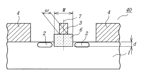
Fig. 5 is a cross sectional view showing an example of the first
optical waveguide modulator according to the present invention. Hereupon,
the similar parts in the following figures to ones in Figs. 1 to 3 are
depicted by
the same numeral.
An optical waveguide modulator 40, shown in Fig. 5, has the
substrate 1 made of a material with an electrooptic effect, the optical
waveguide
2 to guide a lightwave, the travelling wave-type signal electrode 3 and the
ground electrodes 4. And a buffer layer 6, embedded in the supe~cial layer of
the substrate 1 is formed only under the electrode 3 and its nearby part,
having a
width "W" larger than the width "cn" of the electrode 3.
The position of the travelling wave-type signal electrode on the
buffer layer is not limited if the buffer layer is so located that both sides
are
beyond the both sides of the electrode. From the reasons for applying the
electrical field of microwave symmetrically to each optical waveguide and
keeping the chirp of the modulator to be zero, etc., the travelling wave-type
signal electrode 3 is preferably formed symmetrically to the center axis 7 of
the
buffer layer 6.
In the present invention, for lowering the driving voltage of the
modulator, the width of the travelling wave-type signal electrode is
preferably
determined so as to enhance the interaction between the microwave travelling
in
the signal electrode and the lightwave guiding in the optical waveguide.
Concretely, the optical waveguide modulator 40, shown in Fig. 5 preferably has
-9-
CA 02305279 2000-04-07
99812 (PCT/JP99/04321)
a "W/c~" ratio of 1.3 to 6, more preferably 1.5 to 3, which is a ratio of the
width
"W" of the buffer layer 6 to the width "c~" of signal electrode 3.
The width "~" of the travelling wave-type signal electrode 3, as
shown in Fig. 5, as above-mentioned, is the width of the face of the signal
electrode 3 contacting the buffer layer 6.
The width "W" of the buffer layer 6 is preferably 6.5-42 ~.m, more
preferably 7.5-21 ~m since the width "cn" of the travelling wave-type signal
electrode 3 is usually set to be S-7 ~tm, according to the width of the
optical
waveguide, its designed characteristic impedance and an effective refractive
index of a microwave as the electrical signal.
The embedding depth of the buffer layer into the superficial layer of
the substrate is not restricted if the driving voltage can be reduced by
employing
the configuration of the optical waveguide modulator according to the present
invention . However, in the case of the optical waveguide modulator 40, the
embedded depth "d" in the superficial layer of the substrate 1 is preferably
5-10 ~.m, more preferably 6-8 Vim. Thereby, the driving voltage of the
modulator can be further lowered and the effective refractive index of the
microwave can be reduced. The reduction of the effective refractive index
improves the velocity matching between the lightwave and microwave to be
capable of broadening the modulation bandwidth of the optical waveguide
modulator.
Fig. 6 is a cross sectional view showing a variant example of the
optical waveguide modulator shown in Fig. 5. An optical waveguide
modulator 50, shown in Fig. 6, has a buffer layer 8 in which the center part
of
the buffer layer 8 having a width "p" is embedded in the superficial layer of
the
substrate 1, which is different from the modulator 40, shown in Fig. 5.
In such a case of embedding the part of the buffer layer into the
superficial layer of the substrate, the effective refractive index of the
microwave
- 10-
CA 02305279 2000-04-07
99812 (PCT/JP99/04321 )
travelling in signal electrode and the electrical characteristic impedance in
the
whole optical modulator can be adjusted. Thereby, the modulator is optimized
according to the desired operation bandwidth thereof and the excess loss of
the
lightwave guiding in the optical waveguide can be lowered.
Fig. 7 is a cross sectional view showing a variant example of the
optical waveguide modulator shown in Fig. 6.
An optical waveguide modulator 60 shown in Fig. 7 has ground
electrodes 4 embedded in the superficial layer of the substrate 1. Such a
modulator having the ground electrodes of which at least a part of them is
embedded in the superficial layer of the substrate enables the driving voltage
of
the optical waveguide modulator to be extremely lowered.
The embedded depth of the ground electrode in the superficial layer
of the substrate is not particularly limited, but in the optical waveguide
modulator 60 shown in Fig. 7, the embedded depth "D" is preferably 5-10 p.m,
more preferably 6-8 ~.m. For even reduction of the driving voltage in the
branched right-and-left optical waveguides 2, the right-and-left ground
electrodes preferably have the same embedded depth "D".
Figs. 8 and 9 are cross sectional views showing other examples of the
optical waveguide modulator according to the present invention.
An optical waveguide modulator 70, shown in Fig. 8, has a
passivating film 9 on the main surface 6a of the buffer layer 6 on which the
travelling wave-type signal electrode 3 is formed. On the other hand,
an optical waveguide modulator 80 shown in Fig. 9, has a passivating film 10
on
the side face 6b of the buffer layer 6 besides the main surface 6a.
The formation of the passivating film, at least on the main surface of
buffer layer on which the travelling wave signal electrode is formed enables
the
propagation loss of microwave due to the moisture absorbed into the buffer
layer,
to be reduced.
-11-
CA 02305279 2000-04-07
99812 (PCT/JP99104321 )
The material applicable for the passivating films 9 and 10 is not
restricted if it can prevent the absorption of the moisture into the buffer
layer.
However, the passivating film is preferably made of at least one of a nitride
such
as SiN or Si-O-N and a silicon because a dense film of them is easily
obtained.
The buffer layer in the present invention may be made of a well
known material, such as silicon dioxide or alumina.
The travelling wave-type signal electrode and ground electrode may
be made of a well known metallic material such as Au, Ag, or Cu, having a high
conductivity and capable of being easily plated.
The substrate in the present invention is not limited if it is made of a
material having an electrooptic effect. A material such as lithium niobate,
lithium tantalite (LiTa03) or lead lanthanum zirconate titanate (PLZT) may be
used. When the substrate is made of such a material, its main surface may be
composed of every kind of cut face such as an X-cut face, Y-cut face, or Z-cut
face in the material.
In the case of making the substrate of the material such as lithium
niobate, in view of lowering propagation loss of lightwave and preventing the
degradation of the electrooptic effect, the optical waveguide is preferably
formed by doping elements such as Ti, Ni, Cu or Cr, into the substrate through
a
thermal diffusion method.
A fabrication process of the optical waveguide modulator according
to the present invention will be described hereinafter, with reference to the
drawings.
First of all, a photoresist for fabricating an optical waveguide pattern
is spin-coated in a tluckness of 0.5 ~m on the substrate 1, made of lithium
niobate, etc., and thereafter is exposed and developed to form an optical
waveguide pattern having a width of 6-8 Vim.
Then, a layer made of an optical waveguide-forming substance such
- 12-
CA 02305279 2000-04-07
99812 (PCT/JP99/04321)
as Ti is deposited in a thickness of about 800 on the optical waveguide
pattern
by a vacuum evaporation method, and a strip pattern of the deposited substance
is formed employing a lift-off technique. Thereafter, the substrate 1 with the
strip pattern is thermally treated at 950-1050°C for 10-20 hours to
diffuse the
substance into the substrate 1 and form an optical waveguide having a width of
8-11 ~.m.
Subsequently, a concave portion having a depth equal to the depth
"d" to embed the buffer layer is formed in the superficial layer of the
substrate 1
by dry-etching technique with electron cyclotron resonance (ECR) equipment
through a Cr-mask. Thereafter, the Cr-mask is chemically removed, and a
layer made of material such as silicon dioxide is formed, by sputtering, in a
thickness of about 0.5-1.5 p.m so as to embed the concave portion.
Then, as above-mentioned, the buffer layer 6 having the width "W"
is formed by dry-etching tlu-ough a Cr-mask.
Herein, in the case of embedding the ground electrodes 4 into the
superficial layer of the substrate, concave portions having depths equal to
the
depth "D" to embed the ground electrodes is formed in the superficial layer of
the substrate by the above dry-etching.
Subsequently, an underlayer made of a metallic material, such as Ti
or nichrome, is deposited, by a vacuum evaporation method, in a thickness of
about 0.05 p.m entirely on substrate 1, and thereafter an electrode material
layer,
such as Au etc., is deposited, by a vacuum evaporation method, in a thickness
of
0.2 ~m on the underlayer.
Then, a photoresist is spin-coated in a thickness of about 25 ~.m on
the electrode material layer, and thereafter is exposed and developed to form
an
electrode pattern. Next, the travelling wave-type signal electrode 3 having
the
width "cn" of 5 ~.m and ground electrode 4 are formed by electro-plating
having
a thickness of 15-20 Vim.
-13-
CA 02305279 2000-04-07
99812 (PCT/JP99/04321 )
Then, the remaining photoresist is removed with an organic solvent
such as acetone, and thereafter the parts of the underlayer and the electrode
material layer exposed between the travelling wave-type signal electrode 3 and
the ground electrodes 4 are chemically etched and removed using by applicable
etchant, such as aqueous solution of iodine and potassium iodide for Au.
Herein, not shown in Fig. 5, a complete chip for optical waveguide
modulator is mounted on a case made of stainless steel and electrical
connectors
bonded to the travelling wave-type signal electrode 3 and the ground
electrodes
4. Finally, optical fibers are connected to the input and output ends of the
optical waveguide 2.
Figs. 10(a) and 10(b) are cross sectional views showing another
example of the optical waveguide modulator according to the present invention.
Figs. 10a and l Ob show an optical modulation part and an attenuator part,
respectively, corresponding to Figs. 3a and 3b.
The configuration of the conventional optical waveguide modulator
30, shown in Figs. 2 and 3, is different from that of the modulator 90, shown
in
Figs. 10(a) and 10(b), in regards to with or without buffer layer in the
attenuator
part 29. Thus, the optical waveguide modulator 90 will be explained
hereinafter with reference to Figs. 2 and 10.
In the case that the optical waveguide modulator has the attenuator
part according to the present invention, the thickness of the buffer layer in
the
attenuator part is required to be thinner than that in the optical modulation
part.
Moreover, the attenuator part 29 preferably has no buffer layer as shown in
Fig. 10(b). Thereby, the driving voltage of the attenuator part is more
reduced
and the DC drift, due to the buffers layer is almost prevented.
In the case of forming the buffer layer in the attenuator part,
proportion of it's thickness is preferably set to be not more than 0.5, more
preferably to be not more than 0.3, when the thickness proportion of the
buffer
- 14-
CA 02305279 2000-04-07
99812 (PCT/JP99/04321 )
layer in the optical modulation part is set to be 1.
A buffer layer 24 and signal electrodes 15, 17 in the optical
waveguide modulator 90, shown in Figs. 2 and 10, may be made of the same
materials as those in the modulator 40 shown in Fig. 5.
The optical waveguide modulator 90 shown in Figs. 2 and 10 may be
produced by fundamentally same process of the modulator 40 shown in Fig. 5.
However, after the layer made of silicon dioxide, etc. is formed, only the
part of
the layer positioned in the attenuator part 29 is removed by dry-etching
technique. Thus, the fabrication process of the modulator 90 is different from
that of the modulator 40 in regard to the forming process of the buffer layer.
The optical waveguide modulator 90, shown in Figs. 2 and 10
according to the present invention will be modulated as follows:
The lightwave having a wavelength ~1, is incident into the
waveguide 90, passing through metal-cladding type waveguide polarizer 23, and
is on/off-switched by an effect of interference in the optical modulation part
28
as following manners.
A first Y-branch of the first Mach-Zehnder interferometer 12 splits
the propagating lightwave into two equal beams. Their phases are
electrooptically shifted in opposite direction during their propagation along
the
first Mach-Zehnder arms, and the phase-shifted beams are recombined in a
second Y-branch of the first Mach-Zehnder interferometer 12.
If an electric field applied from the signal electrode 15 produces a
phase shift of 7z radians between the two beams, they are cancelled due to
interference. This condition represents a "off-state" of an optical signal in
the
communication system.
On the contrary, if the phase shift is zero or 2~ radians, intensity of
the recombined beams recovers to a level before splitting in the first Y-
branch.
In tlvs condition, the optical signal is in a "on-state".
-15-
CA 02305279 2000-04-07
99812 (PCT/JP99/04321 )
In the case of "on-state", the lightwave having the wavelength ~,1
propagates into the attenuator part 29. Operation in the attenuator part 29 is
basically same as that of the optical modulation part 28. An intensity of the
propagating lightwave is attenuated by choosing appropriate operation point
between the "on" and "ofP' states of the second interferometer 13. In tlvs
manner, the intensity of the propagating lightwave is adjusted to an optimum
level in the communication system.
The intensity-adjusted lightwave passes through metal-cladding type
waveguide polarizer 24 and is detected as an optical signal of a communication
system. The communication system consists of multiple optical waveguide
modulators, as above-mentioned, corresponding to lightwaves having different
wavelengths and thereby intensity of every optical signal in the communication
system is maintained to be constant.
According to the present invention, both of optical modulation part
28 and attenuator part 29, in the optical waveguide modulator 90 shown in
Figs. 2 and 10, modulate the intensity of the lightwave, as above-mentioned.
Since the lightwave is modulated by the effect of interference, the optical
waveguides in optical modulation part 28 and the attenuation part 29 has to be
branched type.
In Figs. 2 and 10, as a preferred embodiment of such a branched type
optical waveguide, are exemplified the first and second Mach-Zehnder type
interferometers 12 and 13. Instead of Mach-Zehnder interferometer, a
directional coupler may be an alternative to the optical waveguide
constituting
the attenuator part 29.
Herein, the optical waveguide modulator 90 shown in Figs. 2 and 10,
has the metal-cladding type waveguide polarizers 23 and 24 at both its input
and
output sides of waveguide. However, the optical waveguide modulator,
according to the present invention, does not always require a polarizer. Thus,
a
- 16-
CA 02305279 2000-04-07
99812 (PCT/JP99/04321 )
polarizes may be provided only in the input or the output in the optical
waveguide modulator. Even though no polarizes is provided, the object of the
present invention is sufficiently achieved.
Examples:
This invention is concretely described on the examples, with
reference to the drawings.
(Example 1)
In this example, the optical waveguide modulator 40 shown in Fig. 5,
was fabricated.
The substrate 1 was made of an X-cut face of a lithium niobate.
Then, a photoresist was spin-coated in a thickness of 0.5 ~.m on the main
surface
of the substrate l, and was exposed and developed to form an optical waveguide
pattern having a developed width of 7 ~.m.
Then, a layer made of Ti was deposited, by a vacuum evaporation
method, in a thickness of 800I~ on the optical waveguide pattern and was
thermally treated, in an electrical furnace, at 1000°C for 10 hours to
diffuse Ti
into the substrate 1 and form the optical waveguide 2, having a width of 9
p.m.
Subsequently, the concave portion having the depth "d" of 7 p.m was
formed in the superficial layer of the substrate 1 by an ECR dry-etching
through
a Cr-mask. Thereafter, a layer made of a silicon dioxide material was formed,
by a sputtering method, in a thickness of 1 pm on the substrate 1 so as to
cover
the concave portion.
Then, after a Cr-mask was formed on the silicon dioxide-layer, the
buffer layer 6 was patterned in the width "W" of 13 ~m by ECR dry-etching.
After removing the Cr-mask, an underlayer made of Ti was deposited,
by a vacuum evaporation method, in a thickness of 0.05 p.m entirely on the
substrate l, and thereafter an evaporated layer made of Au was formed, in a
thickness of 0.02 ~.m by a sputtering method.
-17-
CA 02305279 2000-04-07
99812 (PCT/JP99/04321 )
Then, after a photoresist was spin-coated in a thickness of 25 ~m on
the Au evaporated layer, it was exposed and developed to form an electrode
pattern. Then, an electro-plating was performed with the electrode pattern to
form an Au plated layer having a thickness of 15 Vim. The Ti underlayer and
Au layer were chemically etched to form the travelling wave-type signal
electrode 3 having the width "cn" of 5 ~m and the ground electrodes 4.
The complete chip 1 was mounted on a case made of a stainless steel
(not shown) and optical fibers were connected to the input and output ends of
the optical waveguides 2 (not shown).
The driving voltage of the fabricated optical modulator was 3.4V
And the characteristic impedance and the effective refractive index of
microwave of the optical modulator were 55 S2 and 2.4, respectively.
The microwave-propagation loss of the fabricated optical modulator
scarcely degraded, nevertheless the modulator was exposed to the atmosphere
for several days.
(Example 2)
In this example, the optical waveguide modulator 60, shown in Fig. 7,
was fabricated.
The modulator was fabricated in almost same process though
concave portions for embedding ground electrodes were additionally formed to
have the depth "D" as 7 Vim, employing an ECR dry-etching through a Cr-mask.
The driving voltage of the fabricated modulator was 3.0V
The characteristic impedance and the effective refractive index at microwave
of
the modulator were 51 S2 and 2.4, respectively.
The microwave-propagation loss of the fabricated optical modulator
scarcely degraded, nevertheless the modulator was exposed to the atmosphere
for several days.
(Comparative Example 1)
-18-
CA 02305279 2000-04-07
99812 (PCT/JP99/04321 )
Except for buffer layer 5, formed over the entire main surface la of
the substrate l, and without the removal of the buffer layer 6 by dry-etching,
the
optical waveguide modulator 10, shown in Fig. 1, was fabricated exactly as in
the above examples.
The driving voltage of the modulator was 4.0V and the characteristic
impedance and the effective refractive index of microwave were 54 S2 and 2.4,
respectively.
The propagation loss of the microwave in modulator was measured
with time as above-mentioned. The result of measurement showed that
electrical 3dB-bandwidth was degraded from 10 GHz to 8 GHz after exposing
the modulator in the atmosphere. That is, this optical modulator turned out to
be degraded with time.
As is apparent from Examples l, 2 and Comparative Example l, the
optical waveguide modulator according to the present invention can reduce its
driving voltage though the modulator of the present invention has the same
characteristic impedance and effective refractive index of microwave as those
in
the conventional modulator. And it is also shown that the modulator
configuration of present invention successfully prevent its degradation with
time
derived from the increase of the propagation loss of microwave, because it is
effective to prevent the moisture-absorption of the buffer layer.
(Example 3)
In this example, the optical waveguide modulator 90, shown in
Figs. 2 and 10, was fabricated by the above-mentioned process.
The substrate 11 was composed of an X-cut face of a lithium niobate.
The first and second interferometers 12 and 13 were formed by thermal
diffusion of Ti. The first signal electrode 15 and the first ground electrodes
16;
the second signal electrode 17 and the second ground electrode 18 were formed
by vacuum evaporation and thereafter plating of Au. The electrode length "L"
-19-
CA 02305279 2000-04-07
99812 (PCT/JP99/04321 )
of the first signal electrode 15 and the electrode length "1" of the second
signal
electrode 17 were 4 cm and 2 cm, respectively. The buffer layer 24, in the
optical modulation part 28, made of silicon dioxide, was formed in a thickness
of 1.1 ~.m.
The driving voltage of the fabricated optical waveguide modulator 90
was measured by applying a voltage to the second signal electrode 17, of the
attenuator part 29, in the modulator 90. As a result, its half wavelength
voltage
"Vn" was S.1V
The drift of the DC bias voltage with time, what is called as the DC
drift, in the optical waveguide modulator 90 was measured by carrying out a
high temperature-electric screening test at 80°C. The obtained results
were
shown in Fig. 11.
As is apparent from Fig. 11, the optical waveguide modulator
according to the present invention does not exhibit the drift of its bias
voltage
with time, showing that the DC drift of the modulator has suppressed enough.
(Comparative Example 2)
In this comparative example, the optical waveguide modulator 30
shown in Figs. 2 and 3 was fabricated by similar process as one in Example 3.
However, the buffer layer 14 made of a silicon dioxide was formed uniformly in
a thickness of 1.1 ~.m on the substrate 11, which is different process from
the
Example 3.
The driving voltage of the fabricated optical waveguide modulator 30
was measured by applying a voltage from the external electric power supply to
the second signal electrode 17 of the attenuator part 29 in the modulator 30.
As a result, its half-wavelength voltage "Vn" was 11.4V As is apparent from
Fig. 12, the DC drift voltage in the conventional optical waveguide modulator,
is
increased with time.
As is apparent from Example 3 and Comparative Example 2, the
- 20 -
CA 02305279 2000-04-07
99812 (PCT/JP99/04321 )
optical waveguide modulator, according to the present invention, can reduce
its
driving voltage in its attenuator part and prevent its DC drift.
As is explained above, the first optical waveguide modulator
according to the present invention can reduce its driving voltage and enhance
the
modulation efficiency without increase of propagation loss of microwave and
degradation of velocity matching.
Moreover, the second optical waveguide modulator having the
attenuator part according to the present invention, can reduce the driving
voltage
of the attenuator part without damaging the function of the buffer layer
preventing the lightwave-absorption of the electrodes.
(Industrial Applicability)
The first optical waveguide modulator may be used preferably for a
waveguided optical intensity-modulators, a phase-modulators, a polarization
scramblers, or the like in a high speed and large capacity-optical fiber
communication system. Moreover, the second optical waveguide modulator
having the attenuator according to the present invention may be used
preferably
for a WDM system.
-21-