Note: Descriptions are shown in the official language in which they were submitted.
CA 02305317 2000-03-28
06-10-1999 - 1 - DE 009802912
GR 97 P 2716 P
PCT/DE98/02912
Description
Micromechanical sensor and method for operating the
sensor
The invention relates to a micromechanical
sensor according to the preamble of claim 1 and to a
method for operating a micromechanical sensor according
to claim 9.
A micromechanical sensor of this type is
disclosed in the form of a micromechanical silicon
pressure sensor in DE-C 44 18 207 C1, for example,
which sensors essentially comprise a diaphragm which is
clamped on all sides and bulges when there is a
pressure difference between the two diaphragm surfaces.
The signal conversion is performed for example using
integrated monocrystalline or dielectrically isolated
polycrystalline piezoresistors or by means of
capacitance measurements with respect to a fixed
counterelectrode (piezoresistive or capacitive signal
conversion). A customary requirement made of such
sensors is that their properties ought not to change
appreciably over the course of time. Particularly in
the case of sensors relevant to safety, such as for
example in active occupant protection devices in the
motor vehicle sector (airbag), it is desirable that
specific changes to be noticed, in particular defects,
be identified immediately and, in response, measures be
taken to preclude inadvertent faulty reactions. A self-
test that can be carried out directly for pressure
sensors is not known at the present time. In indirect
self-tests, it is possible to distinguish between
passive and active self-tests. An active self-test can
be performed by means of a defined electrostatic
deflection and corresponding sampling of the resulting
sensor signal. In this case, however, significant
AMENDED SHEET
CA 02305317 2000-03-28
06-10-1999 - la - DE 009802912
GR 97 P 2716 P
PCT/DE.98/02912
difficulties exist: firstly a counterelectrode is
required for the electrostatic deflection of a silicon
pressure sensor
CA 02305317 2000-03-28
06-10-1999 - 2 - DE 009802912
GR 97 P 2716 P
PCT/DE98/02912
diaphragm, such a counterelectrode not being present in
silicon pressure sensors fabricated by means of bulk
micromachining. In pressure sensors fabricated by means
surface micromachining (or more generally in the case
of capacitively sampled pressure sensors), although
there is a suitable counterelectrode, typically very
high deflection voltages are nonetheless necessary (at
least a few 10 V for a pressure range around
approximately 1 bar), which are not available, however,
on sensor modules having a typical operating voltage of
approximately 5 V. A passive self-test of a pressure
sensor with just one diaphragm can usually be effected
only if the sensor is exposed to a precisely defined or
known reference pressure. However, this is not normally
the case, with the result that neither changes in the
accuracy nor possible damage to the sensor can be
identified by means of a passive self-test.
EP-A-0 753 728 discloses a differential
semiconductor pressure sensor having two measuring
diaphragms operating in opposite phases, which enables
the static pressure error and temperature error to be
eliminated by the detection of the different
deflections of the two measuring diaphragms.
US-A-5 022 270 has disclosed a transmitter with
a pressure sensor and an additional pressure sensor,
the additional pressure sensor being used to increase
the measurement range or for redundancy purposes.
US-A-5 431 057 has disclosed a pressure sensor
with a multiplicity of individual sensors arranged on a
matrix, the individual sensors being connected via
connecting arms in order to increase the capacitance
and thus obtain a higher output signal.
The invention is based on the object of
developing a micromechanical sensor, in particular a
pressure sensor, with
AMENDED SHEET
CA 02305317 2000-03-28
06-10-1999 - 3 - DE 009802912
GR 97 P 2716 P
PCT/D~98/02912
self-testing which can be fabricated in a technically
simple manner. Furthermore, the sensor is intended to
be suitable for applications relevant to safety in the
motor vehicle sector and to enable self-testing which
is sufficiently reliable but can be implemented in a
simple manner. A further object consists in specifying
a method for operating the sensor.
This object is achieved, on the one hand, by
means of a micromechanical sensor having the features
of claim 1 and, on the other hand, by means of a method
for operating a sensor having the features of claim 8.
Advantageous developments of the invention
emerge from subclaims 2 to 5.
The invention provides for the active element
to comprise at least two partial structures which are
exposed to the same physical quantity to be measured,
for each partial structure to supply a measurement
signal to the evaluation circuit, and for the
evaluation circuit to have a comparison circuit in
which the at least two measurement signals are compared
and which supplies a comparison signal as a result. An
essential idea of the invention is that the active
element of the sensor, that is to say the pickup, in
particular capacitive pickup, which normally supplies
the useful signal, comprises at least two partial
structures whose supplied information items are
averaged. Partial damage can then be identified by
virtue of the fact that the signals of the two partial
structures are compared with one another. If both
partial structures are in order, the resultant
comparison signal should produce a predetermined value,
e.g. ideally zero in the case of a differential signal;
with tolerance-dictated differences being taken into
consideration, or on account of possible offset
corrections, a test signal is produced which at most
AMENDED SHEET
CA 02305317 2000-03-28
06-10-1999 - 3a - DE 009802912
GR 97 P 2716 P
PCT/DE98/02912
deviates slightly from the predetermined "zero value"
but depends hardly at all on the physical input
quantity (for example the pressure) to be measured. In
the case of partial damage to the sensor, a signal is
produced which deviates distinctly from the "zero
value" and, in comparison with the desired signal of
the undamaged sensor, enables damage to be identified.
Following the principle of the invention, the
at least two partial structures of the active element
are designed to be functionally or constructionally
identical. By 'virtue of the identical construction
and/or identical circuitry of the partial structures,
it is ensured that the signals supplied by the partial
structures of the active element are practically
identical.
In the case of a particularly preferred
development of the sensor, outputs of the two partial
structures are coupled to inputs of a sigma-delta
converter.
AMENDED SHEET
CA 02305317 2000-03-28
GR 97 P 2716 - 4 -
- Foreign version -
In the case of the invention's method for
operating the sensor, in order to generate a useful
signal (from which the measured value is determined),
the partial structures are driven in such a way that
their output signals are added, and, in order to
generate a diagnostic signal (which is used to
ascertain whether the sensor is in order), the partial
structures are driven in such a way that their output
signals are subtracted.
Further advantages and advantageous
developments and embodiments emerge from the exemplary
embodiments which are described below in connection
with Figures 1 to 5. Specifically, in the
illustrations:
Figure 1 shows a schematic cross section through a
capacitive pressure sensor;
Figure 2 shows a schematic plan view of the pressure
sensor;
Figures 3 and 4 show a schematic illustration of the
operation of the pressure sensor;
Figure 5 shows a schematic block diagram of further
circuitry of the pressure sensor with
alternately in-antiphase or in-phase driving.
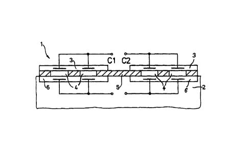
The capacitive pressure sensor 1 in Figures 1
and 2 is a micromechanical sensor. The latter has at
least two diaphragms 3 made of a thin, doped
polysilicon film, which are produced on a silicon
substrate 2 by means of micromechanical methods and
straddle the cavities 4 in an oxide layer 5 that are
formed on the surface of the silicon substrate 2, and
bulge when the pressure to be measured takes effect.
The diaphragms 3 act as first electrodes of the
capacitors C1 and C2; a respective well region 6 doped
into the silicon substrate 2 serves as the second
electrode or counterelectrode,
CA 02305317 2000-03-28
GR 97 P 2716 - 5 -
- Foreign version -
the cavities 4 being situated above said well region.
The monolithic pressure sensor 1 is thus
fabricated by means of surface-micromechanical methods
("surface micromachining"), where, in addition to
polysilicon, another suitable electrically conductive
material can also be used for the diaphragm material,
in order to capacitively sense the diaphragm
deflections.
A significant advantage of this pressure sensor
over a pressure sensor fabricated by means of so-called
bulk micromachining, in which the diaphragms are
produced from monocrystalline silicon and
piezoresistive signal acquisition is used, is that
process steps similar to those used in the fabrication
of conventional integrated circuits are used and,
accordingly, the required circuits (not shown in
Figures 1 and 2) for the signal processing can be
produced using the CMOS process steps with the aim of
simpler integration.
The plan view according to Figure 2 shows two
identically constructed partial structures 7 and 8
(with overall capacitors C1 and C2) each comprising (by
way of example) six square individual diaphragms. The
number and shaping of the individual diaphragms are
inherently arbitrary; it is advantageous if the two
partial structures 7 and 8 are each constructed
identically and interconnected to form the overall
capacitors C1 and C2, as is illustrated schematically
in the cross-sectional view according to Figure 1. The
identical construction of the partial structures and
the circuitry ensure that their capacitances C1 and C2
are practically identical. The absolute value of C1
and/or C2 is typically approximately 2 pF; a pressure
signal of 100 Pa produces a change in the capacitance
of typically 0.15 fF. Incidentally, this imposes
stringent requirements on the eval,~ation electronics.
CA 02305317 2000-03-28
GR 97 P 2716 - 6 -
- Foreign version -
In the block diagrams of the circuitry of the
pressure sensor 1 in accordance with Figures 3 and 4,
for the sake of simplicity the partial structures of
the sensor are represented by the capacitors C1 and C2
and the evaluation circuit, which is likewise formed in
an integrated manner from the silicon substrate 2 of
the sensor component, is provided with the reference
numeral 9.
In accordance with Figure 3, the capacitors C1
and C2 are driven in-phase by the signals 13, 14, the
outputs of the capacitors C1 and C2 jointly being
connected to the clocked switch 12 connected upstream
of the circuit arrangement 9. The circuit arrangement 9
and the switch 12 schematically represents an analog
to-digital (A/D) converter which, in turn, has a
second-order sigma-delta modulator and a two-stage
digital decimation filter (not specifically illustrated
in the figures).
This driving results in a useful signal which
is provided essentially by the sum of the two
individual signals of C1 and C2. For entirely
satisfactory sensors the following holds true: C1 is
identical to C2 and C1 + C2 produce a pressure
dependent useful signal.
In accordance with Figure 4, the capacitors C1
and C2 are driven in-antiphase by the signals 15, 16.
This driving results in subtraction of the capacitive
input signals and a diagnostic signal which is provided
by the difference between the two individual signals of
C1 and C2 and is used to ascertain whether the sensor
is in order.
The diagnostic signal is ZERO (apart from a
possible offset correction) in the case of entirely
satisfactory sensors and has a value other than ZERO if
CA 02305317 2000-03-28
GR 97 P 2716 - 7 -
- Foreign version -
The principle of the invention is not
restricted, however, to the circuitry example,
demonstrated in Figures 3 and 4, with either strictly
in-phase or strictly in-antiphase driving of the
individual capacitors C1 and C2. Rather, more complex
circuitry arrangements are also possible.
In this regard, Figure 5 illustrates a further
exemplary embodiment, in which the (alternately driven)
capacitors C1 and C2 are respectively assigned to
separate switches 17, 18, which are in turn assigned to
two separate inputs of an evaluation circuit 11
designed as an operational amplifier circuit or
comparator circuit.
CA 02305317 2000-03-28
GR 97 P 2716 - 8 -
- Foreign Version -
List of reference symbols
1 Capacitive pressure sensor
2 Silicon substrate
3 Polysilicon film
4 Cavities
5 Oxide layer
6 Well region
7, 8 Partial structures
9, 11 Evaluation circuits
12 Clocked switch
13, 15, 16 Signals
14,
17, Clocked switch
18