Note: Descriptions are shown in the official language in which they were submitted.
CA 02305368 2000-03-30
WO 99/18727 PCTIUS98/21069
DIGITAL VIDEO SYSTEM AND
METHODS FOR PROVIDING SAME
Background of the Invention
1. Field of the Invention
The present invention relates generally to portable video player technology
and the
processing of video images and, more particularly, to techniques for
deinterlacing and enhancing
video images.
2. Description of the Related Art
1o There has been a rapid evolution from analog video technology to digital
video
technology because of the advantages that digital video has to offer. Digital
video can be stored
and distributed more cheaply than analog video because digital video can be
stored on randomly
accessible media such as magnetic disc drives (hard disks) and optical disc
media known as
compact discs (CDs). Once stored on a randomly accessible media, digital video
may become
interactive, allowing it to be used in games, catalogs, training, education,
and other applications.
One of the newest products to be based on digital video technology is the
digital video
disc, sometimes called "digital versatile disc" or simply "DVD." These discs
are the size of an
audio CD, yet hold up to 17 billion bytes of data, 26 times the data on an
audio CD. DVD
storage capacity (17 Gbyte) is much higher than CD-ROM (600 Mbyte) and a DVD
can deliver
2o the data at a higher rate than CD-ROM. Therefore, DVD technology represents
a tremendous
improvement in video and audio quality over traditional systems such as
televisions, VCRs and
CD-ROM.
However, a major problem in utilizing DVD and other digital video technology
to display
motion pictures is that is that the sources of motion pictures come at
different frame speeds. For
example, standard film is shot at a rate of 24 Hz while a television broadcast
using the National
Television System Committee (NTSC) standard updates motion at 60 Hz.
Converting the
motion picture into digital video through a process called deinterlacing often
produces a
noticeable reduction in resolution as well as distortions known as motion
artifacts.
1
CA 02305368 2000-03-30
WO 99118727 PCT/US98/21069
Another problem with utilizing digital video technology is that motion
pictures come in
various formats. For example, movies in the theater are formatted for a wide
screen while video
displays are often much narrower. Video image scaling converts a digital or
digitized image
from one format to another. For example, a digital image with a spatial
resolution of 720
horizontal by 480 vertical pixels may have to be converted to another
resolution in order to be
displayed on a particular display device such as a LCD panel with a fixed
resolution of 640 x
480. However, most prior art video scaling methods provide poor resolution in
the converted
image. The scaling methods that provide quality resolution are extremely
expensive to
implement.
to Yet another problem with video image scaling is that it may require the
transfer of data
between two asynchronous and/or different data rate domains. Using the example
in the above
paragraph, scaling from 720 horizontal pixels to 640 pixels (9:8 ratio)
requires an interface
between a 54 Mhz domain and a 48 Mhz domain (9:8 ratio). In the prior art, the
transferring of
data between two asynchronous and/or different data rate domains used large,
expensive buffers.
Another reason that digital video technology has been difficult to utilize is
because DVD
players are typically large, cumbersome devices that are difficult to
transport. Because DVD
players must be operationally attached to a video display, such as a
television or television
monitor, they are virtually impossible to use anywhere space is limited.
Furthermore, prior art
mobile video systems suffer from a large number of annoying problems. Hand-
held and mobile
television sets typically exhibit reception maladies such as RF rnultipath
interference and poor or
erratic signal strength in rural areas. Integrated TVIVCR combo units can
counter these problems
by providing tape playback capability, but they tend to be physically large
and not truly portable.
In view of the foregoing, it is desirable to have a portable video player
capable of being
easily transported and being used under a wide variety of conditions. It is
further desirable to
have a method and apparatus of deinterlacing and reformatting that provides
for preservation of
the full resolution of an image, while at the same time eliminating motion
artifacts. It is further
desirable to have a method and apparatus for providing high quality video
scaling and vertical
processing while minimizing cost. It is desirable to have a method and
apparatus that provides
for an asynchronous data interface while minimizing cost and eliminating the
need for large and
3o expensive buffers.
2
CA 02305368 2005-02-08
Summary of the Invention
It should be appreciated that the present invention can be implemented in
numerous ways, including as a process, an apparatus, a system, a device or a
method.
Several inventive embodiments of the present invention are described below.
Accordingly, in one aspect of the present invention there is provided a
digital
image enhancer comprising:
a video processor receptive to an interlaced video stream and providing a
deinterlaced video stream comprising:
a first deinterlacer operative to analyze progressive frames of said
interlaced video stream in an attempt to determine an original source type and
sequencing used for the interlaced video stream and further operative to
convert said
interlaced video stream into a deinterlaced video stream using a conversion
process
that is dependent upon detection of said original source type and sequencing;
and
a second deinterlacer operative to reduce motion artifacts detected by a
frequency analysis of said interlaced video stream; and
an output processor receptive to said deinterlaced video stream and operative
to provide a scaled, deinterlaced video stream.
According to another aspect of the present invention there is provided a
digital
image enhancer comprising:
a deinterlacing processor receptive to an interlaced video stream and
operative
to provide a deinterlaced video stream; and
a video output processor receptive to the output of said deinterlacing
processor, wherein said deinterlacing processor processes said interlaced
video stream
in vertical slices to provide a scaled, deinterlaced video stream.
According to yet another aspect of the present invention there is provided a
digital image enhancer comprising:
a deinterlacing processor receptive to an interlaced video stream and
operative
to provide a deinterlaced video stream and operative to analyze progressive
frames of
said interlaced video stream in an attempt to determine an original source
type and
sequencing used for the interlaced video stream; and
3
CA 02305368 2005-02-08
sequencing used for the interlaced video stream; and
a video output processor receptive to the output of said deinterlacing
processor, wherein said deinterlacing processor processes said interlaced
video stream
in vertical slices to provide a scaled, deinterlaced video stream.
In yet another aspect of the present invention, a portable DVD player is
disclosed. The portable DVD player includes a generally thin prismatic
enclosure
having a first major surface, a second major surface separated from said first
major
surface, and side surfaces connecting the first major surface to the second
major
surface. At least a portion of the first major surface includes a video
display, and the
enclosure includes a DVD entry port such that a DVD can be inserted into the
enclosure.
The portable DVD player also includes a digital processing system including a
decoder, an image enhancement engine, and a display controller. The decoder
receives signals from a DVD inserted into the enclosure to provide a decoded,
interlaced video signal. The image enhancement engine converts the interlaced
video
signal to a deinterlaced video signal. The display controller uses the
deinterlaced
video signal to provide progressively scanned video on said video display.
According to still yet another aspect of the present invention there is
provided
a method for processing digital video comprising:
deinterlacing an interlaced video stream with a video processor by at least
one
of a number of deinterlacing methods to produce a deinterlaced video stream,
said
video processor having a first deinterlacer and a second deinterlacer, said
deinterlacing methods including at least one of an original source detection
method, a
diagonal feature detection method, and a motion artifact detection method; and
scaling said deinterlaced video stream.
Other aspects and advantages of the invention will become apparent from the
following detailed description, taken in conjunction with the accompanying
drawings,
illustrating by way of example the principles of the invention.
4
CA 02305368 2000-03-30
WO 99II8727 PCT/US98/21069
Brief Description of the Drawings
The present invention will be readily understood by the following detailed
description in
conjunction with the accompanying drawings. To facilitate this description,
like reference
numerals designate like structural elements.
Figures lA and 1B illustrate a portable DVD player in accordance with one
embodiment
of the present invention.
Figures 2A, 2B, and 2C illustrate several different applications for the DVD
player in
accordance with one embodiment of the present invention.
Figure 2D illustrates a docking station and associated video monitor for the
DVD player
1o in accordance with one embodiment of the present invention.
Figure 2E illustrates a "DeskTabletTM" DVD player in accordance with one
embodiment
of the present invention.
Figure 3 is a block diagram of the electronic circuitry of the DVD player in
accordance
with one embodiment of the present invention.
Figure 4 illustrates a system diagram of the Image Enhancement Engine (IEZ) in
accordance with one embodiment of the present invention.
Figure 5 illustrates a method of combining fields into frames in a
deinterlacing process in
accordance with one embodiment of the present invention.
Figure 6 is a block diagram of a video deinterlacer in accordance with one
embodiment of
the present invention.
Figure 7 is a system diagram of a progressive frame detector in accordance
with one
embodiment of the present invention.
Figure 8 is a flow diagram of the processing steps within a field-differencing
module in
accordance with one embodiment of the present invention.
Figure 9 illustrates details of the frequency detection module in accordance
with one
embodiment of the present invention.
5
CA 02305368 2000-03-30
WO 99118727 PCT/US98/21069
Figure 10 is a system diagram of the PFPD module in accordance with one
embodiment
of the present invention.
Figure 11 is an illustration of a deinterlace process in accordance with one
embodiment
of the present invention.
Figure 12 shows a two-dimensional array of pixel values used to describe the
present
invention.
Figure 13 is a diagram illustrating a method for using obtaining an output
pixel from the
two-dimensional array of Figure 12 in accordance with one embodiment of the
present invention.
Figure 14A is an illustration used to describe the method in accordance with
one
1o embodiment of the present invention.
Figure 14B is a graph of a set of samples from the sampling line of Figure
14A.
Figure 14C is a graph of a sampled cosine wave.
Figure 15 is an illustration used to describe the method of thresholding a
detection value
in accordance with one embodiment of the present invention.
Figure 16 is a block diagram of a mixing circuit in accordance with one
embodiment of
the present invention.
Figure 17 is a diagram of an exemplary operation of the mixing circuit in
accordance with
one embodiment of the present invention when the DV is greater than "0," but
less than "1."
Figure 18 is an illustration of a method for detecting diagonal features in
accordance with
one embodiment of the present invention.
Figure 19 is a block diagram of a diagonal mixing circuit in accordance with
one
embodiment of the present invention.
Figure 20 is a diagram showing the pixels of secondary array used for
calculating the
output of the diagonal mixing circuit of Figure 16.
Figure 21 is a flow chart of a diagonal detection method in accordance with
one
embodiment of the present invention.
6
CA 02305368 2000-03-30
WO 99/18727 PCTNS98/21069
Figure 22 is an example of a variable scaling FIR filter in accordance with
one
embodiment of the present invention.
Figure 23 is a graph of low-pass filter coefficients in the time domain.
Figure 24 is a table of coefficients organized into L sets of mutts per set.
Figure 25 is a flow chart of a method for quantization in accordance with one
embodiment of the present invention.
Figure 26 is a flow chart of a method for changing coefficients in accordance
with one
embodiment of the present invention.
Figure 27 illustrates a video frame in accordance with one embodiment of the
present
1o invention which is subdivided into a number of vertical slices for a slice
scanning sequence
exemplified by a corresponding number of scan lines.
Figure 28 illustrates an example of an initial slice core that has a problem
with
unavailable data on its left edge and right edge.
Figure 29 illustrates a slice that has added wings along the initial slice
core's left and
right edges.
Figure 30 illustrates an overall structure of overlapping slice/wing
combinations.
Figure 31 is a flow chart illustrating a method of processing video in
accordance with one
embodiment of the present invention.
Figure 32 illustrates a system diagram for a slice based video processor in
accordance
2o with one embodiment of the present invention.
Figure 33 illustrates a system diagram of a video processing chip architecture
in
accordance with one embodiment of the present invention.
Figure 34 is a diagram of an asynchronous interface in accordance with one
embodiment
of the present invention.
Figure 35 is a diagram of an alternative asynchronous interface in accordance
with one
embodiment of the present invention.
7
CA 02305368 2000-03-30
WO 99118727 PCT/US98/21069
Figure 36 is a diagram of a 3-buffer synchronizer sequence illustrating the
sequencing
and relative relationships of read and write operations to three RAM buffers
in accordance with
one embodiment of the present invention.
Figure 37 is a flow chart of a method for sequencing through RAM addresses and
modules in accordance with one embodiment of the present invention.
Figure 38 is a diagram of a synchronizer of the present invention configured
for use in a
video scaling application in accordance with one embodiment of the present
invention.
8
CA 02305368 2000-03-30
WO 99!18727 PCT/US981Z1069
Detailed Description of the Preferred Embodiments
In the following description, numerous specific details are set forth in order
to provide a
thorough understanding of the present invention. It will be understood,
however, to one skilled
in the art, that the present invention may be practiced without some or all of
these specific
details. In other instances, well known process operations have not been
described in detail in
order not to unnecessarily obscure the present invention.
Figures lA and 1B illustrate a portable DVD player 10 in accordance with one
embodiment of the present invention. The DVD player 10 includes a housing 12
that serves as
an enclosure or chassis for the components of the DVD player 10. A screen 14
for viewing the
1 o video and control buttons 16 to control the DVD player 10 are located on
the top face of the
housing 12. Power and signal interfaces 18 are located on one of the two side
faces of the
housing 12, while an infrared (IR) interface 20 and a media transport 22 are
located on the other
side face. A DVD 24 can fit within a suitably configured recess in the media
transport 22, and
the media transport 22 withdraws into the housing 12 to permit the playback of
DVD 24.
Figure 2A shows an illustration of use in an automobile, but the idea can be
extended to
most types of transportation. The present invention is ideally suited to the
traveler who spends
long hours in a passive commute, such as on an airplane, train, or subway as
illustrated in Figure
2B. In addition, many commercial applications are possible as well, for
example, video
advertising in taxicabs or other settings where a captive audience exists. The
present invention
2o can also be placed on the magazine rack of every Stairmaster~ exercise
machine and treadmill in
a fitness center setting, as illustrated in Fig. 2C.
Wherever portable video playback is needed, the present invention can be
there.
Anywhere great sound, DVD and CD playback, or TV viewing is desired, the
present invention
will be the ideal mobile solution. Great examples of the versatility of the
present invention uses
are: air travel entertainment, movies, videos, personal education and study
(each disc is capable
of storing thousands of books), and on-the-spot do-it-yourself videos in
topics such as auto
repair, gardening, cooking, home proj ects.
Furthermore, the present invention can be used as a portable video display
device for
video games, camcorder playback, or digital still camera image viewing, and
for OEM
3o applications such as video kiosks, commercial airliners and fitness
centers. The portable DVD
9
CA 02305368 2000-03-30
WO 99118727 PCTIUS98/21069
player 10 can also be used to present sales content: bus, elevator, taxicab,
real estate walk
through videos, etc. It can even be utilized as a hang-it-on-the-wall flat
television or display
device - fine art discs, "dynamic art", etc.
Figure 2D illustrates a "Home Theater Docking Station" provides an
uncomplicated, one-
s step connection and operation capability for when the present invention is
used as a simple DVD
player with a normal home television set. The dock provides a cabled
electrical interface to a
television or other home theater components - such as an audio system - that
can remain
permanently in place for when the present invention is used with an external
system. The dock is
preferably the same form-factor as a typical VCR; it will be designed to blend
in with the rest of
1o the system components that a user owns, and also be instantly recognizable
for its intended
function.
An infrared remote control is preferably bundled with the docking station. The
remote
features a comprehensive control feature set optimized to access all of the
additional enhanced
features available with the DVD format. Central to the design of this remote
control is a highly
15 attractive industrial design that will carefully avoid the dreaded and
difficult-to-use "sea of
buttons" so commonly found on consumer product remotes.
Figure 2E illustrates one embodiment in accordance with one embodiment of the
present
invention for the desktop market is referred to herein as a "DeskTabletTM" DVD
player.
Applications for the DeskTablet include uses such as in the bedroom, den, or
kitchen, where a
20 "fixed" unit placement is needed. This product is essentially in the same
marketing space as
conventional TV/VCR combination units. Similar in form factor to the
"Monorail" personal
computer, the thin DeskTablet form factor will be capable of either
freestanding or wall hanging
operation. Freed of many of the portability-driven design constraints required
of the present
invention mobile machine, the DeskTablet will include a high-quality
integrated loudspeaker
25 system.
Figure 3 is a block diagram of the drive module 26 of the DVD player 10 of
Figures 1
and 2. The drive module 26 includes the media transport 22 that reads the DVD.
Video data
from the DVD is then transferred over to a MPEG/Doiby digital (or "MPEG/AC-3")
decoder 28.
After decoding, an Image Enhancement EngineTM (IEZ) 30 deinterlaces the
digital video to
3o provide a progressively scanned video signal. Finally, the video is
displayed through a display
36.
CA 02305368 2000-03-30
WO 99/18727 PCT/US981210b9
The DVD drive module 26 also includes an audio/infrared link 32, a system
controller 34,
a battery pack 38, a power supply 40, a video data buffer 42, and a user
interface, among other
illustrated components, busses, and sub-systems. The components of the DVD
drive module 26
are primarily housed within the housing 12 and will each be described in
detail below.
The DVD transport 22 preferably uses an off the-shelf drive module 26 designed
for
portable computers. Preferably, the drive module 26 is seventeen mm or less in
thickness,
allowing a very thin system form factor. A suitable DVD drive module 26 is
available from
Toshiba America Information Systems, Inc. of Tokyo, Japan. Further, the drive
module 26 of
the present invention is preferably physically and electronically isolated
from mechanical shocks
to and impacts. More particularly, the drive module 26 is mechanically shock
mounted in the
housing 12, and data from the drive module 26 is buffered in memory for a
period of time before
decoding to allow sectors to be reread in the event of a shock-induced data
stream discontinuity.
The MPEG/Dolby digital decoder 28 is preferably an off the-shelf single-chip
decoder
targeted at consumer DVD players. It preferably performs both MPEG-1 and MPEG-
2
decoding, Dolby digital ("AC-3"), MPEG, and LPCM audio decoding, has A/V
synchronization,
and has the characteristic that only a single memory device is required for
data storage and
buffering. Such decoders are available from a variety of sources, including C-
Cube
Microsystems of Milpitas, California.
The IEz 30 preferably deinterlaces digital video from DVD or any other source
to provide
progressively scanned video signal, including proprietary motion detection and
compensation
hardware. It further preferably corrects brightness, contrast, gamma, and
color temperature
correction for clear and accurate video display. To further improve the image,
a high quality
scaling engine of the IEZ 30 is preferably used to convert video image from
rectangular to square
pixels and to scale the video for full-screen display on flat panel sizes
other than 640 x 480.
The audio/IR link 32 (comprising one or more integrated circuit chips) decodes
the Dolby
digital data stream provided from MPEG2/Dolby digital decoder 28, mixes 5.1
channels down to
2 channels for conventional stereo output, and encodes/processes 5.1 channels
for surround
headphone output (optional module). Stereo D/A converters are provided for
headphone output.
D/A converters for 5.1 channel Dolby digital stream are available on the
docking module
3o connector. An undecoded Dolby digital stream for outboard decoders is also
available on the
11
CA 02305368 2000-03-30
WO 99/18727 PCT/US98I21069
docking module connector. An optional IR transmitter for wireless headphones
may be
provided, as may stereo speakers with small stereo power amp for presentations
or playback
without headphones.
The system controller 34 is preferably a single-chip microprocessor handling
most, if not
all, system control functions. For example, the microprocessor preferably
handles system startup
and configuration, user interface & controls, feature set selection (e.g.,
parental control, etc.),
DVD drive control, and IEz, MPEG decoder, audio system, and display controller
configuration.
A suitable microprocessor is available as part number MC68HC16 from Motorola,
Inc. of
Austin, Texas.
to The display 36 is preferably an 11.3" LCD display (both active and passive
matrix
models available) with high-output fluorescent cold cathode backlight. The
display 36
preferably has 640 x 480 pixel resolution and 18-bit color depth. A suitable
display is available
from Sharp Electronics Corp. of Camas, Washington. The video controller for
the display 36
provides high-resolution, flexible onscreen graphics, overlay of graphics onto
full-screen video
playback, and LCD drivers for direct connection to display.
The housing 12 is preferably made with a "tablet" form factor, which is easy
to use and
carry. The single piece housing design of the enclosure provides simplicity,
ease of manufacture,
ruggedness, reduced weight, and serviceability. An optional docking station
allows simple one-
connection hookup to external video systems.
2o The battery pack 38 is preferably a replaceable, rechargeable module based
upon NiMH
technology for high power density at low cost. Preferably the battery pack
uses standard, off
the-shelf battery cells having a 40 watt-hour capacity which provides
sufficient power for over
2.5 hours of continuous operation. This period of time is normally sufficient
to view a full,
feature-length movie.
Also shown are inputs and outputs to/from the unit. While interconnections
from the
system controller 34 to other components are shown as a bus, these may in fact
be realized via
discrete connections if appropriate for the specific off the-shelf components
chosen. The
architecture of the DVD drive module 26 has been designed for modularity of
components and
ease of expandability.
12
CA 02305368 2000-03-30
WO 99/18727 PCTIUS98/21069
System expansion is accomplished via an I/O option module interface, which
allows the
drive module 26 to interact with the video and audio subsystems, as well as
the system controller
34. This interface accommodates expansion modules with functions such as
alternate audio
and/or video inputs and specialized audio processing, allowing the present
invention to be
customized by the user for a variety of applications.
Alternate product configurations are easily accommodated by substitution of
key system
components. Since standard components are used in many areas of the system
(e.g., the DVD
drive module 26), similar components can simply be substituted. For instance,
a more compact
unit can be built by utilizing a smaller LCD and battery. The display
controller directly
1o accommodates varying display sizes, while the power converter and battery
charger are
configurable for different battery sizes and technologies. More fully
functioned base
configurations are possible by simply including additional (optional)
components for added
functionality. For example, a unit with a full complement of video and audio
I/O requires only
the addition of extra D/A converters, a video decoder, extra connectors, and
enclosure
modifications.
The system software of the portable DVD player of the present invention is
preferably
structured into two main levels: the high-level user interface software and
the low-level device
control software. The software runs on the system microcontroller 34, and is
preferably stored
on a read only memory ("ROM") (not shown). The low-level section interfaces
directly with the
2o various hardware components of the system, interacting directly with them
at a register level. It
provides for power-on and initialization, configuration of the hardware
components, basic device
control and synchronization, and interface to the user interface software.
Between the two levels the present invention provides a "control/status"
Application
Program Interface ("API"). This is a moderately high level interface, with the
API functions
corresponding almost directly with the typical user controls - e.g., "play,"
"skip to next track,"
"show elapsed time," etc. The control functions provide a means for the user
interface software
to issue commands for control of the player, while the status functions allow
the user interface
software to acquire information about the state of the player hardware.
This architecture permits customized user interface software. The
"control/status" API
3o provides a clean break between the user interface and the low-level device
control software,
allowing another user interface, e.g., a customized user interface, to be
substituted into the
13
CA 02305368 2000-03-30
WO 99/18727 PCTIUS98/21069
player's standard software. It will therefore be appreciated that the software
architecture of the
present invention can support a variety of product configurations, allowing a
rich product family
with excellent longevity and scalability.
A power supply 40 includes a DC-to-DC power converter to allow the use of an
internal
battery or external DC source. The DVD player 10 preferably derives all
required internal
voltages from a single DC power source. A high voitage inverter provides power
needed for
display back light. A charger (not shown) is used to re-charge the internal
rechargeable battery.
The user interface includes a straightforward control strip on the front bezel
for quick access to
common functions, and the software user-interface allows full-featured, yet
simple and intuitive
to player control. Software controls rendered via high-resolution graphics can
overlay video for
immediate user feedback.
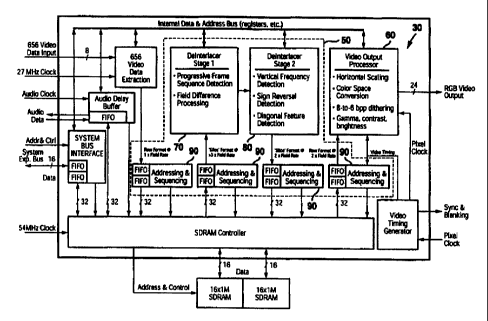
Figure 4 illustrates a system diagram of the Image Enhancement Engine (IEZ) 30
(see
Figure 3) in accordance with one embodiment of the present invention. The IEZ
30 includes a
two dimensional video processing chip architecture 50 and a video output
processor 60. The
~5 chip architecture 50 includes a first deinterlacing stage 70 and a second
deinterlacing stage 80
and a set of addressing and sequencing FIFOs 90. The first deinterlacing stage
70 includes
progressive frame sequence detection and field difference processing. The
second deinterlacing
stage 80 includes vertical frequency detection, sign reversal detection and
diagonal feature
detection. The video output processor 60 includes horizontal scaling, color
space conversion, 8
2o to 6 bpp dithering and gamma, contrast, and brightness corrections.
The first deinterlacing stage 70 of Figure 4 is discussed in greater detail
with reference to
Figures 5-10. Figure 5 illustrates a method 100 of combining fields into
frames in a
deinterlacing process in accordance with one embodiment of the present
invention. A series of
film frames 102 at 24 frames per second are converted to video fields 104 at
60 fields per second.
25 The video fields 104 are then converted to deinterlaced frames 106 by a
deinterlacing process.
The deinterlaced frames 106a are created by combining the two most recent
fields into a single
frame, but the deinterlaced frames 106b are created by combination of
different video fields and
distinguished by bold arrows and bold borders.
Refernng to Figure S, when Field 2 is the "current" field, then DI Frarne 1 is
created by
3o combining Field 1 {the "last" field) and Field 2 (the "current" field). DI
Frame 2 is created in the
same way by combining Field 3 with Field 2 when Field 3 is the current field.
In contrast, when
14
CA 02305368 2000-03-30
WO 99118727 PCT/US98/21069
Field 4 is the current field, combining Field 4 and Field 5 creates DI Frame
_3. In this case, the
combination is the "current" and the "next" fields. When the field combination
is done in this
way, all of the deinterlaced fi-ames 106 will be created by combining fields
that originate from
the same source frame. Because these combining fields originate from the same
source frame,
they are time correlated. Therefore, no motion artifacts exist in the
deinterlaced frames 106.
Combining fields into frames as shown in Figure 5 requires identification of
the type of
motion picture used in the original source. First, a source must be identified
to be one in which
original progressive frames exist; second, the sequencing used to create
fields from the frames of
the original source must be determined in order to assemble video fields into
frames and avoid
to artifacts.
Figure 6 is a block diagram of a video deinterlacer 130 in accordance with one
embodiment of the present invention. A digital video stream enters the
deinterlacer 130 through
a FIFO memory module 132 before being written into a digital memory unit 134.
The digital
memory unit 134 has the capacity to store four complete video fields in a set
of field buffers
134a-d. The incoming field is written to each of the field buffers 134a-d in
sequence. Therefore,
the first incoming video field is written to field buffer 134a, the second
incoming video field is
written to field buffer 134b, etc. After field buffer 134d is filled, the next
incoming video field is
written to field buffer 134a again.
During the time period of one field, the incoming field is written to one
field buffer 134,
2o and the three previous fields are read from the other field buffers 134.
For example, if as shown
in Figure 6, the incoming field is written to 134a, then field buffers 134b-d
are being read into a
set of FIFO memories 136, 138, and 140. The FIFO memories 136, 138 and 140 are
provided to
accommodate the reading and writing of the four video fields into a single
physical memory unit
134, and also to decouple the clocking domains of the incoming video, the
memory unit 134, and
the subsequent deinterlace processing stages.
The labeling of the field buffers in 134a-d as "incoming," "1st," 2nd," and
"3rd" previous
fields are from the point of view of the incoming video streams. The outputs
of the three read
FIFOs 136, 138, and 140 are labeled Next Field, Current Field, and Last Field
respectively. This
labeling is from the point of view of the deinterlace processor 130 and
implies that deinterlace
3o processing imposes a delay of approximately two field time periods on the
video stream.
CA 02305368 2000-03-30
WO 99/18727 PCT/US98I21069
The oufiputs of FIFOs 136, 138, and 140 are synchronized so that the three
fields
presented to subsequent processing stages are spatially concurrent. The three
fields are then
presented as inputs to an inter-field progressive frame detector 142 which
produces a last/next
(L/l~ signal 144, a progressive frame detection (PFD) signal 146 and a stage 1
detection value
(StagelD~ 148. The L/N signal 144 is a control signal that instructs a field
assembly stage 150
to assemble the Current Field with the Last Field or the Next Field, which are
three sequential
fields from the input video stream.
With the three fields, the field assembly stage 150 produces a progressively
formatted
output frame 152. If the Current Field is even, then the Next and Last Fields
must be odd and
to vice versa. Therefore, the progressively formatted frame 152 output of the
field assembly stage
150 will always be a combination of one even and one odd field. This is
important because the
correct assembly of fields into progressive frames requires one even field and
one odd field for
input.
The optional intra-frame deinterlacer 154 may provide additional processing to
remove
artifacts that occur within the output frame 152 under certain conditions,
such as when the PFD
signal 146 is de-asserted. If the frame detector 142 detects that the incoming
video signals were
originally from a source that contains progressive frames, the PFD signal 146
is asserted. Three
original types of source video are detected: film at 24 frames per second,
computer animations or
frames rendered at 30 frames per second, or still images, in which no motion
occurs in the image
over a period of several fields. When the PFD signal 146 is asserted, the
optional processor 154
is disabled.
However, if the frame detector 142 is unable to detect a progressive frame
sequence from
the incoming video fields, then it will set the LIN signal 144 to always
assemble Current and
Last fields in the field assembly stage 150. Then, the frame detector 142 de-
asserts the PFD
signal 146, which informs the optional deinterlacer 154 that artifacts may be
present in the output
frame 152 and that further processing may be necessary to remove the artifacts
and create a final
progressive output frame 152'.
Detection of a progressive frame sequence requires keeping a history of the
preceding
fields. However, the progressive frame detector 142 can look only one field
ahead. In cases
3o where a large transition in the image occurs, it is possible for the
progressive frame sequence to
change because of edits in the original video source. These changes could
require changes in the
16
CA 02305368 2000-03-30
WO 99/18727 PCT/US98/210G9
way frames are created from incoming fields, but it is not possible to know in
advance of the
arrival of the incoming fields.
For this reason, the progressive frame detector 142 must be capable of
detecting
transitions in the motion picture because transitions may indicate edits that
may change the
progressive field sequencing. If a transition is detected, the progressive
frame detector 142 will
de-assert the PFD signal 146 for the time period required to determine the new
progressive frame
sequence. This allows motion artifacts to be removed by the optional
deinterlacer 154 during the
time period needed to reacquire the progressive frame sequence. In cases where
a progressive
frame sequence is not detected and the PFD output is not asserted, the
StagelDV 148 output
to contains magnitude information related to the amount of motion present in
the image. This
information may be used in the optional deinterlacer 154 to further process
the image.
Figure 7 is a system diagram of a progressive frame detector 142 in accordance
with one
embodiment of the present invention. The frame detector 142 includes a field
differencing
module 154, a frequency detection module 156, and a progressive frame pattern
detection
~5 (PFPD) module 158. The field differencing module 154 calculates the
difference between a Next
Field 160 and a Last Field 162, processes the differences into the StagelDV
148, a transition
detection 3:2 value 166, and a plurality of equal field history bits 168.
The frequency detection module 156 combines a Current Field 164 and the Last
Field
162 into a frame and then detects the vertical high frequencies that result
from motion artifacts.
2o Then, the frequency detection module 156 outputs a number of frequency
detection history bits
170 and a transition detection 2:2 value 172. Finally, the PFPD 158 takes as
input the transition
detection 3:2 value 166, the plurality of equal field history bits 168, the
frequency detection
history bits 170 and the transition detection 2:2 value 172 to produce the L/N
signal 144 and the
PFD signal 146.
25 Figure 8 is a flow diagram of the processing steps within the field-
differencing module
154 in accordance with one embodiment of the present invention. A Next array
of pixels 174,
which is a subset of the Next Field 160, and a Last array of pixels 176, which
is a subset of the
Last Field 162 are the inputs to a differences 178. The Next and Last pixel
arrays 174 and 176
can be viewed as windows moving across their respective fields. The "window"
is moved from
30 left to right and top to bottom. Each time the windows are moved, a new
difference is computed.
The result of the difference operation 178 is an array of differences 180.
17
CA 02305368 2000-03-30
WO 99118727 PCT/US98/21069
Using a weighted average of the array of differences 180, the StagelDV 148 is
computed.
The weighting is such that the difference values near the center of the array
of differences have
the most influence on the weighted average. The array of differences 180 is
also input into a
f eld difference accumulator 182 that sums the differences over the entire
field to produce a field
difference value 184. The previous five field difference values are stored in
a memory module
186 and are summed in an operation 188.
The sum of the previous five field difference values is compared to the
current field
difference value in an operation 190, and the result is the Transition 3:2
output signal 192. The
current field difference value 184 is compared in a threshold operation 194
with the value in a
to programmable field difference register 196. The result of the threshold
operation 194 is an equal
field bit 198, which is a single bit that indicates that the Next Field 160
and Last Field 162 are
the same. The previous equal field history bits 168 are stored in a memory
module 200 and are
used in the PFPD 158 of Figure 7.
Figure 9 illustrates details of the frequency detection module 156 in
accordance with one
embodiment of the present invention. Vertically adjacent pixels 206 from the
Current Field 164
and the Last Field 162 are assembled, as they would appear spatially on a
display. A frequency
detection value is calculated in an operation 208. This calculation is
performed to detect the
frequencies that are associated with deinterlaced motion artifacts. In an
operation 210, the output
of the frequency detection is compared with a programmable threshold value
212. The results of
2o five adjacent frequency detection values are stored in a memory module 214
and are summed in
an operation 216.
The output of the operation 216 is accumulated over the entire field period in
a field
frequency detection accumulator 218 to produce a field frequency detection
value 220. The field
frequency detection value 220 is stored in a memory module 222 that contains
the previous 5
field frequency detection values. The five previous field frequency detection
values are summed
in an operation 224 and the results are compared to the current frequency
detection value 220 in
an operation 226. The result of this comparison in operation 226 is the
Transition 2:2 bit 228,
which indicates that a transition has occurred in the 2:2 sequence.
As part of a parallel process, a first previous field detection value 230 that
was stored in
the memory module 222 is transferred to a multiplier 232, and multiplied with
a value stored in a
programmable field frequency threshold register 234. The result of the
multiplication is
18
CA 02305368 2000-03-30
WO 99118727 PCT/US98/21069
compared in an operation 236 to the current field frequency detection value
220. The result is a
relative frequency difference bit 238, which is then stored in a memory module
240. The
previous ten relative frequency difference bits 242 are output to the PFPD
module 158.
Figure 10 is a system diagram of the PFPD module 158 in accordance with one
embodiment of the present invention. The PFPD module 158 performs logical
operations on a
set of field difference history bits 244, the frequency detection history bits
242, the transition 3:2
value 192 (see Figure 8), and the transition 2:2 value 228 (see Figure 9).
After the input of the
field difference history bits 244, a logical operation 246 determines the 3:2
pulldown detection
bit by looking for patterns in which every fifth field is equal. Then, a
logical operation 248
detects still images by setting the STILL bit when the most recent four field
differences are
zeros. The state of the L/N control signal is set by a logical operation 250.
From the input of the frequency detection history bits 242, a logical
operation 252 detects
a 2:2 pulldown detection bit by searching for alternating patterns of high
frequency and low
frequencies in successive field times and monitoring the frequency detection
history bits 242.
Then, a logical operation 254 determines the L/N control signal for the 2:2
pulldown case. The
PFD signal 146 is determined from the 3:2 pulldown detection bit, the
transition 3:2 value 192,
the 2:2 pulldown bit, and the transition 2:2 value 228.
Three source types of progressive frames are detected. Film converted to video
using 3:2
pulldown is detected by computing the difference between pairs of even fields
or pairs of odd
2o fields and looking for the condition in which every fifth difference is
zero. This condition is
indicated by the 3:2 pulldown signal. Computer generated animations using 2:2
pulldown are
detected using a frequency detection method which looks for the frequencies
associated with
motion artifacts in every second combined frame, indicated by the 2:2 pulldown
signal. Still
images are detected when the field differences are zero for several
consecutive fields, indicated
by the STILL signal.
Progressive frames are simply the logical OR of these three signals as shown
by a logical
OR gate 256. However, transitions must also be taken into account. As
mentioned above, a
transition is a large change in the field sequence that results from edits, or
dropout of the video
signal. If a large change is detected, then progressive frame detection, which
depends on a
3o history of several fields, may be unreliable for the period required to
establish a progressive
19
CA 02305368 2000-03-30
WO 99/18727 PCT/US98I21069
frame pattern. In the examples illustrated, this period is ten field times or
about one-sixth of a
second for 60 Hz fields.
In a set of logical operation 258, a pulse is generated under two conditions.
One is that a
3:2 pulldown sequence is detected and a transition occurs; the second is a 2:2
pulldown sequence
is detected and a transition is detected in the sequence. Either of these
cases triggers a timer 260
which generates a pulse of a ten field duration, since ten fields is the time
period required to
establish a new progressive sequence. During this time, a logical AND gate 262
disables the
PFD bit 146. As mentioned previously, if the PFD bit 146 is not asserted, then
the optional
infra-frame deinterlace processor 154 (illustrated in Figure 6) may remove
motion artifacts
to during the timeout period.
It will therefore be appreciated that the progressive frame detecting process
of the present
invention provides for elimination of edge artifacts in a video image. This is
accomplished by
identifying the type of the original motion picture and using that information
to help combine
video fields in the deinterlacing process. The combination of these techniques
provides a low-
artifact, high-resolution deinterlaced image.
The second deinterlacing stage 80 of Figure 4 is discussed in greater detail
with reference
to Figures 11-21. Figure I1 illustrates a method 300 of deinterlace
processing. A video field
302 containing scan lines 306, and a previous video field 304 containing scan
lines 308 is fed
into a field combination deinterlace processor 310. Each of the video fields
is 720 pixels by 280
pixels. The result is a 720 pixels by 480 pixels combined frame 312 with scan
lines 314 sourced
from video field 302 and scan lines 316 sourced from video field 304.
When this simple deinterlacing of the prior art is performed, and a motion
picture
formatted for an interlace display is converted to a progressive format, a
noticeable "artifact" or
error arises because the image content of vertically adjacent lines is time
shifted by 1/60' second
as noted previously. The error is most visible around the edges of objects
that are in motion.
Figure 12 shows a two-dimensional array of pixel values 318 that is a subset
of the
combined frame 312 of Figure 11 that will be used to describe the present
invention by way of
example. The array of pixels 318 is shown having a width of 5 and a height of
7 pixels. The
array 318 is labeled across the top CO to C4 indicating columns and is labeled
vertically along
3o the left side from the top to bottom RO to R6 indicating rows. The pixels
contained in array 318
CA 02305368 2000-03-30
WO 99/18727 PCT/US98I21069
are used to compute a frequency detection value. In addition, the array 318 is
also used to detect
diagonal features and finally to compute the resulting pixel.
The array 318 is positioned so that a set of even numbered rows 320 contain
pixels from
the most recent or "current" field of the original source, and a set of odd
numbered rows 322
contain pixels from the previous field. The array 318 is then stepped across
the combined frame
312 (see Figure 11 ) from left to right horizontally. Each step causes the
pixels in each of columns
C1, C2, and C3 and C4 to shift to the column to its immediate left. The pixels
in column CO
shift out of the array 318, and a new column of pixels shifts into column C4.
After the array 318 has been stepped across all the horizontal positions of
combined
io frame 312, it is stepped down vertically by two pixels and returned to the
left side of the
combined frame 312. Therefore, even numbered rows 320 contain pixels from the
most recent
field and odd numbered lines 322 contain pixels from the previous field. The
process then
repeats itself as array 318 is then stepped across the combined frame 312
again from left to right
horizontally. At each position in the two-dimensional array, a detection value
(DV) is calculated.
Figure 13 illustrates a method 326 for obtaining an output pixel 338 from the
two-
dimensional array 318. In an operation 328, a frequency detection value is
obtained using the
seven pixels of each column of the two-dimensional array 318. Because there
are five columns,
there are five frequency detection operations performed, producing a set of
detection values fd0,
fdl, fd2, fd3, and fd4. Next, an operation 330 thresholds the set of detection
values fd0-fd4.
2o Then, in an operation 332, the set of detection values fd0-fd4 is combined
in a weighted average
to arrive at an ultimate detection value (UDV) 334.
The weighting factors may be variables. One weighting example is the
following: UDV
_ (fd0 + (2 * fdl) + (8 * fd2) + (2 * fd3) + fd4)/14. The weighting causes
frequency detection
values closest to the center of array 318 to have the greatest influence on
the UDV 334. In this
way, using five horizontally adjacent frequency detection values results in a
low pass filtering
operation providing smoother transitions between areas within the combined
frame 312 where
motion artifacts do and do not exist.
The UDV 334 computed in operation 332 is used to control a mixing operation
336,
which preferably implements the following equation: pixelout = (UDV * (pR2C2 +
pR4C2)/2) +
((1 - UDV) * pR3C2) where pixelout is the new output pixel of the
deinterlacing operation,
21
CA 02305368 2000-03-30
WO 99/18727 PCT/US98/Z1069
pR2C2 is a pixel in the array 318 at location Row 2, Column 2, pR4C2 is a
pixel in the array 318
at location Row 4, Column 2, and pR3C2 is a pixel in the array 318 at location
Row 3, Column
2.
The result of the mixing operation is that the new value of pixel pR3C2 of the
array 318
depends on the UDV 334. If no motion is detected by the calculation of the UDV
334, then the
pixel at pR3C2 will be the unmodified value of the pixel at that position in
the previous field. If
a large UDV 334, i.e., a value of 1 results, then a strong motion artifact has
been detected, and
the value of pR3C2 is computed by averaging the values of pR2C3 and pR4C3 of
the array 318.
The averaged result will not show motion artifacts because it is created from
values of the most
to recent field that are time correlated with the most recent field. Detection
values that are between
0 and 1 will cause the pixel at pR3C2 to be a mix of pR3C2 and the average of
pR2C3 and
pR4C3.
Figure 14A illustrates an image 340 showing operation 328 in greater detail.
The image
340 shows the computation of a single frequency detection value for one column
of array 318.
Image 340 includes a distorted object 342 which is effected by an interlace
motion artifact. The
image is sampled along a line 344, which is shown for exemplary purposes. This
sampling
corresponds to one of the columns in the two-dimensional array 318. In this
example, line 344
passes through an area where artifacts exist, but in general, a sampling of
vertical adjacent pixels
may or may not contain artifacts.
2o Figure 14B is a graph 346 of a set of samples 348 obtained by sampling
along line 344 of
Figure 14A. The set of samples 348 are plotted with the row numbers along the
horizontal axis
and the brightness or intensity of the pixel along the vertical axis. From
graph 346, it is apparent
that the areas where motion artifacts exist, such as the set of samples 348,
will show a
characteristic frequency. This is frequency in space rather than in time and
is most conveniently
expressed as cycles per line rather than cycles per second or Hertz. The
characteristic frequency
is 1 cycle/2 lines or 0.5 cycle/line.
Figure 14C is a graph of a sampled cosine wave 350. The characteristic
frequency
created by the motion artifact is detected by multiplying the set of samples
348 by the sampled
cosine wave 350. The sampled cosine wave 350 has a frequency equal to the
characteristic
3o frequency of the motion artifact. Then, the result is integrated using the
following equation:
22
CA 02305368 2000-03-30
WO 99118727 PCT/US98/21069
R=6
fd = ~ Y(R) cos(2R ~t * 0.5cycle l line)
R=0
where fd is the frequency detection value for one column of array 318, R is a
line index
corresponding to the RO... R6 of array 318 and has the units "line," and Y(R)
is the set of
vertically adjacent samples 348.
The expression cos {2~R * 0.5 cyclelline) simplifies to 1 for R = 0, 2, 4, and
6 and -1 for
R = 1, 3, and 5. If 1 and -1 are substituted for RO... R6, the frequency
detection equation
becomes: fd = (Y6/2 + Y4 + Y2 + YO/2) - (Y5 + Y3 + Y1). Note that Y6 and YO
are divided by
2 because the integration is over the limits 0 to 6. The final fd is the
absolute value: fd =
Abs(fd). The method 326 of Figure 13 is repeated for each column in array 318,
producing the
1o set of frequency detection values 330.
Figure 15 is a graph 352 illustrating thresholding operation 330 in greater
detail. Each fd
is a number in the range 0 to 1. Graph 352 includes a non-thresholded scale
354 from which
values are thresholded to the thresholded scale 356. Thresholding sets all
values above the upper
threshold point 358 to the value of 1. All values below the lower threshold
point 360 are set to a
value of 0. Values between the upper and lower thresholds are expanded to the
range 0 to 1.
Thresholding can be described with the following equation: tdf = (ptfd - LTH)
/ UTH where tdf
is the thresholded frequency detection value, pthfd is the pre-thresholded
frequency detection
value (the output of operation 328), LTH is the lower threshold value and UTH
is the upper
threshold value. If tfd > 1.0, then tfd = 1Ø Otherwise, if tfd < 0 then tfd
= 0.
2o It will therefore be appreciated that the deinterlacing process of the
present invention
provides good vertical resolution without creating edge artifacts in moving
objects in a video
image. This is accomplished by employing two-field interlacing where the image
is relatively
static, and employing one-field line doubling where the image is rapidly
changing. The
combination of these techniques provides a low-artifact, high-resolution
deinterlaced image.
The UDV 334 is preferably used then in a mixing circuit 400 shown in Figure
16. The
mixing circuit 400 computes a new value for the pixel at location R3C2 of
array 318. If no
motion artifacts are detected, then the value of the UDV 334 will be "0" and
the mixing circuit
400 will output the original pixel R3C2. If the value of the UDV 334 is "1,"
then the mixing
23
CA 02305368 2000-03-30
WO 99/18727 PCT/US98/21069
circuit 400 will output the average of the pixels above and below R3C2, so the
output of the
mixing circuit 400 is the average of R2C2 and R4C2.
Figure 17 is a diagram of an exemplary operation of the mixing circuit 400
when the
UDV 334 is greater than "0," but less than "1." The mixing circuit 400 uses
information from
the three-pixel array 402 by blending R3C2, and the average of R2C2 and R4C2
to form a new
output pixel 406 at location R3C2.
Figure 18 is an illustration of a method 408 for detecting diagonal features.
A secondary
array 410 that is a subset of array 318 is input into a diagonal detection
circuit 412 which
operates in parallel to the method 326 of Figure 13. If no diagonal feature is
detected, then the
1o diagonal detection circuit 412 produces no output. However, if a diagonal
feature is detected, the
diagonal detection circuit 412 produces two outputs: a single bit Sign signal
414 and a multiple
bit SlopeFade signal 416. The specific method for calculating the Sign and
SlopeFade signals
414 and 416 is shown in Figure 21 and its corresponding description.
The Sign signal 414 is used to determine which pair of pixels is diagonally
adjacent to
R3C2. The SlopeFade signal 416 is a measurement of the magnitude of a diagonal
feature.
Magnitude is determined by the amount of contrast along the diagonal feature.
High contrast,
such as a diagonal white line across a black background, will result in the
highest values of the
SlopeFade signal 416. A lower contrast results in a lower value for the
SlopeFade signal 416.
Figure 19 is a block diagram of a diagonal mixing circuit 418 in accordance
with one
2o embodiment of the present invention. The diagonal mixing circuit 418
includes a multiplexer
420, a first mixer 422, and a second mixer 424. The multiplexer 420 relies on
the Sign signal
414 to determine which pair of diagonally adjacent pixels are used. After a
pair of diagonally
adjacent pixels is chosen, the first mixer 422 blends the pixel values that
are vertically adjacent
to R3C2 with those that are diagonally adjacent to R3C2. The amount of
blending is determined
by the SlopeFade signal 416, which is proportional to the magnitude of the
diagonal feature that
is detected.
The second mixer 424 is the final mixing stage and is identical to the mixing
circuit 400
shown in Figure 16. The second mixer 424 produces an output that is determined
by input pixel
R3C2 and the output of the first mixer 422. The UDV 334 is the control input
for second mixer
424. In summary, the new pixel value at R3C2 is computed from pixel values
from the
24
CA 02305368 2000-03-30
WO 99/18727 PCTIUS98/21069
secondary array 410. The control signals for determining the final pixel value
are the UDV 334,
the Sign signal 414 and the SlopeFade signal 416.
Figure 20 is a diagram showing the pixels of secondary array 410 used for
calculating the
output of the diagonal mixing circuit 418. If no diagonal features are
detected within the
secondary array 410, then the output of the mixing circuit is determined from
the pixels along a
line 426. If a diagonal feature is detected in diagonal detection circuit 412,
the pixels that are
diagonally adjacent to R3C2 along a line 428 or a line 430 are used to
calculate the output pixel.
The Sign signal 414 is used to determine which line 428 or 430 is used.
Figure 21 is a flow chart of a diagonal detection method 432 in accordance
with one
1o embodiment in accordance with one embodiment of the present invention. The
method 432
shows the flow of logical and mathematical operations used to compute the
SlopeFade signal 416
and the Sign signal 4I4 from the secondary array 410. The corner pixels are
divided into two
horizontal pairs and two vertical pairs by an operation 434. The horizontal
pairs are labeled hv2
and hv4 and the two vertical pairs are labeled w2 and w4. Differences are
computed for each
1 s pair of corner pixel values by subtraction, producing a pair of horizontal
differences and a pair of
vertical differences.
In an operation 436, the two horizontal and vertical differences are summed to
produce a
horizontal and vertical difference vector for the secondary array 410. An
operation 438
computes the absolute value of the horizontal and vertical difference vectors.
A thresholding
20 value is used to adjust the magnitude of the SlopeFade output 416 in an
operation 440. The
output of operation 440 is an unqualified SlopeFade signal (unQualSlopeFade)
that is still
subject to being "zeroed out" by the DiagDetect signal and the SlopeDisQual
signal produced by
parallel operations of the method 432.
The signs of the horizontal and vertical differences from operation 434 are
recorded and
25 stored in an operation 442. The signs indicate whether the operation 434
resulted in positive or
negative numbers. Then, an operation 444 looks for cases where the signs of
the horizontal and
vertical difference operations are in opposition to each other. If such cases
are found, then
SlopeDisQual is set to "1." If the signs of the difference operations are not
in opposition, then
SlopeDisQual is "0."
CA 02305368 2000-03-30
WO 99/18727 PCT/US98121069
In operation 444, the diagonal detector looks for diagonal features that are
relatively
large; in particular, the feature must be larger than the nine-pixel secondary
array 410 used as the
input to the diagonal processor. Image features that are smaller than the
secondary array 410 can
cause the diagonal processing to incorrectly detect a diagonal feature. These
small features can
be detected by observing the signs and setting SlopeDisQual accordingly.
An operation 446 compares the magnitude of the horizontal and vertical vectors
computed in operation 438 to detect a diagonal feature. Then, the DiagDetect
signal is produced
in an operation 446 using the horizontal and vertical vectors. The ratio of
the difference of the
horizontal and vertical vectors and the sum of the horizontal and vertical
vectors is adjusted by a
threshold value, diagDetThresh.
A final SlopeFade output is computed in an operation 448 in which two single
bit inputs
are used to qualify the SIopeFade output. The first bit is a DiagonalDetect
bit and the second bit
is a SlopeDisQual bit. SlopeFade will be zero if DiagDetect is 0 or if
SlopeDisQual is a 1,
otherwise, SIopeFade will take the value of unQualSIopeFade. The SlopeDisQual
signal changes
the SlopeFade signal to zero for cases where the slope of the diagonal feature
cannot be reliably
calculated.
Finally, the Sign signal 414 is computed in an operation 450 using the sign
bits produced
by the sums of the horizontal and vertical vectors performed in operation 436.
The Sign signal
414 is computed using this logical operation to determine the slope of the
diagonal feature.
2o The video output processor 60 of Figure 4 is discussed in greater detail
with reference to
Figures 22-27. Figure 22 shows an example of a variable scaling FIR filter
500. The variable
scaling FIR filter S00 includes a shift register 502 with a series of
registers 504 each of which is
connected to a clock 506. Each register 504 is connected to one of a set of
multipliers 508, 510,
and 512 by one of a series of filter taps 514. Multipliers 508, 510, and 512
accept two inputs to
be multiplied. The first input is an eight-bit data word, and the second input
is a coefficient.
Multipliers 508, S I0, and 512 differ from each other in that they accept
coefficients quantized to
different numbers of bits. Multipliers 508 use the least number of bits per
coefficient and
multipliers S 12 use the most bits per coefficient. Multipliers 508, S 10, and
S I2 are connected to
a coefficient storage unit 516 and an adder 518.
26
CA 02305368 2000-03-30
WO 99/18727 PCT/US98I21069
Eight bits of data are input into the variable scaling FIR filter 500 through
the shi$
register 502. The output of each register 504 is coupled by one of a series of
filter taps S 14 to
one of a set of multipliers 508, 510, and 512 to be multiplied by a
coefficient produced by the
coefficient storage unit 516. A new set of coefficients is entered into the
multipliers 508, 510,
and 512 by the coefficient storage unit 516 on each cycle of clock 506. The
results from each
multiplier 508, 510, and 512 are summed by the adder 518 to produce a filtered
output sample.
Figure 23 is a graph of low-pass filter coefficients 520 in the time domain
stored in the
coefficient storage unit 516 to produce coefficients. The low-pass filter
coefficients 520 are
represented by the equation below.
l0 ( 1 ) ~ c(i) = 2jc~:fc 1/2) * sin~2 fc~c(i -1/2)~ * {0.54 + 0.46 cos~2~(i -
1/2~/taps~~
The unquantized and continuous wave is represented by a curve 522. Filter
coefficients
524 are shown plotted on or near the curve 522. Some coefficients 524 appear
slightly off the
curve due to the error introduced by quantizing each coefficient to a limited
number of bits.
Figure 24 shows the coefficients 524 organized into L=8 sets of mults=6
coefficients per
set. The sum of all the coefficients in each set i where i=1 to L is
represented by the equation
below.
j~mults
(2) s(i}= ~c(L(j-1)+i)
j=1
Figure 25 is a flow chart of a quantization method 526 in accordance with one
embodiment of the present invention. The method 526 initializes with a given
set of parameters
528 needed to compute the coefficients where L is the numerator of the scaling
ratio LIM; mutts
is the number of multipliers used in the FIR filter; and n is the number of
bits to which the
coefficients will be quantized. An operation 530 computes the FIR filter
coefficients using
equation 1. In an operation 532, the coefficients are organized from left to
right and labeled c(1),
c(2), c(3),...c(L * mutts).
In an operation 534, each coefficient is quantized to n number of bits by
rounding. Next,
an operation 536 starts a loop which is executed L times, one time for each
coefficient set, in
which all the coefficients in each set are summed. An operation 538 sums the
coefficients for
27
CA 02305368 2000-03-30
WO 99!18727 PCT/US98/21069
set(i) represented in Figure 24. Then, an operation 540 tests the result of
the summing operation
538 for a 1.0 result. If operation 540 produces a true result, then no further
processing is done.
The loop iterator is incremented in an operation 542, and control passes back
to operation
536. If operation 540 produces a false result, then a Fudge value F is
computed in an operation
544 by subtracting the sum produced in operation 538 from 1Ø Then,
processing proceeds to an
operation 546 in which one of the coefficients of set(i) is changed so that
the sum of all the
coefficients in set(i) =1Ø
Figure 26 is a flow chart of the operation 546 from Figure 25 in much greater
detail. An
operation 548 is a loop set up to step through the coefficients of set(i) in a
particular order. The
l0 order starts with the outermost coefficient of the set(i), and then moves
toward the center of the
set. Operation 548 is executed molts times, because there are molts number of
coefficients per
set. Next, an index k is computed in an operation 550, which is used to
process the coefficients
in the previously stated order.
The coefficients at the left or right edge of the coefficient set must be
handled as a special
case. Therefore, an operation 552 is performed on the index k to determine
whether the
coefficient to be processed is either the first coefficient, c(1), or the last
coefficient, c{L * molts).
If operation 552 determines that the coefficient to be adjusted is the
leftmost one, that is, c(1),
then an operation 554 is performed.
Operation 554 evaluates whether the absolute value of the sum of c(1) and F is
less than
2o or equal to the absolute value of the coefficient to the right of c(1).
This means that c(k+1) _<
c(2). If the result is true, then c(1) can be adjusted by adding F without
creating a discontinuity
or divergence from the zero axis. The coefficient is adjusted in an operation
564, and operation
546 is exited successfully. If the result is false, then operation 560
performs a loop iteration.
If operation S52 determines that the coefficient to be adjusted is the
rightmost one, that is,
c(L * molts), then the method proceeds to an operation 556. Operation 556
evaluates whether
the absolute value of the sum of c(L * molts} and F is less than or equal to
the absolute value of
the coefficient to the left of c(L * molts), that is, c(L * molts - 1 ). If
the result is true, then c(L
molts) can be adjusted by adding F without creating a discontinuity or
divergence from the zero
axis. The coefficient is adjusted in 564, and operation 546 is exited
successfully. If the
operation 556 result is false, then a loop iteration is performed in operation
560.
28
CA 02305368 2000-03-30
WO 99118727 PCT/US98/21069
If operation S52 determines that the coefficient to be adjusted is neither the
leftmost or
rightmost one, then an operation SS8 is performed. Operation 558 evaluates
whether the sum of
c(k) and F is outside the limits of the coefficients on the left and right,
that is c(k - 1) and c(k +
1), by evaluating the equations c(k-1) < c(k) < c(k+1) and c(k-1) > c(k) >
c(k+1). If either of the
equations is true, then the coefficient c(k) is set equal to c(k) + F in
operation S64 and a
discontinuity is not introduced. Therefore, operation S46 is successfully
exited. If either of the
equations is false, then a loop iteration is performed in operation 560.
Operation 560 increments the loop iterator variable so the next coefficient
can be
evaluated. An operation 562 asks whether all the coefficients in the set(i)
have been evaluated.
to If ail the coefficients in set(i) have not been evaluated, then control is
passed to the top of the
operation S48 and the procedure is repeated for the next coefficient. If all
the coefficients in
set(i) have been evaluated, then the coefficient set cannot be quantized to n
bits without
introducing an unacceptable discontinuity into the coefficient set. Therefore,
n is incremented in
an operation 566 and operation 546 is exited. Control is then returned to the
method S26 at
operation 534 (in Figure 25) where the original coefficients are quantized to
the new value of n
and the process is repeated. In the cases where operation 546 is successfully
exited, control is
returned to the method 526 (in Figure 25) at the operation 538 and the next
coefficient set(i) is
evaluated.
The two-dimensional chip architecture 50 and the addressing and sequencing
FIFOs 90 of
2o Figure 4 are discussed in greater detail with reference to Figures 27-33.
Figure 27 illustrates a
video frame 600 in accordance with one embodiment of the present invention
subdivided into a
number of vertical slices 602 for a slice scanning sequence exemplified by a
corresponding
number of scan lines 604. Each slice 602 is scanned in a format similar to
that used in a
conventional raster-scanned sequence, with the scanning sequence proceeding to
the subsequent
slice when the end of a given slice is reached. The advantage of this format
is that the length of
the line memories is reduced by a factor roughly equal to the number of
vertical slices used.
Line memories are still necessary, but they are now much shorter than before,
resulting in a
much reduced on-chip memory requirement. For instance, if the number of slices
were set to 10,
the reduction in on-chip memory would be by an entire order of magnitude.
3o However, difficulties do arise from utilizing this "slice" scan
organization. First, it is
often the case that processing must simultaneously be done in both the
horizontal and vertical
29
CA 02305368 2000-03-30
WO 99/18727 PCT/US98/21069
directions. This results in a problem on the left and right slice boundaries
where horizontal pixel
data outside the slice may not be available. Second, the conventional raster-
scan sequencing has
been changed, resulting in a potential incompatibility with common video
sources and
display/storage devices. Both of these problems will be addressed in the
following discussion as
solved by the present invention.
Figure 28 illustrates an example of a slice core 606 that has a problem with
unavailable
data on its left edge 608 and right edge 610. For purposes of illustration,
unavailable data is
shown only on the left edge in Figure 28. Video processing requires that data
surrounding a
given pixel be available in both the horizontal and vertical directions {in
this case 5x5 matrices
to 612 and 614 centered on the pixel).
Processing matrix 612 resides in the center of the slice core 606, so there is
no problem
with availability of data because it is available in both horizontal and
vertical directions on all
sides of processing matrix 612. The situation at the top edge 618 and bottom
edge 620 of the
slice core 606, where data above the top-most pixel and data below the bottom-
most pixel is not
available, is identical to that with the conventional raster-scanned format.
This can be solved in a
number of ways, such as substituting zero data for the nonexistent upper/lower
pixel data.
Therefore, the top and bottom edges 618 and 620 of the slice core 606 will not
cause problems
with unavailable data.
In contrast, processing matrix 614 is on the left edge 608 of the slice core
606,
2o horizontally adjacent data. Thus, two columns of pixel data 616 are missing
because they are
outside the left edge 608 of the slice core 606. To resolve this situation,
data for these columns
are provided from the slice immediately to the left of the slice being
processed.
Figure 29 illustrates a slice 622 that includes a pair of thin vertical slices
or "wings" 624
and 626 along the left and right edges 608 and 610. Wing 624 has been added to
the slice core
606 to provide the pixel data needed for the processing matrix. Wing 626 has
been added to the
right edge 610 of the slice core 606. Because wing 624 has been added to slice
622, processing
matrix 614 no longer suffers from the lack of data outside of the left edge
608 of slice 622.
Figure 30 illustrates an overall structure of overlapping slice/wing
combinations 628.
Slice 622 from Figure 29 is shown as an exemplary slice. Wings 624 and 626 of
slice 622 are
3o composed of data from a pair of adjacent slices, one to the left and one to
the right of slice 622.
CA 02305368 2000-03-30
WO 99/18727 PCTIUS98I21069
More specifically, the missing two left columns of pixels in wing 624 are
supplied from the two
right most columns 630 of a slice 632 immediately to the left of slice 622. So
in a sequence of
slices 634, the left-most wing of slice N overlaps the core of slice N-1,
while the right-most wing
of slice N-1 overlaps the core of slice N.
Figure 31 is a flow chart illustrating a method 636 of processing video in
accordance with
one embodiment of the present invention. The input to a video processing block
is therefore the
slice 622 with slice core 606, left wing 624 and right wing 626. The left wing
624 is divided into
a left outer wing 638 and a left inner wing 640. The right wing 626 is divided
into a right outer
wing 644 and a right inner wing 642. In this example, the video processing
block has multiple
to processing stages, each with its own requirement for horizontal pixels on
each side of the center.
The method 636 utilizes a first processing stage 646 and a second processing
stage 650.
The first processing stage 646 utilizes and then removes the outer wings 638
and 644 leaving an
output slice 648 consisting of the slice core 606 and the inner wings 640 and
642. The second
processing stage 650 utilizes and then removes the inner wings 640 and 642.
Therefore, the
wings 624 and 626 are effectively removed in the processing and the output of
the processing
block is a slice 652 with the width equal to the original slice core 606.
One effect of the wings 624 and 626, is to increase the on-chip slice-line
memory
requirements by the width of the wings 624 and 626. However, the wing width is
typically small
relative to the overall slice width. The actual slice and wing width is
implementation dependent
2o and will depend on processing requirements and available external memory
bandwidth.
A preferred embodiment of the present invention utilizes three vertical video
processing
blocks. The first processing stage 646 requires a pair of outer wings 638 and
644 having a width
of 2 pixels; the second processing stage 650 requires a pair of inner wings
640 and 642 with a
width of 4 pixels; and the third processing stage 652 requires no wings as the
specific processing
algorithm used does not require data horizontal to the vertical data being
processed. The slice
core width chosen was 36 pixels, resulting in an initial input slice width of
48 pixels. (Core +
left-inner-wing + right-inner-wing + left-outer-wing + right-outer-wing =
36+4+4+2+2 = 48.)
Unfortunately, the data inputs and outputs of the vertical processing blocks
are not in the
raster-scan video format, which is standard to virtually all video input
sources and video output
3o display and storage devices. The present invention includes a standardized
inputloutput format
31
CA 02305368 2000-03-30
WO 99/18727 PCT/US98/Z1069
conversion, which is accomplished via the use of a memary external to the
video processing
device. A commodity DRAM memory device is used for reasons of cost and
availability.
Depending on the type of video processing to be done, a field or frame size
buffers)
serves other necessary purposes in addition to conversion between full
field/frame raster-scan
and slice-scan formats. For instance, the deinterlacing process typically
requires one (sometimes
several) field buffers to store multiple fields of video data for temporal
processing. Buffers are
also needed in frame rate conversion, where the output frame rate is different
than the input rate;
in this case multiple output field or frame buffers may be required for the
frame rate conversion
process.
io Figure 32 illustrates an example of a system diagram for a slice-based
video processor
654. A first input buffer 656, a second input buffer 658, a first output
buffer 660, and a second
output buffer 662 are required for the slice conversion process. Because video
applications
typically require real-time input and output, and because the scanning process
for a conventional
raster-scan and a slice-scan are different, the first input buffer 656 is used
to store the video input
i5 data stream from the input data formatter 664. The second input buffer 658
(filled in the
previous fieldlframe period) is used to provide data to the vertical video
processing section 666
in a slice-scan format.
A similar process is used for output. The second output buffer 662 receives
processed
data in slice-scan format from the vertical video processing section 666,
while the first output
20 buffer 660 (f lled in the previous field/frame period) is used to output
data in the conventional
raster-scan format to the output data formatter 668. The output data stream
may actually provide
data to additional video processing stages that process data in the horizontal
direction only (e.g.
horizontal scaling and color space conversion).
Figure 33 illustrates a system diagram of one example of a video processing
chip
25 architecture 670. The video processing chip architecture 670 includes a
video processor 672 and
an external memory source 674. In this particular video processing
implementation, multiple
input field storage (for temporal processing) is required. Video data is
provided to an input stage
676 in the video processor 672 that adds the redundant wing data directly into
the video data
stream. The data is then written (wings included) in a raster-scan sequence to
a first field
3o memory buffer 678 in the external memory source 674 by the memory
controller 680 which is
located inside the video processor 672.
32
CA 02305368 2000-03-30
WO 99118727 PCT/US98/21069
In subsequent field periods, data is written to a second field memory buffer
682, a third
field memory buffer 684, and a fourth 686 field memory buffer in sequence.
Next, data is read
from the second, third and fourth field memory buffers 682, 684, and 686, all
of which are in the
external memory source 674 and connected in parallel. The field buffers 682,
684, and 686 feed
the vertical video processing section 688 that is located inside the video
processor 672. The data
is processed in the vertical video processing section 688, which removes the
wings.
Data is written from the vertical video processing section 688 in a slice-scan
format back
to a first frame buffer area 690 in the external memory source 674. Data is
read from a second
frame buffer area 692 in the external memory source 674 in a conventional
raster-scan sequence
to for input to a horizontal processing block 694 located in the video
processor 672. The output of
the horizontal processing block 694 is in raster-scan format and is the output
of the video
processor 672.
In one preferred embodiment of the present invention, video input data is
provided as
interlaced fields of data in a 720x240 pixel field format. Each video field is
conceptually broken
into 20 slices having a width 36 pixels, with each slice having left and right
wings of 6 pixels
each (outer wings of 2 pixels each and inner wings of 4 pixels each). The
wings are added at the
appropriate points in the video input data stream, and the resulting data
stream is written in
raster-scan sequence into a first field buffer in an external SDRAM.
Three fields of data are read from the SDRAM simultaneously. The data for
these fields
2o is sourced by second, third, and fourth field buffers and is read in
vertical slices 48 pixels wide
(slice core and wings) by 240 rows. The data is processed by a first vertical
processing stage that
provides slice-scan format data at twice the input rate of a single field to a
second stage. Slice
data input to the second stage is formatted in slices of 44 pixels wide by 480
rows (due to the
rate-doubling action of the first stage). The second vertical processing stage
processes the data
and provides 36 pixel wide slice-scan format data at the same rate as the
input to that stage to a
third vertical processing stage.
The third stage is a vertical scaler and performs no horizontal processing,
and so does not
require wings on the slice format data. Data is output from the third
processing stage in a 36
pixel wide slice-scan fonmat to a first frame buffer area in the SDRAM. The
number of rows in
3o each slice is dependent on the specific vertical scaling ratio chosen. Data
is input to a horizontal-
only processing stage in conventional raster scan format of 720 x 480*M
pixels, where M is the
33
CA 02305368 2000-03-30
WO 99118727 PCT/US98/21069
vertical scaling factor in the third vertical processing stage. This data is
processed by the
horizontal processor (which includes a horizontal sealer) and is output in a
conventional raster-
scan format at a resolution of 720*N x 480*N, where N is the horizontal
scaling factor.
Overall, this implementation results in a greater than lOX reduction in on-
chip memory
requirements due to the slice-scan architecture. This expense saved with the
reduction in on-chip
memory requirements more than offsets the additional required external memory,
and provides a
variety of prototyping and production options.
The video output processor 60 of Figure 4 is discussed in greater detail with
reference to
Figures 34-38. Figure 34 is a diagram of an asynchronous interface 700 in
accordance with one
io embodiment of the present invention. A data source 702 provides data
synchronous to clock C1
in an input data stream 704 to a synchronizer 705. Once the data has been
received by the
synchronizer 705, a write control logic (WCL) unit 706 directs the writing of
this data into one of
a first RAM buffer 708, a second RAM buffer 710, and a third RAM buffer 712 by
providing
control and address signals to each of the RAM buffers 708, 710, and 712.
Once data has been written into the RAM buffers 708, 710, and 712, a read
control logic
(RCL) unit 714 directs the reading of data from the RAM buffers 708, 710, and
7I2 by providing
address and control signals to the RAM buffers 708, 710, and 712. The
retrieved data is then
output from the synchronizer 705 in a continuous output data stream 716 at
clock rate C2 to a
data destination 718.
2o Reading of data from a given RAM buffer 708, 710, or 712 does not start
until that
particular RAM buffer 708, 710, or 712 has been filled by the WCL unit 706.
After one of the
RAM buffers 708, 710, or 712 has been filled, the next RAM buffer 708, 710, or
712 is written
to in sequence, and data can be read from the previously filled RAM buffers)
708, 710, and/or
712. Although this particular embodiment uses three RAM buffers it should be
understood that
more RAM buffers may be used depending on the system requirements.
A synchronization logic unit 720 external to the synchronizer 705 coordinates
the reading
and writing of data. Optionally, the synchronization logic 720 could be part
of the synchronizer
705 itself. Multiple synchronization schemes may be implemented. For example,
the
synchronization logic 720 could signal the WCL unit 706 and the data source
702 when to start a
3o data transfer. A predetermined period later, when the first RAM buffer 708
has been filled and
34
CA 02305368 2000-03-30
WO 99/18727 PCT/US98/21069
the second RAM buffer 719 is in the process of being filled, the
synchronization logic 720
instructs the RCL unit 714 to begin reading data from the first RAM buffer 708
and to provide it
to the data destination 718.
An alternative scheme could have the data transfer be more or less free
running. The
WCL unit 706 would be accepting data from the data source 702 as it is
available, writing that
data to the next available RAM buffer 708, 710, or 712, and signaling the RCL
unit 714 that the
respective buffer is full. The "buffer full" signal must be synchronized from
the C1 to C2 clock
domain, typically through a dual-rank synchronizer. The RCL unit 714 could
either latch the
state of the "buffer full" signal, or return a handshaking signal (which must
be synchronized
1o from the C2 to C1 clock domains) back to the WCL unit 706 indicating that
either the "buffer
full" signal has been received or that the RAM buffer 708, 710, or 712 has
been emptied.
Figure 35 is a diagram of an alternative asynchronous interface 722. Data
transfer is
initiated via an external signal to the WCL unit 724 that indicates that a
data transfer is to begin.
The WCL 724, synchronous to clock C1, generates write enables and addresses
for the a first
single-ported RAM buffer 726, a second single-ported RAM buffer 728, and a
third single-ported
RAM buffer 730. The single-ported RAM buffers 726, 728, and 730 have
synchronous write
and asynchronous read capabilities.
Only a single write enable is active at any one time, with the write enable
for RAM buffer
726 being asserted first, followed by that for RAM buffer 728, then RAM buffer
730, then back
2o to RAM buffer 726, and so forth. At the point that RAM buffer 728 is full
and RAM buffer 730
is approximately half full, an external signal is asserted to the RCL unit 732
to initiate reading of
the data from the RAM buffers 726, 728, and 730. The RCL unit 732, synchronous
to clock C2,
generates addresses and data select lines far the RAM buffers 726, 728, and
730 for read
operations.
Individual RAM buffers 726, 728, and 730 receive a read or write address based
on
which RAM buffer 726, 728, or 730 is currently being written to, i. e., one
RAM buffer 726, 728,
or 730 being written to receives its address from the WCL unit 724 while the
other two RAM
buffers 726, 728, and 730 receive their addresses from the RCL unit 732. A
data MLTX 734,
controlled by the RCL unit 732, selects the output data stream from the one of
the three RAMs
3o currently being read from. Although in this example, external signals start
the data transfer read
CA 02305368 2000-03-30
WO 99/18727 PCT/US98121069
and write operations, an optional synchronization logic unit 736 may be
present in the absence of
one or more of the external "start" signals.
Figure 36 is a diagram of a 3-buffer synchronizer sequence 738 illustrating
the
sequencing and relative relationships of read and write operations to three
RAM buffers.
Potential clock synchronization delay issues pertaining to real-time buffer
sequencing for the
continuous data output stream are mitigated by the fact that read and write
operations are
separated from each other by a skew 739 of approximately 1 %2 RAM buffers.
The skew 739 provides a buffer region of about one half of a RAM buffer
separating
potential collisions between read and write operations occurring in the same
RAM buffer at the
to same time. This buffer region is there to absorb inaccuracies in the "start
writing" and "start
reading" commands, variations in data lull periods in the input data stream,
and deviations in
timing due to synchronization delays and/or offsets between the two clock
domains.
Figure 37 is a flow chart of a method 740 for sequencing through RAM addresses
and
modules in accordance with one embodiment of the present invention. The method
740 begins at
an operation 742 in which the RAM address for both read and write operations
is set to zero, as
is the selected RAM buffer. Next, an operation 744 asks if the data is valid.
If the answer is no,
operation 744 repeats itself until data is valid. If the answer is yes, then
the method 740 proceeds
to an operation 746 which asks if a variable called EndCnt is equal to 1. If
the answer is yes,
then the last RAM module has been reached and an operation 748 increments to
select the next
RAM module before executing an operation 750. If the answer is no from
operation 746, then
operation 750 increments the RAM address.
Next the method 740 proceeds to an operation 752 that determines whether the
last RAM
address has been reached. If it has, then EndCnt is set equal to 1 in an
operation 754. If the last
RAM address has not been reached, then EndCnt is set equal to 0 in an
operation 756. From
both operations 754 and 756, the method 740 loops back to operation 744 where
the whole
process starts again. Note that while read and write operations follow the
same basic sequence,
they are skewed in time by approximately one and one half RAM buffers, as
noted previously.
Figure 38 is a diagram of a synchronizer 758 in accordance with one embodiment
of the
present invention intended for use in a video scaling application. The input
source generates an
8-bit wide input data stream 760 for the synchronizer 758. The input data
stream 760 runs at a
36
CA 02305368 2000-03-30
WO 99/18727 PCT/US98/21069
clock rate of 732 MHz (C 1 ) with an average data rate of 48 MHz (C2). Three 8-
bit wide by 16-
element deep RAM buffers 762, 764, and 766 are used. A WCL unit 768 generates
three RAM
write-enable signals and a 4-bit RAM address.
A video scaler produces a "data valid" signal indicating when valid pixel data
is available
on the input data port. Whenever data is valid at this port, it will be
written into the RAM
buffers 762, 764, and 766. The WCL unit 768 performs this write operation as
described above.
The WCL unit 768 is composed of a first counter 770 counting from 0 to 15 and
producing the
RAM address, and a second counter 772 (a ring counter) counting from 0 to 2
and producing the
RAM select/write-enable lines.
to At approximately the point at which one and one half RAM buffers have been
filled, an
external signal is received which indicates that data output should begin. A
RCL unit 774 then
begins generating a series of addresses to the RAM buffers 762, 764, and 766
to extract the data
previously written under control of the WCL unit 768. The RCL unit 774 is also
composed of a
third counter 776 counting from 0 to 15 and producing the RAM address, and a
fourth counter
778 counting from 0 to 2 and producing the data output through a MUX 780.
The MUX 780 produces an output data stream 782 that must be continuous since
it
provides the real-time data stream for a raster-scanned display. Each scan
line of video data is
1280 8-bit data elements long, and a continuous data stream of this length
must be produced for
each output scan line. Logic in the synchronizer circuit recognizes the end of
a horizontal scan
line and resets the WCL unit 768 and RCL unit 774 at the end of a line in
preparation for the
next line of video data.
While this invention has been described in terms of several preferred
embodiments, it
will be appreciated that those skilled in the art upon reading the preceding
specifications and
studying the drawings will realize various alterations, additions,
permutations and equivalents
thereof. It is therefore intended that the present invention includes all such
alterations, additions,
permutations, and equivalents as fall within the true spirit and scope of the
invention.
What is claimed is:
37