Note: Descriptions are shown in the official language in which they were submitted.
CA 02305425 2000-03-30
WO 99/17508 PCT/US98/20274
-1-
FSK DEMODULATOR USING A SUPERLINEAR INTEGRATOR
BACKGROUND OF THE INVENTION
The present invention relates generally to the
field of process control instruments. More
5 particularly, the present invention relates to systems
and methods for facilitating serial communication within
a process control instrument.
Transmitters in the process control industry
typically communicate with a controller over a two-wire
10 circuit or control loop. The transmitter receives
commands from a controller over the two-wire control
loop and sends output signals representative of a sensed
physical parameter back to the controller. The
transmitter itself can include a number of devices such
15 as microprocessors, memory devices, analog-to-digital
convertors, digital-to-analog convertors, digital signal
processors (DSPs), sensors, and other peripheral
devices. Communication between the various devices
inside of the transmitter typically takes place on a
20 data bus 'which includes a clock line and a number of
data lines. Because of concerns about current
consumption and complexity, it is important to minimize
the number of data bus lines required for communication
between the various devices.
25 In many process control instruments, the
sensor of the process control instrument must be
electrically isolated from measurement circuitry or
other devices in the process control instrument for
safety purposes. An isolation barrier is used to
30 electrically isolate the sensor from the rest of the
circuitry within the transmitter. The sensor receives
power and communicates with the measurement circuitry
through the barrier. The barrier prevents harmful
CA 02305425 2000-03-30
WC 99/17508 ~ ~ . . ., , _ , ~ ~ , ~ ~ , ~p'~n;S98~20274
., ,~
" ., . . _
. , , .
.~~ ., ., ,.,
.- _. . ~ -, r, d .
-2-
electrical discharges, sometimes present on the process
control loop, from entering the measurement circuitry.
While necessary for safety or other purposes, inclusion
of the isolation barrier reduces the number of
electrical connections allowed between the sensor and
the other devices for communication, clock information
and power. Conventional serial communications
techniques used to transmit data across the isolation
barrier frequently result in undesirably high levels of
power consumption and/or complex circuitry.
U.S. Patent No. 4,021,744 (document D1? to
Nicola Montefusco is directed toward a demodulator for
frequency-keyed communication systems. In the
Montefusco patent and in the relevant background art
described therein, demodulators are disclosed which
distinguish between two closely adjoining input
frequencies. See D1 at col. 1, lines 58-61. The
disclosed demodulator is for a communication system of
the type wherein two keying frequencies are alternately
generated to transmit information, e.g. as dots and
dashes of the Morse code or as marks and spaces of the
Baudot code. See D1 at col. 1, lines 6-10.
The demodulators disclosed in the Montefusco
patent includes an amplitude limn er LM which receives
an incoming oscillation which alternates between two
keying frequencies, and which provides in response a
square wave. In response to the square wave, a zero-
crossing detector DF delivers a train of signal pulses
c to the reset input of a pulse counter CN whose
stepping input receives a succession of clock pulses.
The output of the pulse counter is fed into a digital
comparator CM and is compared to a fixed numerical value
which should be not less than the count K obtained from
one keying frequency, but should be well below the count
A,~t~n,Ep SHEET
CA 02305425 2000-03-30
, WO X9/17508 ' ~ q ,~ ~ - , .. _ ~ ~ ~ ~CT~S98~20274
n n n
y ., , . . ~','~ n nn., nn
a
_ .. , n ~~ , n a v
-2a-
K + X obtained from the second keying frequency. In
response, the comparator CM emits a sequence of
rectangular pulses coinciding with respective half-
cycles of the oscillations incoming to the demodulator.
These pulses are integrated in a low-pass filter LP
whose output voltage, upon surpassing a threshold level,
provides a rectangular pulse indicative of the keying
frequency. See D1 at col. 2, lines 22-60.
SUMMARY OF THE INVENTION
A method of and apparatus for decoding an
encoded signal are disclosed. A first bit of the
encoded signal is received and integrated with a super
linear integrator to provide a first integration signal.
A first reference signal is provided as a function of a
previous integration signal associated with a previous
bit of the encoded signal by multiplying the previous
integration signal by an amount greater than one if the
previous bit has a first value, and by multiplying the
previous integration signal by an amount less than one
if the previous bit has a second value. The first
integration signal is compared to the first reference
signal and a first bit of an output signal is provided
based upon the comparison. The first bit of the output
signal is indicative of information encoded in the first
bit of the encoded signal.
The method and apparatus of the present
invention are particularly adapted for communicating
serially across a barrier in a process control
instrument. A housing for the process control
instrument has a first compartment, a second
compartment, and an electrical barrier between the first
and second compartments. Encoding circuitry in the
AMENDED SHEET
CA 02305425 2000-03-30
WO 99/17508 PCT/US98/20274
-3-
first compartment is coupled to the barrier for encoding
data in a signal for transmission across the barrier.
Cycles of the signal having a first period are
representative of a first data state, while cycles of
5 the signal having a second period are representative of
a second data state. Decoding circuitry in the second
compartment is coupled to the barrier and receives and
decodes the signal having the varying period. In some
preferred embodiments, the encoded signal has a fifty
10 percent duty cycle to reduce power consumption by the
barrier and to improve the quality of the transmitted
signal. The decoding circuitry of the present invention
can be used to decode either frequency modulated signals
or pulse width modulated signals.
15 BRIEF DESCRIPTION OF THE DRAWINGS
FIG. 1 is a simplified block diagram of one
type of a process control transmitter using
communications techniques and circuits of the present
invention.
20 FIG. 2 is a timing diagram illustrating a
coding system for serial communications in accordance
with the present invention.
FIG. 3 is a diagram of a decoder circuit for
use in decoding a serial data stream encoded in the
25 manner illustrated in FIG. 2.
FIG. 4 is a timing diagram for the circuit of
FIG. 3 and preferred methods of serial communication
according to the present invention.
FIG. 5 is a detailed circuit diagram for the
30 current generator of FIG. 3.
FIG. 6 is a diagram which further illustrates
operation of the circuits shown in FIG.s 3 and 5 in
accordance with the present invention.
CA 02305425 2000-03-30
WO 99/17508 PCT/US98/20274
-4-
FIG. 7 is a diagram of an encoder circuit for
use in encoding a serial data stream.
DETAILED DESCRIPTION OF THE PREFERRED EMBODIMENTS
FIG. 1 is a simplified block diagram of a
transmitter 10 which uses the serial communications
techniques of the present invention for communicating
between various devices within or associated with the
transmitter. As illustrated, transmitter 10 includes
housing 11, measurement circuitry 16 and sensor
10 circuitry 18. Measurement circuitry 16 is positioned in
compartment 17 of housing 11. Sensor circuitry 18 is
positioned in compartment 19 of housing 11. Portions of
sensor circuitry 18 can also be located externally from
housing 11 as well.
15 Measurement circuitry 16 couples to two-wire
loop 12 via connection terminals 14 and is used for
sending and receiving information on loop 12. Loop 12
couples to a control room which is modeled as power
source 15 and resistor 13. Measurement circuitry 16
20 and/or sensor circuitry 18 can include multiple nodes of
two types: master nodes which are typically
microprocessors or slave nodes which are typically
peripheral devices such as memory. Other examples of
peripheral devices which can be included within
25 measurement circuitry 16 or sensor circuitry 18 are
devices for extracting power for the transmitter from
current flowing through loop 12, modems and other
communications and I/O devices, signal processing
devices, display devices, analog-to-digital convertors,
30 digital-to-analog convertors, temperature sensors, flow
sensors, pH sensors, level sensors, pressure sensors,
differential pressure sensors, etc.
As mentioned above, in one embodiment,
measurement circuitry 16 and sensor circuitry 18 are
CA 02305425 2000-03-30
WO 99/17508 PCT/US98/20274
-5-
located in separate compartments 17 and 19 within
transmitter 10 and are electrically isolated by
isolators 20 and 25. The isolators can be transformers,
optical barriers, or other isolation barriers known in
5 the art and required for electrically isolating sensor
circuitry 18 and the process from measurement circuitry
16. The isolators can also reduce ground loop noise in
the measurement of the parameters sensed by sensor
circuitry 18. Transmission lines 22 and 24 couple
10 measurement circuitry 16 and sensor circuitry 18 to
isolator 20 for facilitating communication between
sensor circuitry 18 and measurement circuitry 16 across
isolator 20. In the embodiment shown, lines 22 and 24
represent a single data line across which information
15 must be transmitted serially from measurement circuitry
16, through isolator 20, to sensor circuitry 18.
Likewise, information is transmitted serially from
sensor circuitry 18, through isolator 25, to measurement
circuitry 16.
20 As illustrated, measurement circuitry 16
includes frequency modulator or encoder circuit 30,
decoder circuit 31, microprocessor 32, digital signal
processing circuit 33 and input/output (I/O) circuitry
34. I/O circuitry 34 is coupled to microprocessor 32
25 and to loop 12 fox receiving data and instructions over
loop 12, for transmitting data over the loop, and for
regulating power from the loop to transmitter 10.
Microprocessor 32 is coupled to I/O circuitry 34, to
modulator 30 and to decoder 31 via DSP circuit 33 for
30 receiving, transmitting and processing signals and data
from/to the various devices of transmitter 10. In
general, microprocessor 32 is used to control the
operation of transmitter 10. Modulator 30 frequency
modulates signals to be transmitted across transmission
CA 02305425 2000-03-30
WO 99/17508 PCT/US98/20274
-6-
line 24, isolator 20 and transmission line 22 to sensor
circuitry 18. Decoder 31 receives modulated signals
transmitted across transmission line 27, isolator 25 and
transmission line 29 from sensor circuitry 18.
5 Sensor circuitry l8 includes control registers
21, modulator or encoder circuit 23, sensor 26, signal
conversion circuitry 28, and decoder 100. Sensor 26
senses a process variable and provides an output to
signal conversion 28. Circuitry 28 can include sigma-
10 delta modulators, complete A/D converters, or other
signal conversion circuitry. Modulator 23 can be of the
type like modulator 30 which frequency modulates process
variable related signals to be transmitted across
transmission line 27, isolator 25 and transmission line
15 29 to measurement circuitry 16. However, other
modulation techniques can be used to transmit signals
across isolator 25.
Decoder 100 decodes the frequency modulated
signal transmitted across the isolation barrier from
20 modulator 30 according to the present invention. The
signal transmitted across isolator 20 carries encoded
information and is used to create a clock signal for use
in the operation of sensor circuitry 18. The decoded
signal is provided to other circuitry within sensor
25 circuitry 18, for example control registers 21, and can
be used to control the various devices within sensor
circuitry 18. Control registers 21 control test
functions, filter functions, and the like. While in
other embodiments measurement circuitry L6 and sensor
30 circuitry 18 can include devices other than those
illustrated in FIG. 1, in some embodiments, modulators
23 and 30 and decoders 31 and 100 are used to transmit
or pass information between measurement circuitry 16 and
sensor circuitry 18.
CA 02305425 2000-03-30
WO 99/17508 PCT/US98/20274
Transmitter 10 is connected to a controller,
electrically modeled as voltage source 15 and resistor
13, which can provide all the power to transmitter 10.
In preferred embodiments, sensor circuitry 18 also
5 includes rectifier circuitry for rectifying the signal
transmitted across isolator 20 to provide power for
sensor circuitry 18. However, sensor circuitry 18 and
measurement circuitry 17 can alternatively be line
powered from an external power supply, as in a magmeter.
10 The current in the process control loop
(formed by transmitter 10, source 15 and resistor 13) is
typically representative of a process variable sensed by
sensor 26 in transmitter 10, or of a control signal from
transmitter 10. The current ranges between 4 and 20 mA,
15 according to the ISA 4-20 mA standard. Accordingly,
transmitter 10 must operate on less than 4 mA.
Transmitter 10 can also be configured to communicate
digitally over the 4-20 mA current, as in the HART
protocol, or can be fully digital communications as in
20 Fieldbus.
The present invention includes a method and
apparatus for providing serial communication across
isolation circuits such as isolators 20 and 25 shown in
FIG. 1. For ease of illustration, only encoding and
25 decoding of signals transmitted across isolator 20 is
discussed. However, the same techniques and features
can be used to encode and decode signals transmitted
across isolator 25 as well. According to preferred
embodiments of the present invention, a serial data
30 stream is encoded by modulator 30 using a frequency or
period modulation technique. A logical "0" (first data
state) is transmitted as a cycle of the signal having a
f first period To and a logical "1" ( second data state ) is
transmitted as a cycle of the signal having a second
CA 02305425 2000-03-30
WO 99/17508 PCT/US98/20274
_8_
period T1 different than the first period. A serial
data stream encoded in this manner is illustrated in
FIG. 2. It is convenient, but not necessary, to set T1
2To to reduce the complexity of the encoding and
5 decoding circuitry. In one preferred embodiment, while
in a high accuracy mode of operation, T1 is set to
approximately 1.10 ~.s (F1 ~ 900 KHz) , while To is set to
approximately 0.55 ~,s (Fo ~ 1.8 MHz). In this
embodiment, while in a lower power mode of operation, F1
10 is set to approximately 460.5 KHz, while Fo is set to
approximately 921 KHz.
An encoded data stream such as illustrated in
FIG. 2' is transmitted across isolation barrier 20 in
accordance with the present invention, and subsequently
15 decoded by decoder circuit 100. By varying the period
of the signal to represent various data states, as
opposed to varying only the duty cycle of the signal
(pulse width modulation), data transmission errors
across the isolation barrier are reduced. Pulse width
20 modulation can result in saturation of the transformer
core in transformer type isolation barriers. If the
transformer core saturates, power is lost in the core
causing the transformer to heat. The generation of
unnecessary heat around electronic instruments is
25 undesirable as it contributes to component failures,
reduced component life expectancies and degradations in
the electrical performance of the components. Also,
wasted power is highly undesirable, particularly in
process control instruments where power is supplied over
30 the loop. Further, the saturated core of the
transformer distorts the signal, leading to transmission
errors.
In preferred embodiments of the present
invention, the encoded signals are approximately fifty
CA 02305425 2000-03-30
WO 99/17508 PCT/US98/20274
_g_
percent duty cycle signals regardless of the period of
each individual cycle of the signal. Thus, the encoded
signals of the present invention are potentially easier
to generate than in pulse width modulation techniques.
5 Further, the-fifty percent duty cycle signals should
provide more constant power consumption as compared to
pulse width modulation encoded signals. Further yet,
the symmetry of a fifty percent duty cycle signal should
help to reduce the harmonics associated with the signal,
10 reducing interference on nearby components.
FIG. 2 illustrates eight consecutive cycles
50, 52, 54, 56, 58, 60, 62 and 64 of an encoded signal.
Each cycle represents one bit of transmitted data.
Alternatively, each cycle can represent one of multiple
15 possible data states for transmission between devices.
During each cycle, rising edge (transition) 68 and
trailing edge (transition) 70 are preferably timed such
that the signal has approximately a fifty percent duty
cycle, regardless of the period of the signal during the
20 cycle. As shown, cycles 50, 52, 54, 60 and 64 have
periods Ta (at frequency Fo) . Cycles 56, 58 and 62 of
the signal have periods T1 (at frequency Fl).
Therefore, in a two data state implementation of the
present invention, the data stream of FIG. 2 would
25 represent the sequence 00011010.
One circuit for decoding the period encoded
data of FIG. 2 is shown in FIG. 3, although other
implementations are possible. A circuit for encoding
the period encoded data of FIG. 2 is shown in FIG. 7.
30 Using serial data decoding circuit 100 illustrated in
FIG. 3, a single data stream encoded using the technique
of FIG. 2 and transmitted across an isolation
transformer or other barrier can be decoded. Also,
decoding circuit 100 can be used to decode pulse width
CA 02305425 2000-03-30
WO 99/17508 PCT/US98/20274
-10-
modulated data streams as well. Thus, the circuit
illustrated in FIG. 3 is well suited for use in
measurement circuitry 16 and/or sensor circuitry 18 to
decode data transmitted across an isolation barrier.
5 Further, the- methods and circuits of the present
invention can be used to facilitate improved serial data
communications on any appropriate data buses or other
data lines.
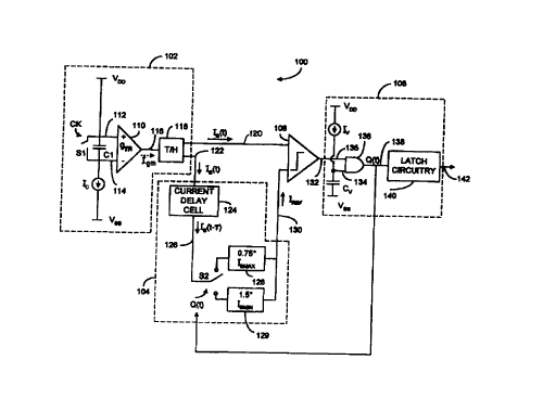
Decoder circuit 100 includes current generator
10 102, reference current generator 104, edge triggered
comparator 106 and output circuitry 108. Current
generator 102 includes switch S1, capacitor C1, current
sink I~, transconductance amplifier stage 110 and track
and hold circuit 118. Input 112 of transconductance
15 amplifier 110 is coupled to supply voltage
Capacitor C1 and switch Sl are coupled in parallel
across inputs 112 and 114 of amplifier 110. Current
sink I~ is coupled between input 114 of amplifier 110
and supply voltage VSS. Output 116 of amplifier 110
20 provides current Igm as an input to track and hold
circuit 118. Track and hold circuit 118 provides at
outputs 120 and 122 currents IS(t) which are delayed
versions of Igm.
Switch S1 is controlled using the incoming
25 encoded data signal CK. During the high voltage
portions of the CK signal duty cycle, switch S1 opens.
Switch S1, capacitor C1, current sink I~ and
transconductance amplifier 110 together form super
linear integration circuit. The term, "super linear" is
30 intended to indicate that the output of the integration
circuit as a function of time can be represented by y =
mt" (where X is greater than one). Depending upon the
period or frequency of incoming signal CK controlling
switch S1, output current Ig", at output 116 of amplifier
CA 02305425 2000-03-30
WO 99/17508 PCTIUS98/20274
-11-
110 will have one of two period or frequency dependent
final values, with each final value corresponding to one
of the two data states encoded. However, in other
embodiments, the circuit can be adapted to provide three
5 or more output states corresponding to .three or more
possible data states.
Track and hold circuit 118 maintains current
Ig", during the low voltage portions of the CK signal
duty cycle such that output current I9(t) of track and
10 hold circuit 118 is maintained substantially the same as
I9m during the low voltage portion of the CK signal.
Track and hold circuit 118 is implemented using a
switched current mirror of the type which maintains the
output current even after the input current has changed.
15 Alternatively, a voltage type sample and hold (S/H)
circuit can be used. Output current IS(t) from circuit
118 is provided to comparator 106 at input 120, and to
reference current generator 104 at input 122. Thus,
current Ia(t) is mirrored such that it can be provided
20 at two track and hold circuit outputs. Operation of
current generator 102 is discussed and shown in further
detail with reference to FIG.s 5 and 6. However, for
ease of illustration, only generation of one IS(t)
output current is shown in FIG.s 5 and 6.
25 Reference current generator 104 generates a
reference current I~F which is provided to edge
triggered comparator 106 for comparison to current
I8(t). With current I~ appropriately adjusted,
reference current generator 104 generates a
30 substantially constant reference current for any given
set of encoded input signal frequencies, and
automatically adjusts the reference current
appropriately if I$ (t) varies slightly due to process or
temperature. Reference current generator 104 includes
CA 02305425 2000-03-30
WO 99/17508 PCT/US98/20274
-12-
current delay cell 124, switch SZ, multiplier circuit
128 and multiplier circuit 129. Current delay cell 124
can be a switched current mirror or other well known
circuits which receive as am input current IS(t), which
5 maintain that-input current for a period of time T, and
then provide at a later time substantially the same
current as IS(t-T). Thus, current delay cell 124
provides at its output 126 a current approximately equal
to current IS (t) from the previous cycle of the incoming
10 encoded data signal CK. Generally, T will have one of
two values depending upon the sequence of data states
received by decoder 100. When the previous and current
bits each represent logical "0" data states, T will be
approximately equal to To. When the previous and
15 current bits each represent logical "1" data states, T
will be approximately equal to T1. When the previous
and current bits represent a transition from a logical
"1" data state to a logical "0" data state, or vice
versa, z will be approximately equal to 1/2*(To + Tl).
20 Depending upon output Q(t) of decoder 100
(discussed below in greater detail), switch SZ couples
output 126 of current delay cell 124 to one of
multiplier circuits 128 and 129. If selected,
multiplier circuit 128 multiplies current IS(t-T) by
25 0.75, while multiplier circuit 129 multiplies current
IS(t-T) by 1.5. Other multiplication factors can be
used if frequencies other than 900 MHz and 1.8 MHz are
used to encode the data in the high accuracy mode of
operation, for example. Large variations in Ie(t), as
30 would occur when switching between the high accuracy and
low power frequency ranges, are prevented or
accommodated by controlling current I~ in order to
change the integration rate of the super linear
CA 02305425 2000-03-30
WO 99/17508 PCT/US98/20274
-13-
integrator. Generally, I~ is controlled so that current
IB(t) is nominally always at about the same value.
The minimum value ISMIN of current IS ( t )
provided from current generator 102 (corresponding to
5 period To and-therefore to a logical "0" or first data
state) is preferably set to approximately one half of
the maximum current value IS,,,~ of current IS ( t
(corresponding to period Tl and therefore to a logical
"1" or second data state) . Therefore, reference current
10 I~F at output 130 of reference current generator 104
will be substantially constant as shown in equation 1:
I,~F ( for all t ) =1. 5 * ISMIN = ~ . 75 * IS,"~ Eq . 1
15 Because comparator 106 is edge triggered,
output Q (t) will correspond to the previous encoded bit
until the comparator again latches. Therefore, with
current delay cell 124 also providing current Ie(t-z)
corresponding to the previous decoded bit, switch 52 is
20 controlled such that the correct multiplication circuit
is chosen to provide reference current IREF. One
advantage of decoder circuit 100 is that current I~ can
be controlled so that current generator 104 provides an
appropriate reference current regardless of the
25 particular set of periods (and therefore regardless of
the possible values of ISMIN and IS,"~) chosen to represent
the logic levels in the data stream. The reference
current IasF is maintained during slight variations in
Ie(t), caused by temperature or process variations, by
30 the appropriate selection of multipliers 128 and 129.
This provides advantages in that, with little or no
circuit modification, decoder circuit 100 can be used to
decode signals encoded with any of a wide range of sets
of periods. This adaptability, along with I~
CA 02305425 2000-03-30
WO 99/17508 PCT/US98/20274
-14-
modification, allows the periods to be selected or
changed as may be convenient or necessary without
modifying circuit 100. The ability to tailor the signal
periods without modifying the circuitry saves time and
5 costs. The use of multiplication circuits 128 and 129
allows an adequate reference current to be generated
when small variations in the incoming data or clock
signal CK occur.
Current comparator 106 receives current IS(t)
10 from output 120 of current generator 102 at one of its
inputs. Current comparator 106 receives at its other
input reference current IRSF from output 130 of reference
current generator 104. At output 132, comparator 106
provides a high or low voltage output, depending upon
15 whether current IS(t) is greater or lesser than
reference current IREF. Thus, comparator output 132 is
indicative of whether a particular bit of the encoded
signal received at switch S1 contained an encoded "1" or
a "0".
20 The output voltage signal at output 132 of
comparator 106 is provided to output circuitry 108. It
must be noted that, while comparator 106 is preferably
a current comparator, all or parts of decoder circuit
100 can be implemented using voltage mode circuits
25 instead of current mode circuits. For example, current
generator 102 can be replaced by a voltage generating
circuit. Likewise, reference current generator 104
could be replaced with a reference voltage generator
circuit. In this case, comparator 106 would be replaced
30 with a voltage comparator circuit. However, due to the
noise immunity and reduced power requirements of current
mode circuits, current-mode circuits such as those
illustrated in FIG. 3 are preferred.
CA 02305425 2000-03-30
WO 99/17508 PCT/US98/20274
-15-
Output circuit 108 includes current source I~,
capacitor C", AND gate 136, and latch circuitry 140.
Current source I" is coupled between supply voltage VDD
and input 134 to AND gate 136. Input 134 to AND gate
5 136 is also coupled through capacitor C~ to supply
voltage VSS. Output 132 of comparator 106 is coupled to
input 135 to AND gate 136. Output signal Q(t) of AND
gate 136 is provided at input 138 to latch circuitry
140. Latch circuitry 140 provides an output at 142
10 which is representative of the state of the data stream
encoded in signal CK. Current source I" and capacitor
C~ cooperate to maintain input 134 of AND gate 136 at a
low logic level voltage immediately after a reset or at
start-up. Thus, output Q(t) is held low for several
15 cycles after start-up until capacitor C" sufficiently
charges. This prevents false outputs due to noise or
other power-up process conditions. In the alternative,
instead of using the delay circuit formed by current
source I" and capacitor C", a power on reset circuit can
20 be used to drive input node 134 of AND gate 136.
After capacitor C~ is sufficiently charged,
output Q(t) will reflect the state of the output of
comparator 106. Latch circuitry 140 receives AND gate
output Q ( t ) as an input and provides an output at output
25 142. Latch 140 is used to latch the individual decoded
bits, corresponding to the encoded bits received in the
serial data stream CK, to other circuitry in the
transmitter.
FIG. 4 is a timing diagram which illustrates
30 output Q(t) as a function of input signal CK. FIG. 4
illustrates the decoded bit (in signal Q(t)) for each
bit or cycle of the period encoded data signal CK.
Output Q(t) changes to its corresponding value for each
bit of encoded signal CK at midpoint (or falling edge
CA 02305425 2000-03-30
WO 99/17508 PCT/US98/20274
-16-
402) of the corresponding received period encoded bit.
Thus, during a transition from a received period encoded
"0" to a received period encoded "1", Q(t) transitions
(at rising edge 404 ) from a "0" to "1" at midpoint ( i . a .
5 falling edge 402) of the received period encoded "1"
bit. While in the preferred implementation of the
present invention Q(t) transitions at the falling edges
of the corresponding bit of the received period encoded
signal, numerous other implementations are possible.
10 For example, Q(t) can be designed to transition at the
start (rising edge 406) of the next encoded bit
received.
FIG. 5 is a circuit diagram which illustrates
current generator 102 in greater detail. As shown in
15 FIG. 5, current generator 102 is divided functionally
into super-linear integration circuit 502 and track and
hold circuit 118. Integration circuit 502 includes
switch S1, capacitor C1, current source I~ and
transconductance amplifier 110. As shown in FIG. 5,
20 transconductance amplifier 110 includes transistors Q,"a,,l
and Q~,Z and current source ID, configured as a
differential amplifier. Transconductance amplifier 110
cooperates with switch S1, capacitor C1 and current
source I~ to form a super-linear integration circuit
25 which provides an output current Igm having a magnitude
which is dependent upon the period length of the cycle
of the encoded input signal CK. Current source I1 is
included to provide a low level current in order to keep
transistor Q~,2 turned on. Track and hold circuit 118
30 includes transistors QMpl and QMP2, capacitor C2, and
reset switch S3. Transistors QMpl, transistor QMp2,
capacitor C2 and switch S3 are configured as a switched
current mirror.
CA 02305425 2000-03-30
WO 99/17508 PCT/US98/20274
-17-
Current generator 102 functions generally as
follows. During the high voltage portion of each
encoded cycle or bit of signal CK, switch S1 is opened.
During this time, capacitor C1 charges and voltage V1
5 drops. Thus, with the control node of transistor Q,;a,,2
coupled to voltage source VDD, a voltage differential
develops between the control nodes of transistors Q,"Q,1
and Q,"Q,2, causing a greater portion of current ID to pass
through transistor Q,"~2. Since turn-on current I1 is
10 very small as compared to current ID, the current
flowing through transistor Q,,Q,2 will be close in
magnitude to that of current Ice, which flows into
transistor QMpl of track and hold circuit 118.
In general, switch S3 is closed when switch Sl
15 is open and vice versa. As illustrated, both switches
Sl and S3 are PMOS type switches. However, other switch
types can be used with slight modifications. In the
embodiment shown, during the high voltage portion of
input signal CK, switch S3 closes, and track and hold
20 circuit 118 operates as a current mirror. Thus current
IS flowing through transistor QMpz will be approximately
equal to current I9m. During the low voltage portion of
each cycle or bit of signal CK, switch S3 opens and the
charge on capacitor CZ keeps transistor QMpz conducting
25 so that output current IS is maintained, even as current
Igm changes. Thus, this switched current mirror design
maintains the current generated by transconductance
stage 110 for use during the next half cycle. Switched
current mirrors of the type used for track and hold
30 device 118 can also be used as current delay cell 124.
FIG. 6 illustrates the correspondence between
current IS from current generator 102 and the incoming
encoded signal CK. As can be seen in FIG. 6, after
falling edge 605 of first cycle 602 (having period Tfl
CA 02305425 2000-03-30
WO 99/17508 PCT/US98/20274
-18-
corresponding to a "0" bit) is received in the encoded
signal CK, current IS takes on its minimum active
current value ISMIN~ At rising edge 606 of next cycle
604 (having period T1 corresponding to "1" bit) of
5 signal CK, Is~drops to substantially zero. At falling
edge 607 of cycle 604, current IS takes on its maximum
value IS,,,~,~. This continues for each bit or cycle of
incoming data signal CK, with current IS taking on
either value ISMIN or value IS,"~. Track and hold circuit
10 118 maintains the current value (either at IsMIN or at
IS,"~) for the remainder of the cycle of the encoded bit .
After the rising edge of the next encoded bit, switch S3
causes current IS to reset to 0.
FIG. 7 illustrates one preferred embodiment of
15 modulator 30 used in accordance with the present
invention to frequency or period encode signals for
transmission across isolator 20. Modulator 30 includes
a clock signal CLOCK having approximately a 50 percent
duty cycle, frequency divider 702 and multiplexes 706.
20 The 50 percent duty cycle clock signal CLOCK can have,
for example, the frequency Fo corresponding to
transmission of a logical 0 bit. This clock signal is
provided both to input 703 of frequency divider 702 and
input 708 of multiplexes 706. After frequency division
25 by divider 702, a signal having a 50 percent duty cycle
but approximately one-half the frequency of clock signal
CLOCK (i.e., having frequency Fl) is provided to
multiplexes 706 at input 704. Using the control signal
input 710 of multiplexes 706, output 712 of multiplexes
30 706 is selectively connected to the appropriate one of
inputs 704 and 708 during each individual cycle. In
this manner, a frequency encoded signal having a duty
cycle of approximately 50 percent can be generated at
output 712.
CA 02305425 2000-03-30
WO 99/17508 PCT/US98/20274
-19-
The present invention provides numerous
advantages over the prior art. For example, the use of
a super linear integration circuit helps to increase the
integrated signal difference between encoded bits of the
5 first and second data states. This in turn provides
greater noise immunity and reduces the likelihood that
transmission errors will occur. Also, preferred
embodiments of the present invention require only a
single integration circuit. The single integration
10 channel nature of the decoder of the present invention
reduces complexity and costs as compared to prior art
two integration channel decoders. Further, use of a
fifty percent duty cycle signal to encode the
transmitted data reduces heat generation, reduces data
15 losses and errors caused by distorted signals from
saturated barrier transformers, and decreases
interference with nearby components which can sometimes
result from harmonics in non-fifty percent duty cycle
signals. Additionally, fifty percent duty cycle signals
20 decrease the decoder circuit complexity and increase the
ease at which the encoded signal is generated.
The methods and circuits of the present
invention can be implemented using various hardware,
software and hardware/software combinations to encode
25 and decode the data signals in order to transmit and
receive messages. The present invention is particularly
well adapted for use in process control transmitters,
valve controllers, and in process control field devices
in general because of the low current consumption of the
30 present invention. As used herein, the term process
control instrument is intended to mean any of these and
other process control devices. However, the present
invention can be utilized in any of a wide variety of
applications in which devices on a printed circuit board
CA 02305425 2000-03-30
' ~ ' - - , , . , ,, ,., ,,,, ,.,
~ WO 99/17508 ' ~' , ' , ' ' ~ ~ pt::'1'/L~.S48/2(3274
- " - ~ . -
' . " ~ n a O ., n n n ~ v
, ~ a
. _ ~ .. ., n ~ ~
-20-
or coupled to a data line in general are required to
communicate with each other.
While the present invention is described
primarily with respect to encoding and decoding logical
ones and zeros, the present invention can also be used
to implement multi-state communications in which more
than two data states are encoded. The single super
linear integration circuit and other decoding circuitry
can be used to decode either pulse width modulated or
frequency modulated signals with little or no
modification. Terms such as decoding circuitry,
integration circuitry and current generator circuitry
can all be used to refer to transition detecting
circuitry of the type which detects transitions in an
encoded signal for purposes of decoding the signal.
A!J~ND~D S~!~~T