Note: Descriptions are shown in the official language in which they were submitted.
CA 02305523 2000-04-03
WO 00/14721 PCT/US99/19128
Description
SOUND-PRODUCING INTEGRATED CIRCUIT WITH VIRTUAL CACHE
TECHNICAL FIELD
The present invention relates to electrical
musical tone generation, and particularly to digital
audio signal processing systems that employ digital audio
sample memory and data cache memory for use by the
processing systems in sound synthesis.
BACKGROUND ART
The increasing use of MIDI and music synthesis
capabilities in electronic musical instruments, Karaoke
and PC multimedia applications is fueling the demand for
high performance, yet cost effective, sound production
systems. Digital sound synthesizing and processing
systems make use of digital audio sample memory for a
variety of purposes, including as a wavetable memory
storing audio samples for synthesizing sounds, as a delay
buffer memory for reverb and chorusing effects process-
ing, and as a streaming audio memory receiving audio
samples from external audio inputs such as a music
keyboard, microphone, or the hard disk of multimedia PC.
Such systems also employ a data cache memory in order to
reduce the number of required accesses of the sample
memory, and thereby minimize bottlenecks in this time-
critical environment. One example of an audio signal
processor integrated circuit architecture for music
synthesis applications is described by Chris Deforeit et
al., in a paper entitled "A Music Synthesizer Architec-
ture which Integrates a Specialized DSP Core and a 16-bit
Microprocessor on a Single Chip", presented at the 98th
Convention of the Audio Engineering Society (AES) on
February 25, 1995. It has been embodied in the SAM9407
integrated sound studio circuit sold by Dream S.A. of
Semur-en-Auxois, France, a subsidiary of Atmel
CA 02305523 2000-04-03
WO 00114721 PCT/US99/19128 ,
-2-
Corporation of San Jose, California, the assignee of the
present invention.
The aforementioned circuit architecture
combines a synthesis digital signal processor (DSP) core,
a control processor, a memory management unit, and
peripheral I/O interface logic on a single chip. The
synthesis DSP is constructed with hardware that has been
optimized for the music synthesis task, and by repeatedly
and efficiently performing a limited number of operations
needed to carry out synthesis-specific algorithms, it
directly generates and processes up to 64 simultaneous
voices using the digital audio sample data accessed from
external sample memory. The DSP synthesis algorithms are
stored in on-chip program memory, while parameter data
for the synthesized voices are stored in blocks of on-
chip parameter memory. The control processor interfaces
with external peripheral devices, such as a host computer
or MIDI keyboard, through the peripheral I/O logic. The
control processor parses and interprets incoming commands
and data from such peripheral devices, and then controls
the synthesis DSP by writing into the DSP's parameter
memory. Besides these command parsing and control tasks,
the control processor can also perform slowly changing
synthesis operations, such as low frequency oscillation
and waveform envelope management, by periodically
updating synthesis parameters in the parameter memory.
The memory management unit allows external memory
resources to be shared by both the control processor and
synthesis DSP. Thus, for example, a single external ROM
device may serve as both program memory for the control
processor and sample memory for the DSP, and a single
external RAM device may serve as both external data
memory for the control processor and delay buffer memory
for the effects processing done by the DSP.
The synthesis DSP operates on a frame timing
basis with each synthesis frame divided into several
process slots (e.g., 64 slots in the aforementioned SAM
9407 device). A 'process' relates to an elementary sound
CA 02305523 2000-04-03
WO 00/14721 PCT/US99/19128 ,
-3-
production function, such as one voice wavetable
synthesis, one delay line for effects, etc., and each
process generally involves reading or writing one or more
audio samples from or to the digital audio sample memory.
The maximum number of processes that can be executed
within one synthesis frame (i.e., the number of slots)
determines the capability of the device. For example, if
all process slots were dedicated to wavetable synthesis,
the number of slots would be the maximum polyphony
(although slots might also be linked together to
implement more complex synthesis algorithms). Also, some
number of slots (e. g., eight) may be required fof effects
processing, leaving fewer slots available for polyphonic
wavetable sound synthesis.
It is desirable to increase the number of
processing slots per synthesis frame. Because each
processing slot typically requires at least two digital
audio sample memory accessed per frame, a 128 slot device
would need 256 or more accesses per frame. With a state
of the art frame rate of 48 kHz, this leads to sample
memory cycles of at most 81 ns. Fortunately, in most
cases, the same audio sample has to be accessed on
successive frames. Thus, potential traffic bottlenecks
between the synthesis DSP and the sample memory can be
avoided by using an on-chip data cache memory to minimize
the number of sample memory accesses that are needed. In
a straightforward implementation, where the data cache
has memory space for at least two audio samples allocated
to each slot, the cache memory size in samples is at
least twice the number of slots. With a typical audio
sample width of about 16 or 24 bits, the data cache would
need to hold a minimum of 4 or 6 kbits for a 128-slot
device.
However, it is further desirable in a
multimedia PC environment for the digital audio sample
memory to share the PC's main memory instead of using
separate ROM and RAM. But, the structure of modern PC
buses (such as PCI) uses a memory word width of 256 bits
CA 02305523 2000-04-03
WO 00/14721 PCT/US99/19128 _
-4-
(referred to as a PC cache line). Thus, a regular imple-
mentation of a synthesis DSP's data cache memory usable
in such a PC memory sharing environment would require two
PC cache lines per processing slot, and hence a size of
at least 64 kbits of on-chip cache for a 128-slot device.
It is an object of the present invention to
implement an improvement in cache memory organization for
sound synthesis DSP applications that results in a
significant reduction in the required size of the data
l0 cache memory.
It is another object of the present invention
to optimize the synthesis DSP cache management to the
large cache line structure of modern PC buses in order to
improve transfers of audio sample data between the sample
memory located on the PC's main board and the on-chip
data cache memory.
It is a further object of the invention to
provide for variable digital audio sample memory word
sizes.
DISCLOSURE OF THE INVENTION
These objectives are met by a digital sound
producing integrated circuit device that uses external
sample memory for storing digital audio data samples,
wherein the on-chip data cache memory organization is not
correlated to the synthesis slots, but rather employs an
additional virtual cache memory to dynamically allocate
real data cache memory lines to the various slots, as
needed.
In particular, the digital sound-producing
device includes a digital signal processor (DSP) core
that requests access to the sample memory by supplying a
virtual address to a virtual cache memory block. The
device also includes a data cache memory in a data path
between the DSP and the sample memory. The data cache
memory stores, in cache lines thereof, audio sample data,
including data that has been read from the sample memory
for use by the DSP and data that has been written thereto
CA 02305523 2000-04-03
WO 00/14721 PCT/US99/19128 _
-5-
by the DSP. The device further includes the afore-
mentioned virtual cache memory block, which is located in
an address path between the DSP and both the sample
memory and the data cache memory. The virtual cache
memory block receives the virtual addresses from the DSP
requesting access to the sample memory, and determines
whether that address already corresponds to an allocated
cache line of the data cache memory. If not, it allo-
cates a new cache line as corresponding to the virtual
memory and addresses the sample memory for transfer of
the audio sample data to the cache line. The data is
available to the DSP during the next processing frame.
If a cache line corresponding to the virtual address has
already been allocated, the virtual cache memory block
addresses the data cache memory for transfer of audio
sample data between that corresponding cache line and the
DSP. The virtual cache memory block also de-allocates
cache lines not used in the current or previous frame,
addressing the sample memory for transfer of the audio
sample from the data cache to the sample memory. The
virtual cache memory block includes a data line table
storing, for each virtual address, the corresponding
allocated data cache address, and also includes a virtual
cache address table and other circuitry for processing
current access requests, as described in further detail
below.
The sample memory can be a RoM or flash memory,
a RAM or DRAM, and may be indirectly accessed through a
PC bus. A cache line transfer between the sample memory
and the data cache memory may consist of a burst of
several access (read or write) cycles. For example,
where the data cache memory is a DRAM, the transfer may
be a burst of several DRAM fast page mode access cycles.
The audio sample data blocks stored in the data cache
memory may match the cache line size for a personal
computer (PC) or the audio samples can have different
sizes in various cache lines of the data cache.
Likewise, the data read by the DSP from the data cache
CA 02305523 2000-04-03
WO 00/14721 PCT/US99/19128 _
-6-
can have a variable number of bits, as requested by the
DSP. The virtual address provided by the DSP may be the
same as the corresponding sample memory address. Alter-
natively, the virtual cache memory block could access the
sample memory by shifting the received virtual address by
a quantity commensurate with the audio sample word size
and adding the result of that shift to a base register
(or several base registers) to provide the sample memory
address. The virtual cache memory block can also handle
any data cache memory full situations by providing the
previous audio sample, instead of no sample, and thus
avoid audio clicking.
BRIEF DESCRIPTION OF THE DRAWINGS
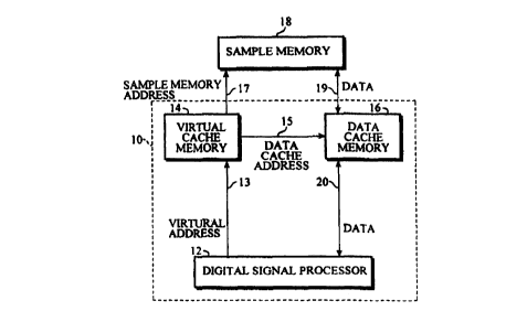
Fig. 1 is a schematic block diagram of a
digital sound-producing integrated circuit device of the
present invention together with an external sample
memory, with the address and data paths shown.
Fig. 2 is a schematic block diagram of a data
cache memory in the device of Fig. 1 together with
associated input/output selection elements therefor.
Fig. 3 is a schematic block diagram detailing a
virtual cache memory block in the device of Fig. 1.
Fig. 4 is a schematic block diagram further
detailing a DSP-cache interface in the virtual cache
memory block of Fig. 3.
BEST MODE OF CARRYING OUT THE INVENTION
With reference to Fig. 1, that portion of the
digital sound producing integrated circuit l0 that is
responsible for synthesizing and processing an audio
signal, namely the digital signal processor (DSP) core
12, and for interfacing the DSP with an external digital
audio sample memory 18, namely the cache memory structure
of the present invention combining a data cache memory 16
with a virtual cache memory 14, is shown together with
their main address and data paths. For the sake of
clarity, control signals are omitted from this figure.
CA 02305523 2000-04-03
WO 00/14721 PCT/US99/19128
-7-
The sample memory 18 stores successions of
individual audio samples as an audio stream. For a given
audio stream, the samples might be 8, 16 or 32 bits wide,
and can be organized in a multichannel interleaved way.
The sample memory 18 is represented as a conventional
functional block only and will not be further detailed.
It is essentially the same as any of those used in prior
sound synthesis applications. For example, it could be a
ROM or DRAM device, or it might be the memory of a
personal computer (PC), accessed from a PC cache memory
through a PCI bus. It is accessed via data I/O lines 19
by the sound chip 10 by providing a sample memory address
on chip output lines 17.
The DSP core 12 provides an address correspond-
ing to an audio sample on an address line 13, together
with a read or write request, to a virtual cache memory
block 14. Because the DSP 12 does not in the present
invention directly address either sample memory 18 or
data cache memory 16, the address on bus 13 is referred
to as a 'virtual' address, which is used by the virtual
cache memory block 14 to determine the appropriate real
address of either memory 16 or 18. In the case of a
write request, the DSP 12 also provides the actual data
to be written on a data bus 20 connected to the data
cache memory 16.
The virtual cache memory 14 receives the
virtual address on bus 13 from the DSP 12 and allocates a
new or already existing data cache address corresponding
to a cache line of the data cache memory 16. (Details
for this allocation will be explained below.) At this
point, if a read operation has been requested by the DSP
12, the virtual cache memory block 14 will decide whether
the audio sample data can be read directly from the on-
chip data cache 16 or if an access to the external sample
memory 18 is necessary. If access to the sample memory
18 is necessary, the virtual cache memory 14 will cal-
culate a sample memory address from the received virtual
address, the contents of one or more base registers
CA 02305523 2000-04-03
WO 00/14721 PCT/U599/19128
-g-
(optional) and the sample width. It will then provide
the sample memory address over external address bus lines
17 to the sample memory 18 and initiate a sample memory
to data cache line write cycle, which will transfer data
read from the sample memory 18 over data lines 19 to the
allocated data cache memory line indicated by a data
cache address applied on bus 15. If the requested data
is already stored in the allocated cache line, then no
access to the sample memory 18 is necessary and the
requested data will be made available to the DSP 12 over
data bus 20 on the next synthesis frame. If a write
request has been requested by the DSP 12, the audio
sample provided on data bus 20 from the DSP 12 will be
stored into the allocated data cache line of the data
cache 16, as indicated by the data cache address provided
on bus 15 from the virtual cache 14 to the data cache
memory 16. (The write from the data cache 16 to the
sample memory 18 will be explained later.)
With reference to Fig. 2, the data cache memory
block 16 preferably has a cache line width of 256 bits
and a bus width for data bus 19 to or from the sample
memory of 32 bits, as is typical for PC memory sharing
applications through a standard PCI bus. However, any
other size cache line and bus width can be designed as
long as one cache line can store at least one audio
sample. As is seen for the preferred 256-bit cache line
size, one cache line can hold either 32 8-bit audio
samples (represented by cache line 21), 16 16-bit audio
samples (cache line 22) or 8 32-bit audio samples (cache
line 23). The sample width selection is controlled from
the DSP to the virtual cache memory. The data cache
memory 16 can be implemented as a single-port SRAM, as
shown. Alternatively, it may be implemented with dual-
port RAM for optimum performance when communicating with
fast PC buses.
The data cache memory 16 receives an address on
bus 15 from the virtual cache memory block and reads (or
writes) sample data from (or to) either the audio sample
CA 02305523 2000-04-03
WO 00/14721 PC'T/US99/19128 ,
-g-
memory through a PCI data bus 19 or the DSP through data
bus 20. Selection of bus 19 or 20 is controlled by the
virtual cache memory block through a multiplexer 24.
When communicating with the PCI bus 19, a full 256-bit
cache line is read (or written) using a burst mode of 8
32-bit transfers, using a multiplexer 31 with control
inputs 30. This way of making such a transfer is well
known to those skilled in the art and fully detailed in
the PCI bus specification. When communicating with the
DSP through data bus 20, the audio sample transfers occur
on an individual audio sample basis, which can be 8, 16,
or 32 bits wide. These transfers are controlled by the
virtual cache memory block using control signals 26 and
28. In particular, when reading the data cache 16, the
correct audio sample is selected by means of multiplexers
27 and 29. When writing to the data cache 16, two
implementations are possible. Either a read/modify/write
cycle can be used to store the audio sample at the
correct position in the cache line, or several write
enable signals to the data cache memory can enable
modification of only the necessary portion of the stored
cache line.
With reference to Fig. 3, the virtual cache
memory block 14 includes a DSP-cache interface 33. The
interface 33 has signal inputs 13 and 35-37 receiving,
respectively, the virtual address, the current processing
slot number, the current access request number for the
current slot, and the current read/write request number
for the current slot. Each of these inputs is connected
to corresponding outputs from the DSP. The interface 33
also has signal outputs 39, 41 and 45 connected to a
virtual cache address table 43 and a virtual cache data
line table 47. When requesting access, the interface 33
provides a virtual cache address vn signal lines 39
addressing the virtual cache address table 43 and the
virtual address on lines 41 to data inputs of the address
table 43. When accessing data in a read or write opera-
tion, the interface 33 provides the current DSP virtual
CA 02305523 2000-04-03
WO 00/14721 PCTNS99/19128,
-10-
cache address to the virtual cache data line table 47 in
order to retrieve the stored corresponding data cache
address.
The virtual cache memory block 14 also includes
a virtual cache address table 43. The size of this table
corresponds to the maximum of sample memory accesses that
can be performed within a single frame. It holds, for
each possible access, the current virtual address
(VADDR), a valid bit (V), and a request bit (R) that
indicates whether that virtual address is actually
requesting access. For technology reasons, the virtual
cache address table 43 is preferably made up of two
devices, namely a random access memory or RAM that holds
the virtual address byte (VADDR) and the valid bit (V),
and a register bank that holds the request bits (R). In
one implementation, the current virtual address (VADDR)
is sent as the sample memory address on address lines 17.
An equality comparator 49 compares the incoming virtual
address 41 from the interface 33 to the virtual address
(VADDR) stored in the virtual cache address table 43 that
is output on lines 17. This comparison is performed with
the lower 5 bits masked, therefore indicating to the
cache manager 71 whether the requested data is already
present in a cache line of the data cache.
A priority encoder 51 receives all request bits
(R) in parallel from the register bank of the virtual
cache address table 43. It determines which virtual
cache address (VCADDR) is requesting service (R = 1).
The priority encoder 51 outputs that virtual cache
address (VCADDR) to an increment/decrement device 55 that
outputs either VCADDR-1, VCADDR, or VCADDR+1, as
determined by control signals (*) from the cache manager
71. That output 57 in turn accesses both the virtual
cache address table 43 and the virtual cache data line
table 47. Therefore, it is possible from a given virtual
cache address (VCADDR) to also read the previous or next
virtual cache address as well. The virtual addresses
read from these previous and next virtual cache
CA 02305523 2000-04-03
WO 00/14721 PCT/US99/19128
-11-
addresses, with the lower 5 bits masked, can be stored,
respectively, into two registers 59 and 60. Two equality
comparators 61 and 62 compare these virtual addresses,
with the lower 5 bits masked, with the corresponding
current virtual address from the cache address table 43
to determine whether the addresses refer to the same data
cache line, and indicate this to the cache manager 71.
The virtual cache memory block 14 also includes
a virtual cache data line table 47. This table, which
can be implemented as standard RAM, has the same size as
the virtual cache address table 43. It holds, for each
active entry, the address (DCADDR) of the corresponding
cache line of the data cache. To allocate a free data
cache line, two register banks 65 and 66 and a priority
encoder 67 is used. Each "in-use" register bank 65 and
66, for the current FRAME and previous FRAME-1, has a
size equal to the number of storage locations of the
tables 43 and 47. Each bit of these register banks
indicates that the corresponding data cache line is
already in use. The priority encoder 67 indicates which
is the first register bit set at zero (free or not in
use), and therefore the priority encoder's output is the
first available data cache address (DCADDR) that can be
assigned to correspond to a virtual address.
A cache manager block 71 is used to sequence
all operations concerning a request from the virtual
cache address table 43. The cache manager 71 receives
information from various elements 43, 49, 61 and 62 of
the block 14 of Fig. 3, and sequentially generates
control signals. The cache manager 71 can be implemented
using a microprogram, a PLA, or a truth table decoded
with gates, as is well known in the art. Operation of
the virtual cache memory block 14 will be further
described below.
With reference to Fig. 4, the DSP cache
interface 33 of Fig. 3 includes a virtual cache
configuration table 75, a first-in first out (FIFO)
memory 91, adders 81 and 100 and a multiplexer 87. The
CA 02305523 2000-04-03
WO 00/14721 PCT/US99/19128
-12-
configuration table 75 is equal in size to the number of
processing slots from the DSP. It receives the current
slot number from the DSP on input lines 35. For each
slot, it indicates in a field 77 the first virtual cache
address (1st Vcache) that should be used, as well as
indicating in a field 79 the successive read or write
operations (R/W) to be performed within one slot. The
number of individual bits in the field 79 to indicate
such successive operations is equal to the maximum number
of memory accesses that can be performed within one slot
(e. g., four in the depicted implementation). The virtual
cache configuration table 75 is loaded once by the DSP
for a given synthesis/processing configuration. If an
application uses a fixed configuration, then the table 75
can be implemented as ROM.
When requesting a sample memory access, the DSP
provides, besides the slot number on input 35, the
virtual address (VADDR) for the access on input 13 (to
the FIFO memory 91), and the access request number within
the slot on input 36. The adder 81 adds the access
request number to the slot s first virtual cache address
(1st Vcache) received on line 78 from the field 77 of the
configuration table 75 to provide on line 83 a current
virtual cache address (VCADDR) to the FIFO memory 91.
The individual read/write access bits (R/W) in field 79
of the configuration table 75 are output on line 85 and
selected by multiplexer 87, using the access request
number from input 36 as a selection control signal. The
multiplexer 87 thus provides a bit on output 89 to the
FIFO memory 91 indicating whether this particular access
is a read or a write.
The FIFO memory 91 has fields 93, 95, 97 and 99
respectively storing the current virtual cache address
(VCADDR), the virtual address for the access (VADDR), a
bit indicating whether this is a first request for the
slot (1st RQST), and the read/write bit (R/W) indicating
the type of access requested. The FIFO memory 91 files
all access requests from the DSP and has a size which is
CA 02305523 2000-04-03
WO 00/14721 PCT/US99/19128
-13-
twice the maximum access count for a slot. The virtual
cache address (VCADDR) and the virtual address (VADDR)
together with the corresponding request bits in fields 97
and 99 are provided by the FIFO memory 91 on outputs 39
and 41 for loading into the virtual cache address table
43 in Fig. 3.
When requesting data access, the DSP also
provides the current read/write request number for the
current slot on an input 37, which is added by adder 100
to the first virtual cache address (1st Vcache) received
from the configuration table 75 on lines 78 so as to
provide the current DSP virtual cache address on line 45
to the data line table 47 of Fig. 3.
The operation of the device is best understood
using the following examples. It should be first
understood that all data transfers occur with one DSP
frame delay. That is, the DSP requests access at frame F
and then transfers data at frame F+1. This gives the
virtual cache memory block 14 a full frame to obtain the
requested data from the sample memory. This is parti-
cularly important whenever the sample memory is accessed
through a PCI bus or any other bus in which several
agents may simultaneously request service on the bus.
Read example
We suppose that DSP slot ,#3 wants to access two
successive samples at address 1000H (H means hexadecimal
notation). This is a typical case in synthesis using
linear interpolation (Linear interpolation is the easiest
method to determine the approximate value of an unknown
sample between two consecutive samples. A more accurate
method involves convolution.) Both methods are well
known by those skilled in the art and have been described
in detail in the book "Musical Applications of
Microprocessors" by Hal Chamberlain, Hayden Book Company
1985) .
Referring to Fig. 4, slot ,~3 will access the
Vcache config table 75 providing the first Vcache address
CA 02305523 2000-04-03
WO 00/14721 PCT/US99/19128
-14-
(for example, 10) from field 77. The first two indivi-
dual bits in field 79 would be zero to indicate read
operations. Two writes will occur into the FIFO memory
91 during the slot:
10
First write: Vcache address = 10 ,
Virtual address = 1000H ,
first request = 1 ,
R/W = 0
Second write: Vcache address = il ,
Virtual address = 1001H ,
first request = 0 ,
R/W = 0
During next slot (slot #4), the FIFO memory 91
will be read, until it is empty or a first request bit in
field 97 is set (meaning that the DSP is currently
filling the FIFO during slot #4). After the FIFO read,
the content of the Vcache address table 43 (fig. 3) will
be:
Address 10: virtual address 1000H, VALID = 0, RQST = 1
Address 11: virtual address 1001H, VALID = 0, RQST = 1
At this point we will detail the cache manager
control logic operation from fig. 3. Because RQST bits
have been set, the priority encoder 51 will indicate
Vcache address 10 requesting service. The cache manager
71 will look at the previous Vcache address (9) and the
next Vcache address (11) checking for VALID bits. These
bits not being set, the cache manager will allocate a new
cache data line, by writing the first available data
cache address given by the priority encoder 51 (for
example 3) to the Vcache data line table 47. It will
then execute a sampling memory access burst cycle which
will fill the data cache memory 16 at address 3 (fig. 2)
with a cache line (byte addresses 1000H to 101FH). It
will then set the VALID bit and reset the RQST bit for
Vcache address 10.
CA 02305523 2000-04-03
WO 00/14721 PCT/US99/19128
-15-
The RQST bit from Vcache address 10 being
reset, the priority encoder will indicate Vcache address
11 requesting service. The cache manager 71, looking at
the previous Vcache address (10), will find the VALID bit
set. It will find also that the Vcache address 10 holds
the same virtual address as Vcache address il with the
lower 5 bits masked (Using the R-1 storage 59 and the
equality comparator 61). Consequently it will assign the
same data cache address (3) to Vcache address 11 as
Vcache address 10, by reading the data cache address (3)
from address 10 of Vcache data line table 47 into the
temporary register R and writing R back to Vcache data
line table 47 at address 11. The cache manager 71 will
then set the VALID bit and reset the RQST bit for Vcache
address 11.
Assuming that no other RQST are pending, the
cache manager 71 will enter an idle state until next
frame.
At next frame slot #3, the DSP can now read the
datum requested at previous frame. The slot #3 accesses
the Vcache config table 75 (fig. 4) providing the first
Vcache address (10). The first access (0) added by adder
81 to the first Vcache address provides a DSP Vcache
address 10, which through the Vcache data line table 47
indicates data cache address 3. The data cache is read
at address 3 to provide the correct data to the DSP.
Similarly the second access (1) will read the same data
cache line.
If the virtual addresses do not change, reads
on subsequent frames will always occur from the data
cache. We will now detail two other cases:
- Virtual addresses are incremented
- Virtual addresses cross a cache line boundary.
Virtual addresses are incremented (now 1001H
and 1002H : We start from the FIFO read operation. The
virtual address (VADDR) stored in the Vcache address
table 43 at address 10 (currently 1000H) is compared by
comparator 49 with the incoming virtual address (10o1H)
CA 02305523 2000-04-03
WO 00/14721 PGT/US99/19128
-16-
with the 5 lower bits masked. Therefore, they are found
identical. The VALID bit is then set, and no RQST is
set. Further read operations will occur from the data
cache memory 16 as described before. The same applies to
the Vcache address table 43 at address 11.
Virtual addresses cross a cache line boundary
(now lOlFH and 1020H): Starting from the FIFO read
operation, the virtual address (VADDR) stored in the
Vcache address table 43 at address 10 (currently 1000H)
is compared by comparison circuit 49 With the incoming
virtual address (101FH) with the 5 lower bits masked.
Therefore they are found identical and the first read
will occur from the data cache memory 16 as described
before. The virtual address stored in the Vcache address
table 43 at address 11 (currently 1001H) is compared with
the incoming virtual address (1020H) with the 5 lower
bits masked. They are found different. Therefore, the
incoming virtual address (1020H) is stored into the
Vcache address table 43 at address 11, the valid bit is
reset and the request bit is set. The RQST bit
processing from the cache manager 71 will then allocate a
new cache data line as explained before.
Data cache line allocation and de-allocation principle
A data cache line which is not used within a
processing frame is de-allocated (m~ide free for new
allocation). To do so, two "in-use" register banks 65
and 66 are used, each register bank having the size of
the total number of data cache lines. At the beginning
of each frame, the "in use" register "Frame" 65 is
transferred to the "in use" register "Frame-1" 66 and the
"in use" register "Frame" 65 is cleared. Within a frame,
each time a data cache line is accessed, the correspond-
ing bit from the "in-use" register "Frame" 65 is set.
Therefore, at the end of frame, the "in-use" register
"Frame" 65 has bit sets corresponding to all used cache
lines, and consequently, the "in use" register "Frame-1"
66 is valid within a full frame. The priority encoder 67
CA 02305523 2000-04-03
WO 00/14721 PCT/US99/19128
-17-
connected to the "in use Frame-1" register 66 indicates
the first bit at zero, which is the first available data
cache line.
~lriting~ data to the sample memory
Data write requests from the DSP 12 to the
sample memory 18 are written directly to a data cache
line in the data cache memory 16. A full data cache line
is written to the sample memory 18 when the virtual
address crosses a cache line boundary (for example from
101FH to 1020H). This is detected by the comparison
circuit 49 at FIFO read time when the virtual address
stored in the Vcache address table 43 does not match the
incoming virtual address on lines 41 (with 5 lower bits
masked).
Conversion of virtual address to sample memory address
In a PC environment, it is highly desirable to
compute a sample memory address different from the DSP
virtual address. This allows simple reallocation of PC
memory without having to change the DSP program. Also
this allows handling of interleaved multichannel audio
formats as several monophonic audio streams seen from the
DSP.
In the previous description, the Sample memory
address output on lines 17 (Fig. 3) was identical to the
virtual address (VADDR) provided by the DSP on lines 13.
An improvement consists in computing the sample memory
address (SMA) as follows:
SMA = BASE + {{VA*NCHAN) + CHAN) * BYTESPERCHANNEL
Where VA is the virtual address, SMA the sample memory
address, NCHAN the number of interleaved channels, CHAN
the current channel, BYTESPERCHANNEL the number of bytes
to code one sample on a channel and BASE a register. To
avoid costly multiplications, NCHAN and BYTESPERCHANNEL
can be restricted to be powers of two, then the multi-
plications simply become left shifts.
CA 02305523 2000-04-03
WO 00/14721 PCT/US99/19128
-18-
Another level of sophistication is to have
several BASE registers, selected according to VA
contents. This allows the PC memory to be segmented,
which allows better optimization of the PC memory space.