Note: Descriptions are shown in the official language in which they were submitted.
CA 02305536 2000-03-31
WO 99/18651 PCT/US98/19842
PHASE CONTROLLED DIMMING SYSTEM WITH ACTIVE
FILTER FOR PREVENTING FLICKERING AND
UNDESIRED INTENSITY CHANGES
Field of the Invention
~ The present invention relates generally to electronic systems that employ a
phase control technique to control the amount of power delivered from an AC
source/AC
line to a load, such as a lighting load. The present invention specifically
relates to a
lighting control system, such as a dimming panel or a wall mounted dimmer
switch, that
employs a phase control technique to control the dimming level of a lighting
load by
altering the conduction angle of a thyristor that is in series with the load.
Background of the Invention
The present invention is described herein in the context of a dimming
system for a lighting load, but is not limited thereto. The present invention
has
applicability in any AC phase control system where it is desired to minimize
undesired
variations in the power delivered to a phase controlled load caused by a noisy
or unstable
AC source, especially at low levels of delivered power.
Most lighting control systems that have a dimming capability employ a
thyristor in series with the AC lighting load to effect the dimming function.
Dimming is
performed by altering the conduction angle of the thyristor, usually by
delivering a trigger
signal to a gate of the thyristor such that the timing of the trigger signal
varies with the
selected dimming level. In a typical forward phase control system, generation
of the
trigger signal is synchronized with the AC line voltage (the fundamental
frequency
waveform of which is sometimes referred to herein as "the AC fundamental")
such that,
some time after a zero crossing of the AC line voltage is detected, the
trigger signal is
generated, the gate of the thyristor is energized, and the thyristor conducts
for the
remainder of the AC half cycle. During the time interval between the detection
of the zero
crossing and the generation of the trigger signal, the thyristor is non-
conducting (during
CA 02305536 2006-O1-27
WO 99!18651 PCTIUS98119842
-2-
which time no power is delivered from the AC source to the load), and usually
this time
interval is altered in response to adjustment of a dimming knob or slider by a
user, or_in
response to changes in a dimming signal level. Altering this time interval
thus alters the
conduction angle of the thyristor, and hence alters the RMS power delivered to
the load.
See commonly assigned U.S. Patent Number 5,430,356 entitled "Programunable
Lighting
Control System With Normalized Dimming For Different Light Sources".
At low levels of delivered power (i.e., conduction beginning at phase
angles greater than about 135 ° for each first half cycle, and greater
than about 315 ° for
each second half cycle, of the AC fundamental), even a small variation in the
conduction
angle usually represents a relatively large variation in the percentage of the
total delivered
RMS power. At these low power levels, any variation of the conduction angle,
whether
between AC cycles or over periods of time, can be manifested as annoying and
unacceptable intensity'changes, including visible flickering of the light
source. Since the
conduction angle is dependent on the detection of the zero crossing, it is
crucial that zero
cross detection be accurate and reliable. AC line conditions are rarely ideal,
and less than
ideal conditions can cause inaccuracy in the detection of zero crossings, with
consequent
intensity variations and/or flickering, as well as other problems, especially
at low levels of
delivered power. '
The prior art has recognized that one condition that can cause intensity
variations andlor flickering is intermittent and/or periodic electrical noise
on the AC line.
For example, voltage "spikes" can be imposed on the AC line by the switching
on and off
of heavy equipment such as large motor loads. See Figure 1. Electrical noise
on the AC
line can be incorrectly interpreted by the dimming circuitry as zero crossings
of the AC
fundamental; and these false interpretations can lead to premature andlor
erratic
conduction of the thyristor. The prior art has also recognized that another
condition that
can cause intensity variations and/or flickering is distortion of the AC
waveform, which
can be caused by the mere presence of other loads on the line. Distortion may
be
characterized by a "bumpy" or "wavy" AC waveform, i.e., onethat is not a
smooth
sinusoid. See Figure 2. 'This "bumpiness" can also move relative to the AC
fundamental,
i.e., it is not synchronized to it. Distortion can also cause false zero
crossing detection.
One common prior art solution to the problem of detecting actual zero
crossings in a noisy
CA 02305536 2000-03-31
WO 99/18651- PCT/US98/19842
-3-
and/or distorted AC line is to employ a phase locked loop (PLL) to generate a
signal
internal to the dimming system having a frequency that is intended to track
that of the AC
fundamental. In this system, the internal signal is a new signal generated by
the PLL that
is intended to replicate the AC fundamental. The zero crossings of the
internal signal are
detected, and since it is relatively free of noise and distortion, zero
crossing detection is
relatively straightforward.
The prior art has also recognized (separately from the problems of noise
and distortion) that frequency variations can occur in the AC line. A common
prior art
solution to the problem of detecting zero crossings in an AC line having
unstable
frequency is to sample the AC line during a small "sampling window" (e.g., 500
microsec.
wide) at periodic intervals. In this type of system, known as "window
detection", a sample
timer is set to open the sample window just before the next zero crossing of
the AC line is
expected, e.g., for a 60 Hz line, the sample window is opened at 8.33 msec.
intervals.
During the time that the sample window is open, the AC line is monitored for a
zero
crossing; the AC line is not monitored for zero crossings between sample
windows. Any
zero crossing that is detected after the sample window has been opened can be
taken as the
actual zero crossing of the AC line, and the sample timer is reset. In a prior
art system that
has made and sold by the assignee hereof as the Grafik Eye 4000 Series dimming
panel,
the last zero cross detection is used as the actual zero cross crossing of the
AC line. The
window detection method can detect zero crossings in an AC line of unstable
frequency
provided that the change in period is not so substantial that the actual zero
crossing falls
outside of the sampling window.
The prior art, therefore, has attempted to detect zero crossings by either
operating upon a separately generated signal that is intended to replicate
both the phase
and frequency of the fundamental of the AC line, or by operating upon the AC
line itself.
Another condition that can cause intensity variations and/or flickering is
changes in the RMS voltage of the AC line. Changes in the RMS voltage of the
AC line
can be caused by the presence of harmonics of the AC fundamental on the AC
Line; the
presence of these harmonics changes the shape of the AC line voltage waveform
from a
pure sinusoid to, e.g., a generally sinusoidal waveform having flattened
peaks, rather than
round peaks. See Figure 3. Changes in the RMS voltage of the AC line will
cause
CA 02305536 2000-03-31
WO 991i8651~ PCT/US98/19842
-4-
intensity changes in the lighting load because such changes result in
variations of the total
power delivered to the load, irrespective of when the zero crossings occur.
The prior art has failed to recognize that the conditions of noise/distortion
on the AC line, on the one hand, and frequency variation of the AC line, on
the other hand,
may be simultaneously and/or alternatively present. The prior art has also
failed to
recognize that, in addition to the presence of these conditions, the condition
of changing
RMS voltage may also be simultaneously and/or alternatively present. To make
matters
worse, all of these conditions may be variably and intermittently present on
the AC line,
and these and other Iine conditions may be constantly changing. A condition
that is
present at one moment may be gone or replaced by another at the next moment;
one
combination of conditions may exist at one moment and be replaced by another
combination at the next moment; and/or all or none of these conditions may
exist at any
given time. Thus, in this respect, the condition of the AC line can be
extremely dynamic.
No prior art has attempted to address the problem of detecting zero crossings
in the AC
line under combinations of these conditions, in part, because the prior art
has not
recognized this dynamic nature of the AC line.
The applicants hereof have not only recognized the dynamic nature of the
AC line, but have also recognized why the prior art is incapable of addressing
all of these
conditions. In particular, the applicants hereof have recognized that
conventional
techniques for detecting zero crossings in the presence of noise/distortion
are inconsistent
with conventional techniques for detecting zero crossings in an AC Iine of
unstable
frequency, and that the prior art solutions to these problems conflict. For
example, the
conditions of noise and distortion suggest that the AC line be integrated over
a number of
cycles, and therefore over a period of time, as is done when using a phase
locked loop.
The conditions of frequency changes and changes in RMS voltage, however,
suggest an
instantaneous analysis of the AC line and an instantaneous response to any
frequency or
RMS voltage change. Clearly, invoking a time delay and instantaneous analysis
and
response are conflicting solutions.
The applicants hereof have also discovered that above described PLL and
window detection methods are inconsistent and conflicting solutions.
The PLL method that is effective in a noisy environment is ineffective
when the AC line frequency is unstable, because the PLL effectively employs an
CA 02305536 2000-03-31
PCT/US98/19842
WO 99/18651
-5-
integration technique and frequency changes in the AC line can result in a
temporary
phase shift between the internally generated signal and the AC line. Over
time, the PLL
will adjust the phase of the internal signal to create substantial coincidence
with the AC
line, but during the adjustment time, the conduction angle of the thyristor
will vary and
may be manifested as slow intensity variations in the lighting load. This
condition can be
aggravated if the magnitude and/or rate of frequency variation of the AC line
is greater
than the error correction rate of the PLL, because the PLL may then be unable
to track the
AC line due to timing limits in the software. In this event, the phase
difference between the
AC line and the internal signal will become great, and the intensity of the
light source may
vary significantly. Any time there is a substantial difference between the AC
line zero
cross and the internally generated signal of the PPL for a substantial period
of time, visible
changes in light will occur.
The window detection method that is effective to detect zero crossing in an
AC line of unstable frequency is ineffective in the presence of
noise/distortion because,
when the sample window is open, any zero crossing that occurs, whether due to
noise,
distortion or an actual zero crossing of the AC line, can be taken as the
actual zero crossing
of the AC line. This type of system does not adequately distinguish noise and
distortion
from actual zero crossings, and can possibly aggravate flickering/intensity
variation
problems caused by false detection of zero crossings due to noise/distortion.
Thus, at least in the United States, where the frequency of the AC line
delivered by U.S. electric utility companies has tended to be very stable,
there has been no
substantial need and /or effort to address the issue of frequency change in
the AC line in a
dimming system, and the prior art has tended to focus on the conditions of
noise and
distortion.
Some prior art systems gate the thyristor at regular periodic intervals, based
on a selected dimming level, on the assumption that there will be no change in
the timing
of the zero crossings of the AC fundamental, or in the RMS voltage of the AC
line after
the thyristor has begun conducting. They are designed to deliver what is
assumed will be a
fixed amount of power once conduction begins. In these systems, the problems
caused by
frequency changes and changes in the RMS voltage of the AC line can be
exaggerated.
For example, in a given cycle, both the frequency of the AC line may change
(causing a
change in the time between zero crossings), and, the RMS voltage of the AC
line may
CA 02305536 2000-03-31
WO 99/18651. PCT/US98/19842
-6-
change during conduction. Since, once fired, the thyristor will continue to
conduct until
the next zero crossing occurs, the RMS power delivered to the load can vary
substantially
relative to a preceding or succeeding cycle.
If the integration time of the PLL is made sufficiently large to avoid the
effects of AC line noise, frequency variations as small as 0.2% can be
visible, and in some
locations, especially in some less industrialized countries, the frequency of
the AC line
supplied by the electric company can change substantially more than this over
very short
periods of time.
Software can be employed in a dimming system to analyze the AC
fundamental and address one or more of the above conditions, but a software
based system
can cause other problematic conditions, such as aliasing on the AC line, due
to interaction
between the system's sample clock and the AC line. Aliasing occurs when the
waveform
is under-sampled.
The prior art also includes a dimming system, known as the N-Module, that
has been made and sold by the assignee hereof. A simplified diagram of a
portion of the
N-module is shown in Figure 4. As shown, a transformer T 1 steps down 120VAC
to
24VAC. A 2.2uF capacitor C1 placed across the output of T1, and before the
full wave
bridge rectifier (FWB), combines with the inherent leakage inductance of T1 to
form an
LC filter that reduces or eliminates frequencies above about 1.6 kHz. The
filtered signal is
supplied to the FWB, and the full wave rectified output of the FWB is analyzed
for zero
crossings by a zero crossing detector ZC. The output of ZC is then used for
dimming
purposes. This prior art does not address any of the above discussed problems.
This type
of system will operate satisfactorily when the AC line frequency varies, but
may not
operate properly when the AC line is noisy because the corner frequency is too
high to cut
off noise components in the frequency range 60Hz to 1.6KHz.
The applicants hereof have determined that a solution to the dynamic
problem discussed above requires a system that has both a fast response (for
dealing with
frequency variations in the AC line) and a narrow bandwidth (for eliminating
the effects of
noise and distortion outside the range of the fundamental frequency). The
present
invention is directed to such a solution.
Brief Description of the Drawings
CA 02305536 2000-03-31
PCT/US98119842
WO 99/18651-
Figure 1 is an exemplary plot illustrating the problem of noise spikes on an
AC line in the prior art.
Figure 2 is an exemplary plot illustrating the problem of a "wavy" or
"bumpy" waveform caused by noise on the AC line in the prior art.
Figure 3 is an exemplary plot illustrating the problem of distortion of the
AC line voltage waveform caused by certain conditions in the prior art.
Figure 4 illustrates a relevant portion of a prior art circuit.
Figure 5 illustrates one embodiment of a three wire dimming circuit
employing the present invention.
Figure 6 illustrates another embodiment of a three wire dimming circuit
employing the present invention.
Figure 7 illustrates a two wire embodiment of a dimming circuit employing
the present invention.
Figure 8A illustrates the details of one circuit embodiment of a filter that
may be employed in the practice of the present invention for recovering the AC
fundamental waveform or the second harmonic frequency of the AC fundamental
waveform from the AC line waveform.
Figure 8B is one embodiment of a zero crossing detector that may be
employed in the practice of the present invention.
Figure 9 is a spectral plot of filter characteristics for three different
filter
types.
Figure l0A illustrates an AC line voltage waveform, and a recovered, phase
delayed, AC fundamental waveform, together with an exemplary output from the
zero
crossing detector.
Figure l OB illustrates an AC line voltage waveform which has been full
wave rectified, and a recovered, phase delayed, second harmonic frequency of
the AC
fundamental waveform together with an exemplary output from the zero crossing
detector.
Figure 11A and 11B are spectral plots illustrating the performance of the
present invention.
Figure 12 is a flowchart illustrating an algorithm that may be carried out by
a microprocessor, for maintaining constant duty cycle, according to one
embodiment of the
present invention.
CA 02305536 2000-03-31
w0 99/18651 PCT/U$98/19842
_g_
Figure 13 is a flowchart illustrating a phase delay compensation that may be
carried out by a microprocessor, according to an embodiment of the present
invention.
Summary of the Invention
A Ioad control system for controlling power delivered to a load from an AC
source comprises a filter for filtering the AC line voltage waveform to
provide a signal that
is an accurate reconstruction of the fundamental waveform of the AC Iine
voltage ("AC
fundamental") that is substantially free of any noise on, or distortion of,
the AC line
voltage waveform. The output of the filter, i.e., the AC fundamental, is
supplied to a zero
crossing detector that provides zero crossing indications of the AC
fundamental, rather
than of the AC Iine voltage waveform. The zero crossing indications are
employed by a
controller, such as a microprocessor, to calculate when a controllably
conductive device
interposed between the load and the AC source should be rendered conductive.
The
controller is responsive to the zero crossing indications and to a desired
power level set.by
a user to control the conduction of the controllably conductive device.
In a preferred embodiment of the invention, the filter is an active low pass
filter that attenuates frequency components of the AC line voltage waveform
that are
substantially equal to third harmonics and greater of the AC fundamental. In
one
embodiment of the invention, the filter is designed to provide a substantially
linear phase
delay of less than one half of a period of the frequency of the AC fundamental
and has a
substantially flat frequency gain characteristic up to about the frequency of
the AC
fundamental when the filter receives the AC Line voltage in unrectified form,
or up to
about twice frequency of the AC fundamental when the filter receives the AC
line voltage
in rectified form. In this embodiment, the filter is further designed such
that its gain
characteristic decreases rapidly thereafter. For example, where the AC
fundamental
frequency is in the range of 50 - 60 Hz and the filter receives the AC Iine
voltage
waveform in unrectified form, the filter may be designed to have a corner
frequency of
about 55 Hz and to provide a phase delay of about 135 ° at the
fundamental frequency and
no substantial gain after about 150 Hz. By way of another example, where the
AC
fundamental frequency is again in the range of 50 - 60 Hz but the filter
receives the AC
Line voltage waveform in rectified form, the filter may be designed to have a
corner
frequency of about 111 Hz, and to provide a phase delay of about 135 °
at the fundamental
frequency and no substantial gain after about 300 Hz.
*rB
CA 02305536 2000-03-31
WO 99/18651 PCTNS98/19842
-9-
In another embodiment, the controller measures the amount of phase delay
interposed by the filter and adjusts the time after the measured phase delay
at which the
controllably conductive device turns on, to compensate for differences between
a measured
phase delay and the nominal phase delay of an ideal filter. This embodiment of
the
invention is useful to compensate for variances caused by aging filter
components, or
variances due to component tolerances. The controller attempts to control the
controllably
conductive device with a control signal of constant duty cycle so that the
amount of power
supplied to the load remains constant.
The filter may be embodied as an analog filter, such as a Bessel filter. The
invention has application to dimming circuits, such as dimming panel systems
and two and
three wire wall mountable dimming switches.
Detailed Description of the Preferred Embodiment
The preferred embodiment of the present invention is described herein in
the context of a dimming system for a lighting load, but is not limited
thereto, except as
1 S may be set forth expressly in the appended claims. The present invention
has application
to any AC controller that employs a phase control technique for control of
load power, i.e.,
a system where a controllably conductive device is either turned on or off
based on a
length of time after detection of a zero cross of the AC line, for example, a
phase control
or reverse phase control dimmer. Additionally, the present invention is
described herein in
the context of a wall mountable dimmer switch, but has applicability to any
dimming
system, including, by way of example, dimming systems with panel mounted
dimmers,
and the present invention is directed to and encompasses all such systems. The
implementation of the present invention in such applications and systems will
be readily
apparent to those skilled iri the art from the following description.
Refernng to the drawings, wherein like numerals represent like elements,
there is shown in Figures 5 - 7 three different embodiments of a dimmer
switch, such as a
wall mountable dimmer switch, for a lighting load, each employing the present
invention.
Figures 5 and 6 illustrate the application of the invention in a typical three
wire dimmer
switch, and Figure 7 illustrates the application of the invention in a typical
two wire
dimmer switch. Each embodiment is characterized by a pass band or low pass
filter that
receives the AC line voltage either directly, in unrectified form (Figures 5
and 7), or in full
wave rectified form (Figure 6). In each embodiment, the output of the filter
is supplied to
CA 02305536 2000-03-31
WO 99/18651- PCT/US98/19842
-10-
a zero cross detector and the output of the zero cross detector is supplied to
a
microprocessor (or an analog control circuit).
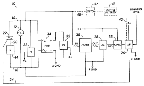
Particularly, refernng to Figure 5, the three wire dimmer switch 10 is
connected to the AC source 12 and to the lighting load 14 by wires 16, 18, 20,
in well
known fashion. The load 14 is in series with a control device 22 that controls
the RMS
voltage applied to the load 14 in accordance with control signals supplied to
a control
electrode 24 by the microprocessor 26. In the embodiments illustrated in
Figures 5, 6 and
7, the control device 22 is a controllably conductive device, such as a triac,
MOSFET,
IGBT, back to back SCR's, thyristors, etc., that receives trigger signals on a
gate electrode
24 thereof from the microprocessor 26. The microprocessor 26 receives an input
from a
zero crossing detector 28 via an optocoupler 35 and also receives data
indicative of the
selected dimming level. Zero crossing detector 28 provides an output signal to
the
microprocessor 26 each time that a zero crossing of the input signal thereto
is detected.
Microprocessor 26 is programmed in well known fashion to set the desired
dimming level
in response to the zero crossing indications and the selected dimming level. A
power
supply 32 supplies necessary DC power to the microprocesssor 26. A power
supply 33 on
the AC side of the bridge 34 supplies necessary power to the filter 30, the
zero cross
detector 28, and the optocoupler 35. A full wave bridge rectifier 34 is
employed to rectify
the AC line. The foregoing discussion is applicable to the three wire dimming
switch 10'
of Figure 6, but the explanation thereof is somewhat simpler. In Figure 6,
since the filter
30' is on the DC side of the bridge 34, the power supply 32 supplies necessary
DC power
to the filter 30, the zero cross detector 28, and the microprocessor 26 and a
separate supply
is not necessary. In Figure 5, the circuitry shown in dashed lines
(optocoupler 37 and the
"lightly filtered" circuit 41 ), and in Figure 6, the circuitry shown in
dashed lines (the
"lightly filtered" circuit 41), and their connections also shown in dashed
lines, are optional.
An explanation of the "lightly filtered" circuit follows hereinafter.
In the embodiment of Figure 7, the two wire dimming switch 10" is
connected to one side of the load and to one side of the AC line by wires 16,
18 in well
known fashion. Again, the load 14 is in series with a thyristor 22 that
controls the RMS
voltage applied to the load 14 in accordance with control signals supplied to
a control
electrode 24 associated with a control device 22 by the microprocessor 26. The
operation
CA 02305536 2000-03-31
WO 99/18651- PCT/US98/19842
-11-
of the two wire dimmer switch is otherwise essentially as set forth above.
Note optional
"lightly filtered" circuit 41, explained hereinafter.
In Figures 5, 6 and 7, information about the AC line 12 may be provided
over the optional connection 40 through the "lightly filtered" circuit 41 to
the
S microprocessor 26 for purposes described hereinafter.
According to the invention, the AC source voltage is provided to a low pass
active filter 30, 30' and the output of the filter 30, 30' is supplied to a
zero crossing detector
28. Thus, the AC line is filtered first, and the filter output is checked for
the occurrence of
zero crossings. The function of the filter 30, 30' is to substantially remove
or attenuate
frequency components of the AC line above the fundamental frequency (or above
twice
the fundamental frequency in certain cases), and to do so "quickly", i.e, with
minimum,
phase delay. In other words, the filter has a substantially flat frequency
gain characteristic
up to about the fundamental frequency (or up to about twice the fundamental
frequency in
certain cases) and a rapidly decreasing gain characteristic thereafter, and
interposes a
1 S substantially linear phase delay (constant time delay) in the pass band to
the fundamental
frequency component. The output of the filter therefore is the AC fundamental
component
(or the second harmonic frequency of the AC fundamental component in certain
cases),
time delayed by a constant amount relative to the AC line, that is
substantially free of
noise and distortion. Importantly, since the output of the filter is the AC
fundamental
component (or the second harmonic frequency of the AC fundamental component)
of the
AC line, any fundamental frequency variations on the AC line will appear in
the AC
fundamental component (or the second harmonic frequency of the AC fundamental
component) at the filter output. Therefore, the AC fundamental component (or
the second
harmonic frequency of the AC fundamental component) present at the filter
output is a
nearly ideal signal for zero crossing detection.
Figure l0A is a plot showing the AC line entering the filter 30, line 60 of
Figure 10A, and showing the output of the filter (AC fundamental), on line 62
of Figure
10A. Line 64 of Figure I OA shows the output of the zero crossing detector 28,
where
rising edges are indicative of zero crosses of the AC filndamental, line 62.
The plots
shown are for a SOHz line frequency, i.e., a lOmsec half period. The plot of
Figure l0A is
applicable to embodiments of the invention where the filter 30 is on the AC
side of the
dimming circuit, e.g., Figure 5. It will be seen that, in the example of
Figure 10A, the plot
CA 02305536 2000-03-31
WO 99/18651- PCT/US98/19842
-12-
62 of the output of the filter 30 is phase delayed relative to the AC line
plot 60 by
approximately Smsec. When the AC line 60 crosses from the negative half cycle
to the
positive half cycle (i.e., zero crosses) at point A, this is not detected by
the microprocessor
26 until point A' (approximately Smsec later). When the AC line 60 crosses
from the
positive half cycle to the negative half cycle at point B, this is not
detected by the
microprocessor until point B'. The total phase delay time is the filter delay
time. The
filter delay time is dependent on the cut off frequency selected. In the
preferred
embodiment, the cutoff frequency selected is SSHz. This results in
approximately a Smsec
filter delay time. The microprocessor 26 processes the information about the
zero crosses
from point B' to point C'; this is less than lmsec.
The information about the zero crosses is used by the microprocessor 26 to
determine the half period of the AC fundamental 62, which will be used in
order to
properly gate the thyristor. The microprocessor is programmed to attempt to
maintain
constant duty cycle. Constant duty cycle means that even if the AC line
frequency
1 S changes (which will change the time between zero crosses), the amount of
power output to
the load will be held constant. In order to maintain constant power while the
AC line
frequency is changing, the amount of time after the zero cross that the
thyristor is to be
fired must be adjusted. If the AC line frequency increases, e.g., if the
frequency changes
from SOHz to SO.lHz, the time between zero crosses decreases and the amount of
time
after the zero cross that the thyristor is to be fired must be decreased in
order to keep the
output power constant. The opposite happens when the frequency decreases.
Constant
duty cycle is explained in more detail below in relation to Figure 12.
Preferably, the filter 30 is designed to remove or substantially attenuate
frequency components of the AC line voltage waveform that are substantially
equal to
third harmonics and greater of the AC fiirldamental. Second order harmonics
are not an
issue on the AC line, and any noise and distortion components are likely to be
in a
frequency range greater than the second harmonic frequency. Though an ideal
filter would
provide no phase delay, practical filter implementations always interpose some
phase
delay. In the preferred embodiment of the filter 30 of the present invention,
the phase
delay should not be more than half the period of the fimdamental frequency
(i.e., less than
180°) to ensure proper dimming filnction. In a 60Hz line, conduction
angles of 135 ° or
more, which translates to about 1 - 3 msec of conduction time of the
thyristor, represents
CA 02305536 2000-03-31
WO 99/18651- PCT/US98/19842
-13-
the dimming range where noise, distortion, etc. are most likely to be
manifested as
flickering and intensity variations. Therefore, from a practical standpoint,
the phase delay
should be no greater than about 135 ° to provide adequate time (within
each half cycle of
the AC line) for the microprocessor to compute a conduction angle and fire the
thyristor
well within this range of the half cycle.
In the exarnplary plot of Figure 10A, if the requested dimming level is low
enough, it is still possible to fire the thyristor at point C', or after point
C' in the negative
half cycle, with the zero cross information of the same half cycle. It is at
these low light
levels when the present invention is most beneficial. If the requested dimming
level is
such that the thyristor must be fired at a point prior to point C' in a half
cycle, the system
will wait until the next half cycle and will use the information from the
previous half
cycle. The system will use the most recent zero cross and period information
available,
which may be from an earlier half cycle of the same polarity.
In a best case scenario, the microprocessor 26 will use information about
I 5 the zero cross from the same half cycle in which the thyristor is to be
fired. If the dimming
system is fading from a high light level to a low light level, the
microprocessor 26 will
change from using information a half cycle old (i.e., from the previous half
cycle) to using
information from the same half cycle to fire the thyristor. Determining and
programming
such a transition, however, may complicate the coding of the microprocessor.
For
simplicity, information about the length of the half cycle from two prior half
cycles may be
used. Another reason for waiting until the next positive half cycle to use
information
about the previous positive half cycle is that the positive half cycle and the
negative half
cycle might not be symmetrical about zero volts. It is preferred to correct
the dynamic
problems during the same polarity of half cycle that the problem occurred,
even if it is
delayed by a fizll cycle.
Turning now to Figure 5, it will be seen that the filter 30 is coupled to
receive the AC line 12 in unrectified form. In other words, as mentioned, the
filter 30 is
on the AC side of the circuit. The output of the filter 30 is supplied to zero
crossing
detector 28 as above described. Since the filter receives the AC line in
unrectified form,
i.e., the filter 30 receives the AC line at the fundamental frequency of 50/60
I-iz, the
criteria of an embodiment of the present invention may require that the gain
characteristic
CA 02305536 2000-03-31
WO 99/18651- PCTNS98/19842
-14-
of the filter be substantially flat up to about the fundamental frequency of
50/60 Hz, but
this is not critical to the overall operation of the invention.
In the dimmer switch 10' of Figure 6, the filter 30' (which is substantially
identical to filter 30, except as described hereafter) is coupled to receive
the output of the
S full wave bridge rectifier 34. Thus, in the embodiment of Figure 6, the
filter 30' is on the
DC side of the circuit, and receives the AC line in full wave rectified form
rather than in
unrectified form as in Figure S. The filter thus receives the AC line at twice
the frequency
of the AC line 12 (and at twice the frequency of the filter 30 of Figure 5).
Therefore, the
criteria of an embodiment of the present invention may require that the gain
characteristic
of the filter be substantially flat up to about the twice the fundamental
frequency of 50/60
Hz, i.e., that it be substantially flat up to about 100/120 Hz, although,
again, this is not
critical to the overall operation of the invention. The dimmer switch 10' of
Figure 6 is
otherwise identical to that of Figure 5.
Figure 1 OB is a plot showing the full wave rectified AC line 60' and the
recovered AC fundamental 62, i.e., the output of filter 30', for embodiments
of the
invention where the filter 30' is on the DC side of the dimming circuit, e.g.,
such as in the
embodiment of Figure 6. Note the phase delay between the two waveforms.
One important discovery that has been made in connection with the present
invention is that there is sufficient information in the full wave rectified
AC line to
essentially reconstruct the second harmonic frequency of the fundamental
component
therefrom. Thus, when a filter 30' is constructed as described herein and is
employed in
the dimmer switch 10' of Figure 6, the output of filter 30' will be the second
harmonic
frequency of the AC fundamental component, since the input is full wave
rectified. This is
illustrated in Figure lOB where the input full wave rectified AC line is
designated 60' and
the output of the filter 30' is labeled 62. It will be noted that the output
62 is phase delayed
in respect to the input 60', as discussed above.
The phase delay of output waveform 62 from input waveform 60' is due to
two components, a 90~ phase shift caused by the full wave rectification, i.e.,
2.Smsec for a
SOHz supply and a 3msec phase delay through filter 30', which has a corner
frequency of
I llHz, for a total phase delay of approximately S.Smsec.
In the dimmer switch 10" of Figure 7, the filter 30 is disposed across the
thyristor 22, and therefore receives the AC line in unrectified form, and the
preceding
CA 02305536 2006-O1-27
WO 99/1865 PCT/US98l19842
-15-
discussion of Figure S is therefore applicable. In a two wire phase control
dimmer switch,
such as shown in Figure 7, the voltage across the thyristor 22 is the only
available signal.
For each half cycle of AC line voltage, the voltage across the thyristor 22
begins at zero
and follows the incoming AC line. When the thyristor is gated on, the voltage
across the
thyristor 22 collapses to the forward voltage drop of the thyristor (typically
1.5 volts). The
voltage remains at the forward voltage drop until the end of the half cycle.
The signal
across the thyristor 22 is available for the control circuitry to interpret
and use far
controlling the thyristor 22, as well as ancillary circuitry. The signal
across the thyristor
22 always contains some component of fundamental line voltage. The signal also
contains
. a varying component of harmonics of the fundamental: This varying component
of
harmonics changes with light level setting as well as with incoming power line
quality. As
previously discussed, gating of a thyristor in an electronic dimmer requires a
steady zero
cross reference; this is also true for two wire dimmers. Since the zero cross
filter
previously described has the characteristic of finding the fundamental in
the.presence of
distorted waveforms, it is well suited for finding the fundamental remaining
in the voltage
across the thyristor 22'.
A four pole Bessel filter has been found to provide the desired results
discussed above. One preferred implementation of a four pole Bessel filter is
illustrated in
Figure 8A. The implementation of Figure 8A has particular application to the
embodiments of Figures 5, 6 and 7 since, as described below, its gain and
falloff
characteristics have been designed to meet the criteria discussed above in
connection with
Figure 6, namely a phase delay of no more than 135 ° at 120Hz.
(Implementation of a
similar filter to meet the criteria of Figures 5 and 7 is straightforward.)
THE ART OF
ELECTRONICS by Paul Horowitz and Winfield Hill, second edition ( 1991 ),
Chapter 5
(Active Filters and Oscillators), pp. 272-275, fully describes active filter
design and
design criteria, including design of Bessel filters, .
Figure 8B illustrates one embodiment of a zero crossing detector that may
be employed in connection with the present invention.
In Figures 8A and 8B, IC1 is a LM324N, as manufactured by SGS
Thomson.
CA 02305536 2000-03-31
WO 99/18651. PCT/US98/19842
-16-
Figure 9 illustrates the gain characteristic of the Bessel filter of Figure 8A
(curve 50) and also illustrates gain characteristics of a Butterworth filter
(curve 52 ) and a
Chebyshev filter (curve 54) designed to provide about 135 ° phase delay
at 120Hz, as may
be used with the embodiment of Figure 6. As will be seen, the Bessel filter of
Figure 8A
has a corner frequency of about 111 Hz and has (relative to the Butterworth
and
Chebyshev filters) a shallow gain rolloff such that the filter has no
appreciable gain (less
than 20%) above 300 Hz. In a similar filter designed for the embodiment of
Figure 5 or
Figure 7, the corner frequency would preferably be about 55 Hz and the rolloff
would be
such that the filter has no appreciable gain above about 150 Hz. Unexpectedly
and
advantageously, it has been found that a relatively shallow rolloff, such as
shown by curve
50 for the disclosed Bessel filter, provides the most frequency attenuation
with a constant
phase delay, and also provides the most frequency attenuation in the portion
of the
frequency spectrum of most importance, i.e., in the first few harmonics of the
fundamental.
A Bessel filter is preferred, but is not necessary, as the filter choice,
since a Bessel filter is
simpler to design and implement, and because it has a relatively constant
phase delay,
regardless of the AC line frequency.
Referring to Figures l0A and IOB, it will be seen that the filter output
(recovered AC fundamental on line 62), or second harmonic frequency of the AC
fundamental on line 62') is substantially cleaner than the incoming AC line.
Figures 11A and 11B are spectral plots of an exemplary AC line into, and
the recovered signal out of, the filter 30, respectively. It will be seen that
the frequency
content of the recovered signal above the fimdamental frequency is
substantially reduced
relative to that of the AC line.
Figure 12 is a self explanatory flow diagram for the microprocessor 26 for
maintaining constant duty cycle. In order to make optimum use of the stable
zero cross
information, it is important to keep the thyristor conduction time a fixed
duty cycle of the
fimdamental AC line frequency. in order to accomplish this, the computations
to find the
thyristor turn on point must first use the latest period time to find the high
end and low end
limits. At 200, the microprocessor captures the most recent zero cross (TB)
and the
previous zero cross (TA) of the output of the filter 30, 30' and then
calculates the half cycle
period. In a system presently commercially available from the assignee of the
present
application, sold under the name Grafik Eye 4000 Series Dimming Panels, the
end user is
CA 02305536 2000-03-31
WO 99/1865I~ PCT/US98/19842
-17-
allowed to set the maximum high end and the minimum low end. By adjusting the
high
end, the end user can either reduce the maximum voltage and extend
incandescent bulb life
or increase the maximum voltage and obtain more light output. At 202, the
microprocessor calculates the high end as a fiznction of the period. By
adjusting the low
end, the end user can properly set the minimum voltage which is very important
with
fluorescent loads. At 204, the microprocessor calculates the low end as a
function of the
period. The high end adjustment range is 50% to 95% (K), with the setting
typically at
about 95% for incandescent loads and at about 70% for fluorescent loads. For
the typical
incandescent load, set at the high end on a 60Hz line, this results in a
firing time of
approximately 0.42msec after the zero cross of the AC line. The low end
adjustment range
is 5% to 49% (M), with the setting typically at about 5% for incandescent
loads and at
about 30% for fluorescent loads. For the typical incandescent load set at the
low end on a
60Hz line, this results in a firing time of approximately 7.92msec after the
zero cross of the
AC line. The system allows the end user to set a dimmer to a light level by
selecting a
value from a digital display. The display has an intensity range of 0-100,
where an
intensity I = 100% represents the high end and an intensity I = 0% represents
the low end.
At 206, the microprocessor determines the amount of time after the zero cross
of the AC
line to fire the thyristor using the formula: Fire = High end + (low end -high
end) * (1-I).
At 208, the microprocessor then fires the thyristor at time TB - phase delay +
Fire using a
phase delay value retrieved from memory at 207. This phase delay value is the
phase
delay, ~ delay, shown in Figures l0A and l OB. A nominal value for the phase
delay of an
ideal filter, e.g., Smsec, can be stored in microprocessor 26 when the system
is
manufactured. This nominal value can be replaced with a value which reflects
the
measured actual phase delay of the specific filter 30, 30' connected to the
microprocessor
26 as described below in connection with Figure 13. At 210, the microprocessor
then
waits for the next zero cross, and the sequence begins again at 200.
It has been determined that, in mass production, the amount of phase delay
through filters 30, 30' of Figures 5, 6 and 7 will vary by as much as 200
microsec within
the same lot of components due to component tolerance. A variation of this
size can cause
undesired results especially at low light levels where the on time of the
thyristor may be as
little as 900 microsec. The phase delay may also change slowly as the
components age or
as the operating temperature changes. In order to compensate for this
variation, the
CA 02305536 2000-03-31
WO 99/18651 PCT/US98/19842
-18-
microprocessor 26 may be programmed to adjust for changes in the phase delay.
Figures
5, 6 and 7 show, in part, a "lightly filtered" AC line input into the
microprocessor 26. This
circuit detects zero crosses directly off the AC line or through optional
optocoupler 37 in
the circuit of Figure 5, with little or no phase delay. "Light filtering" can
be performed by
a simple (usually passive) low-pass filter, for example a single resistor-
capacitor stage,
whose cutoff frequency is low enough to remove as much as possible of the line
noise, but,
high enough that the phase delay it introduces at the fiuldamental frequency
is small
enough that variation of that phase delay with variation with component
tolerances (even
with low-precision components) is insignificant. Alternatively, the light
filtering can be
performed by software routines incorporated into microprocessor 26. Figure 13
shows a
filter phase delay compensation flowchart. In this embodiment of the
invention, the
system monitors the lightly filtered AC line 42 and measures the phase delay
between it
and the "heavily filtered" AC fizndamental or second harmonic frequency of the
AC
fimdamental output from the filter 30, 30'. "Heavy filtering" can be performed
by a low-
pass filter (such as the active low pass filter described above) whose cutoff
frequency is
close to the fundamental line frequency (or twice that frequency, when the
input to the
filter is a full-wave rectified waveform), or a narrow-band pass filter.
Using this information, the microprocessor 26 can derive the phase delay of
the actual filter 30, 30' from the difference between the heavily filtered and
lightly filtered
inputs. Even if the lightly filtered line 42 is unstable due to line noise,
the microprocessor
26 can average this value over many line cycles to minimize the influence of
the noise.
Thus, the microprocessor 26 can compensate for the phase delay.
Figure 13 shows a flow chart for implementing the zero cross filter delay
compensation system shown in dashed lines in Figures 5, 6 and 7. At 100, the
microprocessor captures a zero cross from the lightly filtered line 42 into
the
microprocessor 26 as T1. At 102, the microprocessor captures a zero cross from
the
heavily filtered line output from the filter 30, 30' into the microprocessor
26 as T2. At
104, the microprocessor calculates the difference between T1 and T2 and stores
it as OTn.
At 106, the microprocessor takes an average of the last K samples of OTn and
stores this
as OTavg, where K is an empirically chosen value from 10 to 10,000. At 108,
the
microprocessor stores 0 Tavg as the phase delay value to be retrieved at step
207 of the
routine illustrated in Figure 12 in place of any previously stored value.
CA 02305536 2006-O1-27
WO 99/18651- PCTNS98/198a2
-19-
The routine illustrated in the flow chart of Figure 13 is performed
periodicahy to update the stored value of the phase delay. It is typically
done whenever
power is applied to the system and then at least once per day. However, it can
be
performed as frequently as many times per second.
Those skilled in the art will appreciate that a band pass filter, a circuit
containing passive circuit elements, a switched. capacitor filter or a
software
implementation of the analog hardware filter (i.e. a sofhvare filter)
disclosed lierein may be employed. and sncli
substitution is within the scope of the present invention. A system employing
digital
signal processior (DSP) with a high speed analog to digital converter (i.e.,
greater than 20
kHz) can sample and then recreate the incoming AC line. Using either a fast
Fourier
transform or DSP programmed to perform as a low pass or band pass filter, the
system can
"filter" out any frequency above the fundamental. This could be used instead
of the filter
described above. The remaining fi.tndamental frequency can then be fed into
the zero cross
detector and then into the microprocessor in order to properly fire the
thyristor, as was
previously described. The DSP, zero cross detector and microprocessor can be
incorporated into one device.
The present invention may be embodied in on other specific forms without
departing from the spirit or essential attributes thereof, and accordingly,
reference should
be made to the appended claims, rather than to the foregoing specification, as
indicating
the scope of the invention.