Note: Descriptions are shown in the official language in which they were submitted.
CA 02305571 2000-03-31
WO 99/16941 PCT/US98/20407
- 1 -
SUBSTRATES FOR SUPERCONDUCTORS
This invention was made under a Cooperative
Research and Development Agreement with Los Alamos
National Research Laboratory. The United States
Government has certain rights in this invention.
Background of the Invention
The present invention relates to substrates for
superconductors, and more particularly to copper-nickel
substrates for receiving the deposition of YBCO
(YBa2Cu30X, or Yttrium-Barium-Copper-Oxide) high
temperature superconducting layers to form so-called YBCO
coated conductors. Other closely related superconducting
materials which can be used are REBa2Cu30x, in which the Y
has been partially or completely replaced by rare earth
(RE) elements.
YBCO (Y-Ba2-Cu3-OX) is an important superconducting
material for the development of superconducting tapes
that can be used in superconducting transmission cables,
superconducting current leads, superconducting coils for
transformers, superconducting magnets for AC and DC motor
applications, and superconducting current limiters, as
well as other electrical conductors. These applications
are based on a basic property of a superconducting
material: it has no electrical resistance when cooled
below its transition temperature, and can carry a DC
electric current without power dissipation.
CA 02305571 2000-03-31
WO 99/16941 PCT/US98/20407
- 2 -
For the production of YBCO coated conductors, thin
substrate tapes (or foils) are typically coated with a
thin buffer layer, which in turn is coated with a YBCO
layer. A suitable heat treatment is then performed to
optimize the superconducting properties of the YBCO
layer. One of the functions of the substrate is to
impart mechanical strength to the resulting
superconducting tape. A second function, which depends
on the process type, is to act as a template for a well-
textured buffer layer. Compared to the substrate
material, this buffer layer provides a much better
deposition surface for the YBCO layer in terms of lattice
match, texture, coefficient of thermal expansion (CTE)
and chemical compatibility. To obtain good
superconducting properties, the buffer layer needs to be
bi-axially textured - meaning that a lattice plane,
preferably its cubic (or tetragonal) lattice face, is
oriented such that the cube face is parallel to the tape
surface in a substantial majority of its crystallites.
In addition, the cube edge in each crystallite should be
parallel to the cube edges in all neighboring
crystallites.
Some specialized techniques such as Ion Beam
Assisted Deposition (IBAD) or Inclined Substrate
Deposition (ISD) can deposit a bi-axially textured buffer
layer on top of a random polycrystalline or even
amorphous substrate. In general, these deposition
CA 02305571 2000-03-31
WO 99/16941 PCT/US98/20407
- 3 -
techniques are very slow or are effective in only a
narrow region, and they are not suited for large scale
and economical manufacturing of YBCO coated conductors.
A more advantageous method is the epitaxial deposition of
a bi-axially textured buffer layer (or YBCO
superconducting layer) on top of a bi-axially textured
metallic substrate. Examples of epitaxial growth by
vapor deposition, electro-plating, or oxidation, in which
native oxide layers grow on parent metals, are numerous
and well known, as is the fact that many metals can form
bi-axial textures. Few of these textures are useful for
deposition of buffer layers and YBCO superconducting
layers because of misorientation. However, in many
rolled, face-centered cubic (fcc) metals, when properly
rolled and heat treated, a well-developed, and very
useful, cube texture is obtained. The cube faces are
parallel to the rolled surface and a cube edge typically
points in the same direction as the rolling direction.
Such a texture is called a cube-on-cube texture, with a
crystallographic notation of (100)[001]. Another well-
known cube texture is the so-called Goss texture
(100)[011]. These bi-axial textures are part of a larger
family called sheet textures. In the following
description of the invention the (100)[001] texture will
be referred to as the "cube" texture.
To deposit the buffer layer in an epitaxial manner
on the substrate, the substrate material needs to meet
CA 02305571 2000-03-31
WO 99116941 PCT/US98/20407
- 4 -
certain requirements. The substrate must have a lattice
constant and a CTE which are compatible with the buffer
layer material and also with the YBCO layer. Ideally,
the substrate will yield a bi-axial texture by simple
thermo-mechanical means. The substrate is preferably
non-magnetic at cryogenic temperatures, that is, at
temperatures between room temperature and that of liquid
helium, or 4.2 degrees Kelvin. The substrate must be
electrically conductive, relatively strong at room
temperature, and oxidation resistant at elevated
temperatures. There are several metals, such as copper
or nickel, that can be bi-axially textured by rolling a
selected copper or nickel stock, followed by a so-called
secondary recrystallization at an elevated temperature.
However, these pure metals have significant drawbacks in
that they are either ferromagnetic (Ni) or are easy to
oxidize (Cu).
It is known that some binary alloys (a single
phase mixture of two metals) can be made into a bi-
axially textured tape as well. One example of a cube
texture which has been produced in an alloy is iron-
nickel, but this alloy has proven to be ferromagnetic,
which is detrimental to the performance of the device in
many applications. In addition, copper-nickel alloys
with small quantities of nickel have previously been
textured, but those working in the field believed that
CA 02305571 2000-03-31
WO 99/16941 PCT/US98/20407
- 5 -
the maximum Ni content in the Cu-Ni alloy should not
exceed 4.2 percent nickel.
Summary of the Invention
The present invention features bi-axially textured
alloys with a face centered cubic structure, of copper-
nickel (Cu-Ni) with 5 to 45 atomic % nickel, preferably
10-40% and more preferably 25-35%, for use as substrate
materials for superconducting oxides. Preferred
superconducting oxides include the Rare Earth Barium
Copper Oxides, {RE)BCO, or Yttrium Barium Copper Oxides,
YBCO, but also superconducting oxides from the Thallium,
Mercury and Bismuth families. The combination of the
substrate and the oxide forms a coated conductor. These
Cu-Ni alloys are preferably homogenous, but can have some
degree of inhomogeneity with localized concentrations of
Ni not exceeding 45%, and can be processed by thermo-
mechanical methods to form tapes with a single {100)[001]
cube texture. These alloys are non-ferromagnetic and
form good substrate materials for subsequent epitaxial
buffer layer and superconductor layer deposition, for use
in a variety of products.
The enhanced Ni content achieves desirable
features in the alloy, such as increased oxidation
resistance, decreased CTE, and increased room temperature
and high temperature strength. The increased Ni content
does not cause ferromagnetism as long as the Ni content
does not exceed 42% for applications down to 4.2 degrees
CA 02305571 2000-03-31
WO 99/16941 pCT/US98/20407
- 6 -
Kelvin or 45% for applications at temperatures between
4.2 and 77 degrees Kelvin. With the appropriate buffer
layer material, this substrate will not adversely affect
the superconducting properties of the superconducting
layer.
Cube-textured alloys of the present invention are
formed by creating a homogenous solid solution of the
alloying elements. The Cu and Ni constituents are
weighed, mixed, and melted together to form a CuNi alloy.
The starting materials are preferably at least 99% pure.
The melt is then cooled to room temperature. The rate of
cooling can be slow or fast, with a rapid quench
preferred for giving a fine grain size. The solidified
alloy is further homogenized by a heat treatment. The
alloy is then processed into tape by mechanical means,
such as rolling, after which a suitable heat treatment
produces the desired cube texture. An optional
recrystallization step after the homogenization and
partial deformation of the alloy induces a refined grain
size' of 5 to 70 micrometers, which obtains a cube texture
in the rolled and heat treated tapes.
Brief Description of the DrawincLs
Fig. 1 is a block diagram illustrating the process
of forming a cube-textured alloy substrate.
Fig. 2 illustrates a partial cross-sectional view
of a superconductor composite formed with a cube-textured
alloy substrate.
CA 02305571 2000-03-31
WO 99/16941 PCT/US98/20407
Fig. 3 illustrates a partial cross-sectional view
of a superconductor composite formed with a cube-textured
alloy substrate and a textured buffer layer.
Figs. 3A and 3B illustrate partial cross-sectional
views of superconductor composites formed with multiple
buffer layers.
Fig. 4 illustrates a partial cross-sectional view
of a superconductor composite having both sides coated
with a buffer layer and a superconducting layer.
Fig. 5 illustrates a cross-sectional view of a
superconductor composite in which the coated layers
surround the substrate.
Fig. 6 illustrates a cross-sectional view of a
superconductor composite with multiple buffer and
superconducting layers:
Figs. 7-10 are pole figures of cube-textured
alloys.
Description of the Embodiments
The present invention provides an alloy with a
cube texture which is formed from a single phase mixture
of 5 to 45 atomic percent nickel with the balance being
copper. A method for making the alloy is also featured.
The cube texture is often indicated by the
crystallographic notation (100) [001] and is typically
formed by sheet or tape rolling of a suitable metal or
alloy, followed by an appropriate heat treatment. Metals
or alloys with a face centered cubic (fcc) structure, and
CA 02305571 2000-03-31
WO 99/16941 PCT/US98/20407
g _
which have been processed to display a bi-axial cube
texture, have crystallites in which the cube faces are
parallel to a tape surface while the cube edges point in
the rolling direction. The cube-textured alloys of the
present invention are particularly useful as substrate
materials for superconducting composites. The resulting
tape-like structure includes a cube-textured substrate,
on which, for example, a bi-axially textured buffer layer
can be deposited using an epitaxial deposition process.
Subsequently, a bi-axially textured superconducting layer
can be deposited, again using an epitaxial deposition
process.
The quality of the bi-axial cube texture
determines the effectiveness of the substrate for use in
super-conducting composites. The orientation of the cube
oriented grains should be within a few degrees of the
ideal bi-axial cubic orientation. Grains with an
orientation which deviates from the cube texture, should
be small in number, preferably well below 15 volt. The
quality of these textures is revealed in their X-ray
diffraction pole figures, which show the collective
orientations of all crystallites in the irradiated area.
Random orientations show no concentration in any
direction. Quality textures, on the other hand, show
sharp peaks in the pole figures. The sharpness of these
peaks is expressed as the Full Width Half Maximum (FWHM)
value and is indicative of texture quality. The lower
CA 02305571 2000-03-31
WO 99/16941 PCT/US98/20407
_ g -
the FWHM value, the sharper the peak, and hence, the
better the texture. For polycrystalline materials, a FWHM
value of well below 10° is desired. Typically, FWHM
values on the order of 4-15° are achieved in the
substrates of this invention. Higher FWHM values can be
acceptable for substrate purposes, in particular if this
reduced texture is off-set by advantages in other areas,
such as improved oxidation resistance, or better chemical
or CTE compatibility. In general, alloy substrates result
in FWHM values that are often slightly higher than the
FWHM values of similarly treated pure metal constituents.
The alloying does, however, lead to advantages as
mentioned above, such as a non-magnetic substrate,
improved oxidation resistance, and improved CTE.
When these substrates are used to form super-
conducting composites, a buffer layer and superconducting
layer can be on one side, both sides, partially, or
entirely surround the substrate conductor. The buffer
layer can be a metal layer or oxide layer, or
combinations of both. Each must provide the needed
texture, chemical compatibility, matching lattice
constant, and proper CTE match. For example, the buffer
layer can be a noble metal or noble metal alloy, an oxide
with a cubic structure such as, but not limited to, MgO,
Ce02, Yb203, or yttria-stabilized zirconia ("YSZ"), or any
combination of oxides and/or noble metals. The buffer
layer, which can include multiple layers, is preferably
CA 02305571 2000-03-31
WO 99/16941 PCT/US98/20407
- 10 -
deposited in an epitaxial manner, in which the bi-axial
texture of the substrate is transferred onto the buffer
layer, or first layer of the buffer layer if multiple
buffer layers are employed. In this latter instance,
each buffer layer transfers its texture to the next layer
until the buffer layer is completed. Finally, the top
buffer layer transfers its texture onto the YBCO
superconducting layer.
Cube-textured alloys of the present invention are
formed by creating a homogenous solid solution of the
alloying elements. The Cu and Ni constituents are
weighed, mixed, and melted together to form a CuNi alloy.
The starting materials are preferably at least 99% pure.
The melt is then cooled to room temperature. The rate of
cooling can be slow or fast, with a rapid quench
preferred for giving a fine grain size. The solidified
alloy is further homogenized by a heat treatment. The
alloy is then processed into tape by mechanical means,
such as rolling, after which a suitable heat treatment
produces the desired cube texture. An optional
recrystallization step after the homogenization and
partial deformation of the alloy induces a refined grain
size of 5 to 70 micrometers, which obtains a cube texture
in the rolled and heat treated tapes.
The binary alloys of the present invention have 5
to 45 atomic percent nickel, preferably 25 to 35%, with
the balance being copper. The upper limit of 45 atomic
CA 02305571 2000-03-31
WO 99/16941 PCT/US98/20407
- 11 -
percent nickel is established to minimize the risk of
developing ferromagnetic properties, which are
detrimental to the performance of the device in many
applications of the oxide layer. Further, by remaining
below the upper limit, the strong bi-axial cube texture
of the alloy is maintained, and the alignment of lattice
edges allows the alloy to act as a substrate for
superconducting applications.
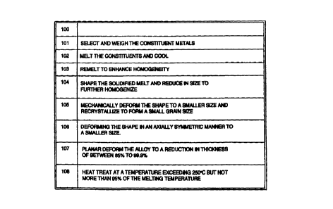
Referring to Fig. 1, a block diagram illustrates
the process 100 for forming a cube-textured alloy. The
cube-textured binary alloys of the present invention are
created by first selecting and weighing the constituent
metals (Step 101) in a mixture of 5 to 45 atomic percent
nickel, preferably 10-40% and more preferably 25 to 35~,
with the balance being copper. This solid solution is
then melted (Step 102) by various processes known in the
art, such as arc melting, induction melting, plasma torch
melting, or melting in an electrical resistance furnace
or a furnace heated by gas or coal. Melting temperatures
range from 1100°C to 1250°C. A certain level of
homogenization is achieved during the melt process due to
convection, mechanical stirring, or stirring induced by
the melting techniques such as the induction melter. The
melting can be performed in air, under vacuum, or under a
protective inert atmosphere such as nitrogen, argon or
helium etc. The melting can be repeated several times to
further increase homogenization (Step 103). The melt is
CA 02305571 2000-03-31
WO 99/16941 PCT/US98/20407
- 12 -
then cooled with the furnace. The solidified melt is
shaped, preferably, into a bar. The bar is reduced in
diameter by rod rolling, swaging, drawing or extrusion by
a factor of about 1.3 to about 20, preferably about 1.3
to 5, and heat treated to further homogenize the alloy
(Step 104). A further mechanical reduction in diameter by
similar mechanical means follows, to a size where the
planar deformation process will commence (Step 105).
Before or at this stage a heat treatment can be applied
to recrystallize the alloy and obtain a fine grain size
of approximately 5 to 70 micrometers, preferably greater
than 10 micrometers and less than 40 micrometers (also
Step 105). Alternatively, other methods can be utilized
to achieve a fine grain size, such as the rapid
solidification of the alloy after melting. An example is
the atomization of a melt into an alloy powder, which is
subsequently consolidated by (hot) pressing or extrusion
into a bar, and which is processed subsequently similar
to a cast alloy. The alloy sample is subsequently
deformed in an axially symmetric manner, such as
extrusion, swaging, drawing, or rod rolling to a smaller
size which can be round, square or rectangular (Step
106). In yet another alternate process step, the melt can
be cast and rolled. This cast can be further homogenized
with a suitable heat treatment, rolled to a thinner size,
and recrystallized to induce a fine grain size.
CA 02305571 2000-03-31
WO 99/16941 PCT/US9$/20407
- 13
The alloy is then deformed further by various
planar rolling methods known in the art (Step 107), to
reduce the thickness of the stock by at least 85% and up
to 99.9%. The planar deformation is performed at
temperatures between -200 and 600°C, and preferably at
room temperature. A recrystallization anneal (Step 108)
at a temperature exceeding 250°C, but not more than 95% of
the melting temperature, and preferably at temperatures
between 400 and 1190°C, produces the desired single cube
texture (100)[001]. Fig. 7 shows a (111) pole figure, of
a Cu-16 at% Ni alloy, which demonstrates a single and
high quality (100)[001] cube texture. This alloy is made
by extrusion of the homogenized alloy to tape, rolling
the tape to a reduction in thickness of 96%, and heat
treating the final tape at 850°C for 4 hours in a
protective atmosphere. (See Example 3).
Rolling processes suitable for use with the
present invention utilize the following parameters.
Rolling is typically performed at room temperature, with
rolling between O.lOm/minute and 100m/minute. The
reduction schedule can be a constant reduction per pass,
or a constant strain per pass, with reduction steps
chosen to be between 5 and 40% per pass. The tape can
be lubricated during rolling, or rolled without any
lubricant. Bidirectional rolling is preferred. The
tapes can be rolled with large diameter rolls (3.5" to 8"
or larger in diameter) or preferably with small diameter
CA 02305571 2000-03-31
WO 99/16941 PCT/US98/20407
- 14 -
rolls (0.75" to 2" in diameter) which can be backed up by
larger rolls, in a so-called four-high arrangement.
Alternatives to the four-high arrangement are cluster and
planetary rolling mills.
Referring to Fig. 2, a partial cross section of a
superconducting composite 200 is shown. To form a
superconducting composite 200, the above described
substrates 201 of cube-textured alloys have at least one
surface 202 coated with a superconducting oxide 203, such
as yttrium-barium-copper-oxide (YBCO) or a rare earth
barium copper oxide (REBCO) or mixtures of these. The
REBCO's are formed by partial or complete substitution of
yttrium (Y) in the YBCO with rare earth elements such as
praesodium, neodymium, samarium, europium, gadolinium,
terbium, dysprosium, holmium, erbium, thulium, ytterbium,
lutetium, lanthenum, or cerium. The coating of the
superconducting oxide 203 is preferably approximately 0.2
to 20 micrometers thick, more preferably 1-20 micrometers
thick. The coating is applied by any deposition
technique, such as a non-vacuum solution deposition,
electroplating, chemical vapor deposition, or physical
vapor deposition techniques, such as sputtering, laser
ablation, thermal evaporation, electron beam evaporation.
These deposition techniques can require a heat treatment,
such as that disclosed in U.S. Patent No. 5,231,074
issued to Cima et al., fully incorporated herein by
CA 02305571 2000-03-31
WO 99/16941 PCT/US98/20407
- 15 -
reference, to form the YBCO in an epitaxial manner, and
optimize its superconducting properties.
In the Cima patent, highly-textured superconductor
oxide thin films are prepared on substrates, including
lattice matched, non-lattice matched, inert and non-inert
materials, by metal organic deposition (MOD). Precursor
solution composition, as well as processing temperature
and atmosphere are selected to control the presence of a
transient liquid phase. Superconductor oxide films
characterized by highly textured morphologies and fully
dense, homogeneous microstructures are capable of
sustaining critical current densities in excess of 104
A/cmz at 77 degrees K. when prepared on non-lattice
matched substrates or critical current densities in
excess of 106 A/cm2 at 77 degrees K. when prepared on
lattice-matched substrates.
Referring now to Fig. 3, in order to improve the
surface characteristics of the substrate 301 of composite
300, for receiving a superconducting oxide coating 303, a
buffer layer (or multiple buffer layers) 302 is deposited
in an epitaxial process onto the cube-textured alloy
substrate 301. Any of the deposition processes listed
above, among others, can be used for depositing the
buffer layer 302. A heat treatment can be included to
form the buffer layer in an epitaxial manner. The buffer
layer 302 has a thickness of approximately 0.1 to 10.0
micrometers, and preferably 0.1 to 5.0 micrometers more
CA 02305571 2000-03-31
WO 99/16941 PCT/US98/20407
- 16 -
preferably 0.2 to 0.8 micrometers. It includes a single
metal or oxide layer, or can be a multiple layered
structure. A structure in which the buffer layer has two
layers is shown in Fig. 3A where the substrate 301 is
covered with a layer 304 and subsequently a second layer
305, where the combination of layers 304 and 305 form the
buffer Layer. The multiple layers 304 and 305 can
include any combination of layers, such as a metal layer
304 with an oxide layer 305 on top, or an oxide layer 304
with another oxide layer 305 on top. Alternatively,
referring to Fig. 3B, the buffer layer can include three
or even more layers. In this arrangement, the substrate
301 is coated with a metal or oxide layer 306 which in
turn is coated with additional metal or oxide layers 307
and 308 before deposition of the superconducting layer
3 03 .
Referring to Figs. 3, 3A and 3B, a top layer 310
comprising a noble metal (such as silver, gold,
palladium, platinum, rhodium, iridium, rhenium or alloys
thereof) is optionally deposited on the superconducting
layer 303. This layer 310 prevents environmental
degradation of the superconducting layer, and provides an
alternative current path if the superconducting layer is
locally degraded and unable to fully carry the
superconducting current. Also, layer 310 provides an
additional site to solder the conductor.
CA 02305571 2000-03-31
WO 99/16941 PCTNS98/20407
- 17 -
The metals for the top and buffer layers are
typically noble metals or noble metal alloys. By ~~noble
metal~~ is meant a metal whose reaction products are
thermodynamically stable under the reaction conditions
employed relative to the desired superconducting ceramic,
and/or a metal which does not react with the
superconducting ceramic or its precursors under the
conditions of manufacture of the composite. The noble
metal can be a metal different from metallic matrix
elements of the desired superconducting ceramic. The
noble metal can be silver or a silver/gold alloy, but it
can also be a stoichiometric excess of one of the
metallic elements of the desired superconducting ceramic,
such as yttrium. Silver (Ag) and silver alloys are the
most preferred noble metals. Other noble metals include
platinum, gold, palladium, rhodium, iridium, ruthenium,
rhenium or alloys thereof. The oxides that are used for
the buffer layers are typically stable oxides with a
cubic structure such as MgO, cubic A1203, yttria, YSZ, or
rare earth oxides such as Ce02, Yb203 etc. or mixtures of
these oxides.
By coating the entire substrate, front, back,
and/or the sides, with a buffer layer before the
deposition of the auperconducting layer, the oxidation
resistance of the substrate is improved. Fig. 3 shows a
substrate with this optional buffer layer 309 on the
bottom side of the substrate.
CA 02305571 2000-03-31
WO 99/16941 PCT/US98/20407
- 18 -
Referring to Fig. 4, there is shown a partial
cross-section of a superconducting composite 400. In
this embodiment, the composite 400 has a substrate 401
with a pair of surfaces that are each coated with a
buffer layer 402. A superconducting oxide 403 is coated
on each of the buffer layers 402. In an alternate
arrangement, as shown in Fig. 5, the composite 500 has a
substrate 501 which is fully surrounded by a buffer layer
502. Furthermore, a superconducting oxide layer 503
fully coats the buffer layers 502 on all surfaces of the
composite 500.
Referring to Fig. 6, there is shown a partial
cross section of a superconducting composite 600. In
this embodiment, the composite 600 has a substrate 601.
with a pair of surfaces that are each coated with a
buffer layer 602. A superconducting oxide 606 is then
coated on one side of buffer layer 602. A second buffer
layer 603 is coated onto layer'606, after which a second
superconducting oxide layer 607 is deposited on this
2o buffer layer 603. In this manner, a multi-layered
structure can be built which, for example, has four
superconducting layers (606, 607, 608 and 609)
interspersed with three substrate layers (603, 604, and
605). This multiple structure increases the current
carrying capability of the conductor. In this example,
the top superconducting layer 609 is coated with a noble
metal layer 610 for environmental protection of the
CA 02305571 2000-03-31
WO 99/16941 PCT/US98/20407
- 19 -
superconductor 609, an alternate current path, and
additional sites to solder the conductor.
EXAMPLE 1
A cube-textured copper-nickel alloy according to
the present invention is produced according to the
following method. 99.999 pure Ni and Cu pieces (pellets
mixed with coarse powders) are weighed in a ratio of 68
ate Cu and 32 ate Ni. The pieces are mixed and loaded in
a water cooled copper hearth of an arc melter which
i0 operates in a protective atmosphere. The Cu+Ni mixture
is melted and solidified several times, to ensure
adequate mixing, at a temperature well above the melting
temperatures for several minutes. The solidified and
cooled alloy is mechanically formed in the shape of a
solid cylinder, and is rolled, using 10~ deformation per
pass, to a total reduction of 99~ without any
intermediate stress anneal process. The resulting tape
is heat treated at 850°C for 4 hrs using a protective gas
of 95% argon and 5~ hydrogen. This tape shows mainly a
single, bi-axial cube texture, with a minor twinning
element which can be seen in the (111) pole figure of
Fig. 8.
EXAMPLE 2
A 32 mm diameter oxygen free copper can is loaded
with a mixture of Cu and Ni pieces, and the overall exact
CA 02305571 2000-03-31
WO 99/16941 PCT/US98/20407
- 20 -
stoichiometry (including the weight of the copper can) is
further adjusted with Cu powder, to a mixture of 16 at%
Ni, 84 at% Cu. This can is placed inside a 38 mm
diameter thin-walled alumina crucible and heated in a
protective atmosphere using a induction melter at about
1170°C, for up to 5 minutes. The use of the induction
melter and the fact that the alumina is not an electrical
conductor causes stirring in the melt, which promotes
homogenization. After solidification, the alloy is
removed from the crucible. To enhance homogeneity, the
cast is remelted using a similar crucible and the same
induction melter, again under vacuum and at the same
conditions. The cast alloy, which has a cylindrical
shape, is machined to a diameter of 31 mm and extruded to
a 17 mm diameter bar. This bar is homogenized at 950°C
for 24 hrs. It is machined to a 16 mm diameter billet,
suitable for hydrostatic extrusion. It is extruded to a
3 mm diameter wire and subsequently rolled using a
reversible direction rolling technique, with a four-high
rolling mill at a rolling speed of 6 m/min, and reduction
per pass of 10%. The total reduction in thickness is
98.9%. Subsequently, it is heat treated at 850°C for 4
hrs under a 95% argon - 5% hydrogen gas mixture. This
tape has a single bi-axial cube texture and a FWHM value
of 6°. A (111) pole figure is shown of this alloy in
Fig. 7. The pole figure demonstrates a single, high
quality cube texture.
CA 02305571 2000-03-31
WO 99/16941 PCT/US98/20407
- 21
EXAMPLE 3
A similar process is followed as in Example 2, but
the mixture is 26.5 at% Ni and 73.5 at % Cu. The alloy
was extruded to a tape, which was rolled to a reduction
in thickness of 96%. The tape was heat treated for 4
hours at 850 degrees Celsius. The final tape made with
this alloy has a single bi-axial cube texture, with a
FWHM value of 12°. A (111) pole figure of this alloy is
shown in Fig. 9.
EXAMPLE 4
A similar process is followed as in Example 2, but
now the mixture is 37 at% Ni and 63 at % Cu. The final
foil made with this alloy again has a single bi-axial
(100)[001] cube texture, with a FWHM value of 10°. A
(111) pole figure of this alloy is shown in Fig. 10.
It will be obvious to those skilled in the art
that various changes and modifications can be made
therein without departing from the scope of the invention
as defined by the appended claims.