Note: Descriptions are shown in the official language in which they were submitted.
CA 02305706 2000-OS-04
WAVEFORM SHAPING METHOD AND EQUIPMENT
This application is a divisional of Patent Application
No. 2,126,598 filed June 23, 1994.
BACKGROUND OF THE INVENTION
Field of the Invention
The present invention relates to the waveform shaping
equipment and waveform-shaping method for generating
bandlimited signals, and for preventing band spread at the
head and trail at the edge of burst when burst-like data
string is transmitted in the data transmission in which data
is transmitted in the form of packet.
Related Art of the Invention
In the radio communication, etc., when a packet comprising
transmission data is transmitted, it is necessary to limit the
bandwidth (bandlimitation) to prevent adjacent channel
interference for effective utilization of frequency. For
bandlimitation of signals, it is common to limit the bandwidth
with respect to the signal waveform of the baseband. Two
systems are available for band-limiting the baseband signal
waveform: an analog system using analog filter and a digital
system by digital signal processing. One of the digital
systems is the method to shape waveform by reading out and
concatenating the baseband signal waveform previously band-
limited by calculation from the memory table such as ROM and
the like (for example, IEEE Transactions on Communications,
COM-Volume 25, No. 10, Pages 1243-1244). When the waveform
shaping method using this memory table system is used, the
ideal filter frequency
1
CA 02305706 2000-OS-04
response can be more accurately realized than the analog
system waveform shaping method, and the shaped waveform can
be changed only by rewriting the memory contents, achieving
high versatility. It is also suited for the VLSI technique
and can be comparatively downsized.
Referring now to the drawings, the conventional
waveform shaping equipment using the above-mentioned method
is described with special emphasis placed on the readout
principle of shaped waveform and hardware configuration of
the waveform shaping equipment.
FIG. 1 shows input data to the waveform shaping
equipment. D(1), D(2), ....., D(k), ..... D(n) show
transmission data and X shows the data other than the
transmission data, which does not have any information. Each
data is successively read into the waveform shaping
equipment at every time interval T.
FIG. 2a shows the data pattern comprising each input
data of FIG. 1. The data pattern is used to specify part of
the address for reading out waveform after bandlimitation
from the memory table. In this section, to simplify,
description is made supposing that there is an intersymbol
interference which has 3 symbols time and the data pattern
length is 3 symbols. A(1), A(2), and A(3) show a time slot,
respectively. Let the time slot A(2) in each data pattern
be the present time slot. Then, time slots A(1>, A(3>
affect the present time slot A(2) by intersymbol
interference. Each data pattern (p(1), p(2>, p(3>, p(4),
data, respectively, and the data pattern p(1> comprises the
data (D(1>, X, X>, the data pattern p(2) comprises the data
2
CA 02305706 2000-OS-04
(D(2>, D(1), X), the data pattern p(3) comprises the data
(D(3), D(2>, D(1>), the data pattern p(4) comprises the data
(D(4), D(3), D(2 » , the data pattern p(n> comprises the data
tD(n), D(n-1>, D(n-2 » , the data pattern p(n+1) comprises
the data (X, D(n), D(n-1)), and the data pattern p(n+2)
comprises the data (X, X, D(n)).
FIG. 3 shows the case when the data pattern
corresponding to the present time slot which varies at every
time interval T is extracted.
FIG. 2b shows baseband waveform after bandlimitation,
which is generated when the waveform is read out from the
memory table successively at every 1 symbol time T by the
data pattern shown in FIG. 3. That is, the waveform w(3)
which has l symbol time is generated by the data pattern
p(3>, the waveform w(4> equivalent to 1 symbol time is
generated by the data pattern p(4), and the waveform w(n)
equivalent to 1 symbol time is generated by the data pattern
p(n). Because in the data patterns p(1), p(2), p(n+1), and
p(n+2) indefinite data X with no information is contained,
it is designed to output the 0-level waveform as the
waveform for w(1>, w(2), w(n+1>, and w(n+2) at the time
corresponding to data patterns p(1>, p(2), p(n+1), and
p(n+2).
FIG-. 4 shows one example of a block diagram showing the
hardware configuration of conventional waveform shaping
equipment. In FIG. 4, S3 denotes a shift register, C3 a
counter, M3 a memory table, D3 a D/A converter, and L3 a
low-pass filter. dt3 denotes a dta string, co3 a counter
output. so3 a shift register output, mo3 a memory output,
3
CA 02305706 2000-OS-04
wd~ a continuous waveform after D/A conversion, w13 a shaped
waveform after smoothing. In general, let the data string
dt3 be the data string of 2'M value (M: natural number), 1
symbol is M bits and the shift register 101 is made up of M
bits x 3 stages. Therefore, the output from each stage
becomes M bit each, respectively. For simplification,
description will be made assuming that the shift register
handles M=1, that is, binary data.
The shift register S3 accumulates data for latest 3
bits of the data string dt3, and while taking in 1-bit data
from the data string dt3 at every 1 symbol time and
shifting, it outputs 3-bit data pattern so3 in parallel.
The memory table M3 is a ROM which stores waveform data for
one symbol time with the effects of intersymbol interference
taken into account by prior calculation. That is, it stores
waveform data for all the patterns which the total of 3 bits
comprising the symbol to be transmitted and symbols before
and after can take. Now, let the waveform data for one
symbol time comprise 8 samples. The counter C3 is a 3-bit
counter, which counts up 8 times in one symbol time and
repeats operation with one symbol time as one cycle. The
memory table M3 designates a total of 6 bits as an address,
which comprises 3-bit data pattern so3, an output of each
stage of the shift register S3, and 3-bit output co3 of the
counter C3 which represents the location in one symbol time,
retrieves the waveform data at each time corresponding to
the data pattern to be transmitted, and outputs the memory
output mo3. The memory output mo3 is converted to
continuous waveform wd3 at the D/A converter D3 and after
4
CA 02305706 2000-OS-04
' smoothed at the low-pass filter L3, it becomes shaped
waveform w13.
Next discussion will be made on the method for
generating baseband signals after bandlimitation in the QPSK
using this method. FIG. 5a shows data of the in-phase axis
and quadrature axis extracted at every time slot from the
transmission data string in the QPSK. Expressing this as a
transition state for each time slot on the signal space
produces FIG. 6. In FIG. 6, each signal point transitions
at each time slot and the locus on the time axis of the
orthogonal projection cast on the in-phase axis and
quadrature axis of the coordinates of transitioning signal
point represents the baseband signal waveforms of the in-
phase axis and quadrature axis. FIG. 5b shows the baseband
signal waveform of the in-phase axis and the quadrature axis
corresponding to the in-phase axis and quadrature axis data
shown in FIG. 5a before bandlimitation. When the baseband
signal waveform of the in-phase axis and quadrature axis
shown in FIG. 5b are band-limited with the intersymbol
interference of the data pattern length taken into account,
the baseband signal waveform after bandlimitation as shown
in FIG. 5c can be obtained. The in-phase axis signal
waveform and the quadrature axis signal waveform make the H
level of waveform correspond to the data value "0" and the L
level of waveform to "1" as shown in FIG. 5b and 5c. In the
case of the QPSK, since the baseband signal waveform of the
in-phase axis is determined by the in-phase component of the
coordinates of each signal point and that of the quadrature
axis by the quadrature component, the data patterns of the
CA 02305706 2000-OS-04
in-phase axis and the quadrature axis can be obtained
separately from the i~-phase component and the quadrature
component in the time slot. In addition, because the
baseband signal waveforms for the same data pattern of the
in-phase and quadrature axes become identical, the waveform
data necessary for shaping baseband signal waveforms of in-
phase and quadrature axes can be used in common.
Consequently, the storage capacity can be reduced as shown
in, for example, the Japanese Patent Application Laid Open
No. 1-317090.
FIG. 7 is a block diagram of waveform shaping equipment
for the QPSK by the above-mentioned conventional method. In
FIG. 7, C6 is a clock generation circuit, DV6 a 1/2
frequency divider, DP6 a 2-bit shift register, SR6I a d-bit
shift register, SR6Q a d-bit shift register, C06 a n-bit
counter, DS6 a data selector, M6 a L-bit output memory
table, SR6 a L-stage 2-bit shift register, FF6I a flip-flop,
FF6Qa flip-flop, PI6 a n-phase shift circuit, D6I a D/A
converter, D6Q a D/A converter, L6I a low-pass filter, and
L6Q a low-pass filter. ck6 is a system clock, ckd6 a
divided clock, ckp6 a n-phase shift clock, dt6 a data
string, dt6I an in-phase axis input data, dt6Q a quadrature
axis input data, so6I an output of shift register SRI6, so6Q
an output of shift register SRQ6, cob a counter output, mob
a memory output, wd6l an output of D/A converter D6I, wd6Q
an output of D/A converter D6Q, w6I shaped continuous
waveform of the in-phase axis, and w6Q shaped continuous
waveform of the quadrature axis. For simplification,
description will be made when the equipment treats the case
6
CA 02305706 2000-OS-04
in which d=3, n=2, and L=3.
The shift register DP6 takes the data string dt6 at
every 1 clock while shifting, retains the latest 2-bit data,
and outputs by allotting one bit each to the shift register
SR6I and the shift register SR6Q. The shift register SR6I
and the shift register SR6Q take in the output of shift
register DP6 one bit at a time as in-phase axis data dt6I
and quadrature axis data dt6Q while shifting every 2 clocks
by the divided clock ckd6, hold the latest 3-bit data,
respectively, and output the shift register output so6I and
shift register output so6Q in parallel as a 3-bit data
pattern for the in-phase axis and quadrature axis,
respectively. Now, the waveform data for 1 symbol time
comprises four samples, and using the 2-bit counter C06
whose 1 symbol time is 1 cycle, part of the address of
waveform data to be read out within one symbol time is
specified based on the counter output cob. The memory table
M6 which has a 3-bit output is a ROM which stores waveform
data for 1 symbol time with the effects of intersymbol
interference taken into account by prior calculation. That
is, the ROM stores waveform data quantized by 3 bits for all
patterns which can be taken by the total of 3 bits
comprising the symbol to be transmitted and those before and
after it. The shift register output so6I and shift register
output so6Q which are data patterns of the in-phase axis and
quadrature axis time-share the waveform data in the memory
table M6 by being selected by the data selector DS6
alternately and becoming part of the address. The 3-bit
memory output mob read out alternately from the data pattern
7
CA 02305706 2000-OS-04
of'the in-phase axis and quadrature axis, respectively, are
allotted to the flip-flop FF6I and flip-flop FF6Q by the 2-
bit 3-stage shift register SR6, which shifts every 1 clock,
and are taken in simultaneously to the flip-flow FF6I and
flip-flop FF6Q by the clock timing ckp6 generated by the n-
phase shift circuit PI6. In addition, the outputs of the
flip-flop FF6I and flip-flop FF6Q are converted to the
analog waveform wd6I of the in-phase axis and the analog
waveform wd6Q of the quadrature axis via the D/A converter
D6I and D/A converter D6Q, and after smoothed at the low-
pass filter L6I and the low-pass filter L6Q, they are formed
into the shaped waveform w6I, which is the baseband signal
of the in-phase axis, and the shaped waveform w6Q, which is
the baseband signal of the quadrature axis. FIG. 8 shows
operation timing of each section of the equipment. In the
case of QPSK, it has been possible to reduce the memory
capacity to one half, which is required to store waveform
data by the waveform shaping equipment shown in FIG. 7.
However, in the case of quadrature modulation in which
the in-phase axis and quadrature axis baseband signal
waveform to be read out must be determined based on both in-
phase and quadrature components of the coordinates of the
signal point corresponding to the transmission data, for
example, in the n/4 shift QPSK and in the PSK-VP (phase
shift keying with varied phase) system described in Pages
412-419 of the proceedings of the 40th IEEE Vehicular
Technology Conference), it is impossible to extract the in-
phase component and quadrature component data independently
at the in-phase axis and quadrature axis for each time slot
8
CA 02305706 2000-OS-04
and form a data pattern.
This will now be described by way of example in the
case of the n/4 shift QPSK. FIG. 9a shows the transmission
data for each time slot in the n/4 shift QPSK. The signal
point corresponding to the transmission data of each time
slot takes the transition state as shown in FIG. 10 on the
signal space. In FIG. 10, A9e shows the quadrature
coordinate axis corresponding to the even-number time slot,
and A9o shows the quadrature coordinate axis corresponding
to the odd-number time slot when the quadrature coordinate
axis A9e is rotated 45'. In FIG. 10, the signal point
transitions every even-number time slot and odd-number time
slot with the quadrature coordinate axis varied, and the
locus of the orthogonal projection which the coordinates of
the transitioning signal point cast on the in-phase axis and
quadrature axis on the time axis represents the baseband
signal waveform of the in-phase axis and that of the
quadrature axis. FIG. 9b shows the baseband signal
waveforms of the in-phase and quadrature axes before
bandlimitation, which correspond to the transmission data
shown in FIG. 9a. Band-limiting to the in-phase and
quadrature axes baseband signal waveforms shown in FIG. 9b,
produces the intersymbol interference and can provide the
baseband signal waveform after the bandlimitation as shown
in FIG. 9c. In the case of n/4 shift QPSK, in-phase and
quadrature baseband signal waveforms corresponding to the
transmission data depend on both in-phase and quadrature
components of the coordinates of the signal point. That is,
this is also apparent from the fact that the in-phase
9
CA 02305706 2000-OS-04
baseband signal waveforms read out at the time slots t4 and
t6 shown in FIG. 9b differ because in the even-number time
slots t4 and t6 of FIG. 9a, each in-phase component takes
the same data value "1," but each quadrature component
differs. This means that for reading out waveform for both
in-phase and quadrature axes, it is necessary to use as part
of the address (1) the data pattern which comprises double
bit number including both in-phase and quadrature components
for each time slot and (2) the signal which selects
quadrature coordinate axis either A9e or A9o respectively.
In the case of n/4 shift QPSK, the same data pattern is used
for the in-phase and quadrature axes, but because the
baseband signal after bandlimitation of in-phase axis and
quadrature axis to be read out for the same data pattern
differs, respectively, it is unable to take a configuration
to time-share the memory table as shown in FIG. 6 and it
must be designed to store in separate memory tables,
respectively, the baseband signal waveforms in all cases
with the effects of inter-symbol interference from several
symbols for the in-phase and quadrature axes taken into
account.
However, in the configuration in which all the baseband
signal waveforms for the above in-phase and quadrature data
patterns are stored in separate memory tables, respectively,
suppose that the number of symbols which have effects on the
intersymbol interference is d, the number of samples in one
symbol is n, and the quantization bit number of waveform
data is L, the memory capacity required to retain the
waveform data becomes 2 x 2'(3d> x L x n bits in the case of
CA 02305706 2000-OS-04
,the ,n/4 QPSK and 2 x 2~(2d) x L x n bits in the case of the
QPSK-vP. creating a problem that the memory capacity greatly
increases as compared to 2"d x L x n bits of the QPSK.
When burst-like data strings are transmitted by each of
the above systems, for example, in the case of FIG. 2b,
abrupt rise and fall of waveform occur at the burst edge at
the head and the trail of the data string at non-continuous
points qb and qc, causing the spectrum to spread and the
band to expand. Consequently, it becomes also necessary to
shape the waveform smoothly at the burst edge.
Conventionally, in waveform shaping at this kind of the
burst edge, for example, as described in the Japanese Patent
Application Laid Open No. 4-58622, waveform shaping is
generally carried out by installing a variable gain
amplifier or a variable attenuator at the portion where the
waveform is amplified and varying the gain or attenuation
rate smoothly at the start and at the end of data string.
The conventional burst waveform shaping equipment using
the above-mentioned method will now be described with
reference to the accompanying drawings.
FIG. 11 is a block diagram illustrating a conventional
burst waveform shaping equipment and FIG. 12 is a diagram
showing waveform at each section of the burst waveform
shaping equipment in FIG. 11. In FIG. 11, WG10 is a
continuous waveform shaping means, VA10 a variable gain
amplifier, and CS10 a gain control signal generating means.
In FIGS. 11 and 12, dtl0 is a data string, wol0 a shaped
continuous waveform, vol0 an output signal, and col0 a gain
control signal.
11
CA 02305706 2000-OS-04
The data string dtl0 is the burst-like data composed by
arranging preamble pre, information data info, and postamble
post in that order as shown in FIG. 12. Of these, info is
the data string to be transmitted and pre and post are data
strings which do not carry information. The contents of pre
and post may be optional but at this point, as an example,
the 0101 4-bit data string is assumed for both.
The continuous waveform shaping means WG10 is a circuit
similar to the above-mentioned waveform shaping equipment
and outputs shaped continuous waveform wol0 which is shaped
to have smooth waveform at the data continuing portion.
At first, the gain control waveform generating means
CS10 generates the gain control signal col0 and controls the
gain of the variable gain amplifier VA10. In this event,
when the gain control signal col0 is zero, the gain of the
variable gain amplifier VA10 is zero and as the gain control
signal col0 increases, the gain also increases. The gain
control signal col0 is zero in the period without data,
smoothly increases from zero to a specified level in the
period of preamble, holds the specified level during the
period of information data, and smoothly decreases to zero
from the specified level in the period of postamble.
Consequently, the output signal vol0 outputted by the
variable gain amplifier VA10 has a zero amplitude during the
period without any data string to be transmitted, smoothly
increases the amplitude in the preamble interval before the
data string to be transmitted starts, and smoothly decreases
the amplitude in the postamble interval when the data string
to be transmitted ends.
12
CA 02305706 2000-OS-04
With the above-mentioned operation, the output signal
wol0 is obtained by multiplying the output of the continuous
waveform shaping means by the gain waveform of the variable
gain amplifier, and because the waveform smoothly varies
even at the head and the trail of the data string, the
spread of spectrum during transmission of the burst-like
data can be prevented.
When carrier transmission is carried out, it is common
to generate baseband waveforms as the shaped continuous
waveform wol0 and to carry out burst shaping using a
variable gain amplifier at the high-frequency amplified
portion after the carrier is modulated with wol0.
However, with the above-mentioned configuration, a
variable gain amplifier for burst shaping and a gain control
means are required in addition to the continuous waveform
shaping means. Furthermore, to prevent spectrum spread, it
is necessary to hold the gain change adequately gentle; this
requires at least several symbols for the preamble and
postamble lengths during the period when the gain is varied.
SUMMARY OF THE INVENTION
An object of this invention is to provide a waveform
shaping equipment which can prevent band spread without
excessively expanding the hardware scale by generating waste
data carrying no information at the head and trail of the
burst.
Another object of this invention is to provide a
waveform shaping equipment which can achieve waveform
shaping during data continuation and can prevent band spread
13
CA 02305706 2000-OS-04
at the head and the trail of the burst by allowing the
memory table to take care of rising waveform and falling
waveform for one symbol time with respect to the current
time slot.
Still another object of this invention is to provide a
waveform shaping equipment which can reduce the memory
capacity required for the in-phase axis and quadrature axis
baseband signal wave shape data in quadrature modulation
signal generation of the modulation system with the
constellation, in which all the coordinates of each signal
point on the signal space at optional time in one symbol
time is superimposed on every coordinates obtained by
rotating 90° with the origin set as a center.
A waveform shaping equipment of the present invention
using transmission data forming packets as inputs as well as
transmission status signals for indicating whether the
transmission data is inputted or not as inputs, forming data
patterns successively from the transmission data,
concatenating pulse waveforms read out based on the data
patterns, generating and outputting signal waveforms
corresponding to the packets, and designating to spare
sequence predetermined periods at a start of readout of the
pulse waveforms and at an end of completing readout of the
pulse waveforms and designating to ordinary sequence a
period for reading the pulse waveforms except the spare
sequence period, the waveform shaping equipment comprises:
a pattern generating means for generating the data
patterns based on the transmission data and the transmission
status signals;
14
CA 02305706 2000-OS-04
an addressing signal generating means for decoding the
data patterns and generating addressing signals;
a control means for generating sequence change-over
signals for controlling readout of pulse waveforms in the
spare sequence and ordinary sequence and sample position
signals for specifying a readout position in the present
time slot;
a waveform generating means for generating pulse
waveforms read out at the time of the spare sequence and
pulse waveforms read out at the time of the ordinary
sequence based on the addressing signals and sequence
change-over signals;
an output means for smoothly concatenating successively
pulse waveforms generated from the waveform generating
means,
wherein the transmission data and transmission status
signals provided from outside the waveform shaping equipment
are inputted to an input portion of the pattern generating
means, and the transmission status signals provided from
outside the waveform shaping equipment are inputted to an
input portion of the control means, the data patterns are
inputted to the addressing signal generating means, and the
addressing signals, sequence change-over signals, and sample
point signals are inputted to the waveform generating means,
the pulse waveforms are inputted to the output means, and
signal waveforms corresponding to the packets are generated
from the output means.
Further the waveform shaping equipment comprises a
first memory for generating according to address signal a
CA 02305706 2000-OS-04
first waveform which is the first half of the bandlimited
pulse waveform corresponding to each symbol of the
transmission data, a second memory for generating according
to the address signal a second waveform which is the latter
half of the bandlimited pulse waveform, and a waveform
processing means for processing the first and second
waveforms to produce the pulse waveform.
The present invention generates pulse waveforms for the
predetermined data patterns for the predetermined period at
the burst edge during packet transmission under the above-
mentioned configuration to eliminate noncontinuous points of
signal waveforms, thereby achieving waveform shaping free
from the spread of band.
By dividing in advance the pulse waveforms for one
symbol data into two parts: the first half and the second
half, and storing the pulse waveforms in the memory table,
there is no need to store waveforms of all the cases with
intersymbol interference from several symbols taken into
account, and when the packet transmission begins, waveform
smoothly rises to output the first waveform, which is the
first half of the pulse waveform, and when the packet
transmission finishes, waveform smoothly falls to output the
second waveform, which is the second half of the pulse
waveform, and during the period when transmission data
continues in the packet, the third waveform which is the sum
of the second waveform which is the second half of the pulse
waveform for the preceding data and the first waveform which
is the first half of the pulse waveform for the succeeding
16
CA 02305706 2000-OS-04
data is continuously outputted, realizing the waveform
shaping free from band spread.
In the case of modulation system in which the
constellation coincides geometrically even the mapping which
rotates each signal point on the signal space 90° with the
origin set as the center at optional time during one symbol
time, decomposing all the signal points in the constellation
at every four signal points on the plurality of quadrature
coordinate axes with different phases prevents the same
waveform data from allowing access to the in-phase and
quadrature axes simultaneously on the basic quadrature
coordinate axis in one symbol time, and utilizing the
property that the combination of waveform data to be read
out for the in-phase and quadrature axes is specified in
several forms enables sharing of waveform data between the
in-phase and quadrature axes.
Because the present invention constitutes the first
memory unit and the second memory unit with semiconductor
memory, it can employ a configuration method suited for the
VLSI technique, and can store either the first half or
latter half of pulse waveform only for one symbol data,
thereby requiring only a small memory capacity.
According to the present invention, because during the
period with no data string to be transmitted, the output
waveform is made to the zero level, and at the head of the
data string to be transmitted, the first waveform which is
the first half of the band-limited pulse waveform is
outputted, and during the period thereafter to the trail of
the data string to be transmitted, the third waveform which
17
CA 02305706 2000-OS-04
is the sum of the above-mentioned first and the second
waveforms is outputted, and at the trail of the data string
to be transmitted, the second waveform which is the second
half of the band-limited pulse waveform is outputted, burst
shaping and waveform shaping at the time of data
continuation can be achieved with the same equipment, and
burst shaping is enabled in a short time without requiring
the preamble and postamble.
According to the present invention, in the case of the
modulation system in which the constellation can
geometrically coincide, even for the mapping to rotate 90 '
each signal point on the signal space with the origin set to
the center in optional time during on symbol time, the
waveform data can be shared with the in-phase and quadrature
axes, enabling a small memory capacity.
BRIEF DESCRIPTION OF THE DRAWINGS
FIG. 1 is a diagram illustrating the transmission of data
for each unit time T.
FIG. 2a is a diagram illustrating the data pattern.
FIG. 2b is a diagram illustrating the baseband signal
waveform after bandlimitation, which is read out based on the
data pattern.
FIG. 3 is a diagram illustrating a time sequence of the
data pattern when the data pattern length w is set to 3.
FIG. 4 is a schematic block diagram illustrating a
prior art waveform shaping equipment.
FIG. 5a is a diagram illustrating transmission data for
each time slot in conventional QPSR waveform shaping
18
CA 02305706 2000-OS-04
equipment.
FIG. 5b is a diagram illustrating baseband signal
waveform of the in-phase and quadrature axes before
bandlimitation based on the transmission data diagram shown
in FIG. 5a.
FIG. 5c is a diagram illustrating baseband signal
waveform of the in-phase and quadrature axes after
bandlimitation based on the transmission data diagram shown
in FIG. 5a.
FIG. 6 is a diagram illustrating the constellation in
the QPSK based on the transmission data diagram shown in
FIG. Sa.
FIG. 7 is a block diagram illustrating one
configuration of a conventional QPSK waveform shaping
equipment with reduced memory capacity.
FIG. 8 is a diagram illustrating operation timing at
each section in the equipment of FIG. 7.
FIG. 9a is a diagram illustrating the transmission data
for each time slot in the conventional n/4 shift QPSK
waveform shaping equipment.
FIG. 9b is a diagram illustrating baseband signal
waveform of the in-phase and quadrature axes before
bandlimitation based on the transmission data diagram shown
in FIG. 9a.
FIG. 9c is a diagram illustrating baseband signal
waveform of the in-phase and quadrature axes after
bandlimitation based on the transmission data diagram shown
in FIG. 9a.
FIG. 10 is a diagram illustrating the constellation in
19
CA 02305706 2000-OS-04
the n/4 shift QPSK based on the transmission data diagram
shown in FIG. 8.
FIG. 11 is a block diagram of a conventional burst
waveform shaping equipment.
FIG. 12 is a diagram illustrating signal waveforms of
each section of the conventional burst waveform shaping
equipment.
FIG. 13 is a block diagram of the waveform shaping
equipment according to the 0th embodiment of the present
invention.
FIG. 14 is a diagram illustrating the configuration of
a packet with dummy data.
FIG. 15 is a block diagram of the waveform shaping
equipment according to the 1st, 2nd. and 3rd embodiments
(and the 3rd embodiment) of the present invention.
FIG. 16 is a detailed drawing illustrating one example
where the memory unit in the waveform shaping equipment
shown in FIG. 15 comprises semiconductor memory, the pattern
generator comprises a shift register, and the control
comprises a sequencer.
FIG. 17 is a diagram illustrating one example of the
control in the waveform shaping equipment which comprises a
sequencer.
FIG. 18 is a diagram illustrating the time sequence
when the data pattern length w is set to 5 and 4-bit dummy
data string is set.
FIG. 19 is a diagram illustrating the time sequence
when the data pattern length w is set to 5 and 2-bit dummy
data string is set.
CA 02305706 2000-OS-04
FIG. 20 is a diagram illustrating the time sequence
whore the data pattern length w is set to 4 and 3-bit dummy
data string is set.
FIG. 21 is a detailed drawing illustrating one example
where the memory unit in the waveform shaping equipment
shown in FIG.15 comprises semiconductor memory, the pattern
generator comprises a shift register, and the control
comprises an address decoder.
FIG. 22 is a diagram illustrating the time sequence
when the data pattern length w is set to 5 and no dummy data
string is used.
FIG. 23 is a block diagram of waveform shaping
equipment of the 5th embodiment of the present invention.
FIGS. 24A-24D (referred to collectively as FIG 24)
are diagrams illustrating waveform data which
the waveform generating means has in the same embodiment.
FIG. 25 is a diagram illustrating signal waveform of
each section in the same embodiment of the present
invention.
FIG. 26 is a block diagram illustrating the waveform
shaping equipment of the 6th embodiment.
FIG. 27 is a diagram illustrating signal waveform of
each section in the same embodiment of the present
invention.
FIG. 28 is a block diagram illustrating the waveform
shaping equipment of the 7th embodiment of the present
invention.
FIG. 29 is a block diagram illustrating the waveform
generator of the 8th embodiment.
FIG. 30 is a diagram illustrating_signal waveform of
21
CA 02305706 2000-OS-04
each section in the same embodiment of the present
invention.
FIG. 31 is a block diagram illustrating the waveform
shaping equipment of the 9th embodiment of the present
invention.
FIG. 32 is a diagram illustrating signal waveform of
each section in the same embodiment.
FIG. 33 is a block diagram illustrating the waveform
shaping equipment of the 10th embodiment of the present
invention.
FIG. 34 is a block diagram illustrating the waveform
generator of the 11th embodiment.
FIGS. 35A and 35B (referred to collectively as FIG.
35) are diagrams illustrating functions of the data
selector in the 10th embodiment.
FIG. 36 is a fragmentary circuit diagram of the slot
generating means in the 10th and 11th embodiments.
FIG. 37 is a fragmentary circuit diagram of the
selection signal generating means in the 10th and 11th
embodiments.
FIG. 38 is a circuit diagram illustrating the address
signal generating means-in the 10th and 11th embodiments.
FIG. 39 is a circuit diagram illustrating the decode
pattern generating means, the first bit operation circuit,
and the second bit operation circuit in the 10th and 11th
embodiments.
FIG. 40 is a signal space diagram illustrating the
first conversion when m = 2 in the 10th and 11th
embodiments.
FIG. 41 is a signal space diagram illustrating the
22
CA 02305706 2000-OS-04
second conversio;. when m = 3 in the 10th and 11th
embcdiments.
_ IGS. 42A a::d 423 (re'°rred tc ccl lecti~Teiy as FIG.
421 are blccc diagrams illustrati:~g the ~irs= a:~d
the second areas in the 11th embodiment.
FIG. 43 is a block diagram illustrating the waveform
selecting means in the 11th embodiment.
FIG. 44 is a diagram illustrating the constellation
when m = 2 and d = 1 in the 10th embodiment and applied to
the QPSK-VP free from bandlimitation.
FIG. 45 shows baseband signal waveform diagrams of the
in-phase and quadrature axes based on the constellation
diagram shown in FIG. 44.
FIG. 46 shows baseband signal waveform diagrams of the
in-phase and quadrature axes after bandlimitation when m= 2
and d = s = 2 and applied to the band-limited QPSK-VP in the
11th embodiment.
FIG. 47 shows baseband signal waveform data dividing
the baseband signal waveform for 2 symbol times according to
FIG. 46 into two sections at one symbol time.
FIG. 48 shows baseband signal waveform diagrams of the
in-phase and quadrature axes after bandlimitation when m= 2,
d = 3, s = 1 and applied to the band-limited QPSK-VP in the
10th embodiment.
FIG. 49 shows baseband signal waveform data dividing
the baseband signal waveform for 3 symbol times according to
FIG. 48 into three sections at one symbol time.
FIG. 50 is a diagram illustrating constellation when m
- 3 and d = 1 and applied to the n/4 shift QPSR with no
bandlimitation in the 10th embodiment.
23
CA 02305706 2000-OS-04
FIG. 51 is a diagram illustrating baseband signal
waveforms of in-phase and quadrature axes corresponding to
even-number time slots based on the constellation diagram
shown in FIG. 50.
FIG. 52 is a diagram illustrating baseband signal
waveforms of in-phase and quadrature axes corresponding to
odd-number time slots based on the constellation diagram
shown in FIG. 50.
FIG. 53 is a circuit diagram of a slot generating means
when m = 3 and d = 1 and applied to the n/4 shift QPSK with
no bandlimitation in the said embodiment.
FIG. 54 is a diagram showing the constellation when the
said embodiment is applied to the 16QAM.
FIG. 55 is a detailed drawing illustrating the best
embodiment condition of the present invention when the
waveform shaping data shown in FIG. 47 is used to constitute
a waveform shaping equipment.
FIG. 56 is a diagram illustrating signal waveforms of
each section in the embodiment of FIG. 55.
PREFERRED EMBODIMENTS OF THE INVENTION
The invention will now be described by way of examples
with reference to the accompanying drawings.
FIG. 13 shows a basic configuration illustrating the
0th embodiment of the waveform shaping equipment according
to the present invention. The description will be made with
reference to FIG. 13.
To the input of the pattern generator JlP, the
information data Jlinfo and the transmission status signal
24
CA 02305706 2000-OS-04
Jlst which provides infoz~ation about whether information
Ulinfo is input or generated, are inputted successively from
outside the waveform shaping equipment. At the pattern
generator J1P, the data pattern Jldp of a specified number of
bits is generated in the specified number.
To the address generator J1A, the data pattern Jldp is
inputted. At the address generator J1A, the address signal
Jla is generated so as to be used for part of readout of
pulse waveform in the memory table by decoding the data
pattern Jldp.
To the control means J1C, transmission status signal
Jlst is inputted from outside the wave shaping equipment.
The control means J1C generates sequence change-over signals
Jlsq for controlling mode change-over from spare sequence to
ordinary sequence or ordinary sequence to spare sequence in
the waveform generator by taking out from the transmission
status signal Jlst the information whether the information
data Jlinfo is inputted. At the control means J1C, the
sample point signal Jlsp is generated for specifying the
present readout point in the present time slot.
To the waveform generator JlWg, the address signal Jla,
sequence signal Jlsq, and sample point signal Jlsp are
inputted. The waveform shaping equipment JlWg comprises a
memory table J1WM and a waveform processor J1WK, while the
waveform processor J1WK has a D/A converter. To the memory
table, address signal Jla and sample signal Jlsp are
inputted, and with these signals, the digital waveform value
Jlwd is read out. To the waveform processor J1WK, waveform
value Jlwd and sequence change-over signal Jlsq are
CA 02305706 2000-OS-04
inputted, and the analog pulse waveform Jlwp which has a
given amplitude in one sample time is generated through the
D/A converter after a specified calculation is carried out
with respect to the inputted waveform value based on the
sequence change-over signal Jlsq.
To the output device J10, the pulse waveform Jlwp is
inputted. The output device J10 smoothes the pulse waveform
Jlwp which forms staircase waveform after D/A conversion
with the low-pass filter J10F and shapes to the signal
waveform which has a specified band component only, and
further level-converts to a specified voltage and range-
converts to a specified amplitude. That is, from the output
device, the shaped waveform Jlw of the waveform shaping
equipment is obtained.
First, FIG. 14 is a diagram illustrating the
configuration of the packet with dummy data to be used in
the present invention.
In FIG. 14, the packet with dummy data comprises the
transmission data of (n+s+e) bit, where the n-bit
transmission data in the packet is designated to information
data J2info and s-bits and e-bits at the head and the trail
of the packet to dummy data. Of the dummy data the s-bit
at the head is designated as predummy data J2ds and the e-
bit at the trail as postdummy data J2de.
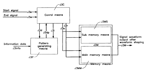
FIG. 15 is a schematic block diagram illustrating basic
configuration of the first, second, third, and fourth
embodiment of the waveform shaping equipment according to
the present invention.
To the input of the pattern generator J3P, information
26
CA 02305706 2000-OS-04
data J3info is successively inputted from outside of the
waveform shaping equipment, and at the pattern generator
J3P, dummy data J3d generated from the control means J3c is
added to the head and the trail of the information data
string J3info to form a packet with dummy data, and part of
the packet with dummy data is extracted to generate the data
pattern J3dp. To the control means J3C, the transmission
status signal which advises the presence of information data
J3info is inputted from outside of the waveform shaping
equipment as start signal J3s and end signal J3e. The start
signal J3s is a signal to input the pulse wave for
triggering as soon as the head of the information data
J3info is inputted and the end signal J3e is a signal to
input the pulse wave for triggering as soon as the trail of
the information data J3info is inputted. The control means
J3C generates dummy data J3d for the pattern generator J3P
for a specified period a specified time after these start
signal J3s/end signal J3e are inputted. The control means
J3C generates input control signal J3i, output control
signal J3o, and readout signal J3r based on the data pattern
J3dp and start signal J3s/end signal J3e. The input control
signal J3i is a control signal for allowing the pattern
generator J3P to select either information data J3info or
dummy data J3d and to constitute a packet with dummy data,
the output control signal J3o is a control signal for
selecting either main memory means J3MM or sub-memory means
J3SM in the memory means J3 to be used for each sequence.
and the readout signal J3r is a signal to serve as an
address for specifying partial waveform to be read out from
27
CA 02305706 2000-OS-04
the main memory J3MM and the sub memory means J3SM,
respectively. The output control signal J3o and readout
signal J3rare inputted to the main memory means J3MM and the
sub memory means J3SM, which read out partial waveform using
part of the output control signal J3o and readout signal
J3r, respectively. The read out partial waveform is
concatenated successively at the output section of each
memory means and the signal waveform J3w which has the
waveform shaped is outputted.
FIG. 16 is a schematic block diagram illustrating
exemplary configuration of the waveform shaping equipment in
which the memory means comprises a semiconductor memory,
data selector, buffer, D/A converter, and filter, the
pattern generator comprises a delay unit, data selector, and
shift register, and the control means comprises a clock
generator, counter, sequencer, comparing unit, and dummy
data generator in FIG. 15.
Description on FIG. 16 is made as follows.
In the pattern generator J4P, the information data
J4info delayed for a certain time (D = KT) from the point
where the start signal J4s is applied is inputted to the
data selector J4PS1 by the dummy data J4d or the delay unit
J4PD. The delay unit J4PD comprises a shift register. The
data selector J4PS1 is selected by the input control signal
J4i, and inputs dummy data J4d when the dummy data J4d is
generated,or otherwise, inputs the delay unit output J4PD to
the shift register J4PSf. The shift register J4PSf shifts
every unit time T in synchronism with the data clock (1/T).
The parallel output of the shift register J4PSf generates
28
CA 02305706 2000-OS-04
the data pattern J4dp with the output having w bits. This
data pattern J4dp is inputted to the control means J4C and
inputted to the main memory table J4MM and sub memory table
J4SM as it is as part of the readout signal J4r.
In the control means J4C, the counter J4CCo operates on
the sampling clock (1/t> generated at the clock generation
circuit J4CCk. The output of this counter J4CCo shows the
sampling point in the present time slot and forms, as it
is,part of the readout signal J4r for instructing the
address of each memory table. The sequences J4CS operates
in synchronism with the data clock which is divided by 2~n
for the sampling clock (1/t) generated by the clock
generation circuit J4CCk, and holds the transition state
every unit time T after the start signal J4s/end signal J4e
are applied for a predetermined period. The comparing unit
J4CCp compares the information in the comparing unit with
the output of the counter J4CCo and that of the sequences
J4CS, generates the input control signal J4i and output
control signal J4o as well as readout signal J4r and
internal control signal j4ci, and times each sequence. The
dummy data generator J4CD generates the acknowledge signal
J4a and the dummy data J4d to be used at intervals of unit
time T based on the internal control signal J4ci from the
comparing unit J4CCp.
In the memory means J4M, the main memory means is
designated as the main memory table J4MM and sub memory
means as the sub memory table J4MS. To the main memory
table J4MM which is accessed in the ordinary sequence,
partial waveforms of baseband signal waveforms after
29
CA 02305706 2000-OS-04
and limitation for all binary patterns are written. To the
sub memory table J4MS accessed in the spare sequence,
partial waveforms of the baseband signal waveforms after
bandlimitation are written with respect to ternary patterns
for every unit time T shift of the dummy data to be used.
The period of this spare sequence is determined by the
pattern length w. To the main memory table J4MM and the sub
memory table J4MS, the readout signal J4r generated at the
control means J4C is inputted, and to the data selector
J4MS, the output control signal J4o generated at the control
means J4C is inputted. respectively. The main memory table
J4MM reads out partial waveform utilizing the output of the
counter J4CCo, which is part of the readout signal J4r, and
the data pattern J4dp. In the similar manner, the sub
memory table J4MS reads out partial waveform utilizing the
output of the counter J4CCo, which is part of the readout
signal J4r, the data pattern J4dp, and sub memory table
control signal. The read out partial waveform is
concatenated successively at the output section of the
buffer J4MB by selecting the data selector J4MS1 with the
output control signal in accordance with each sequence as
well as sampling and holding at the buffer J4MB. The
concatenated signal waveform is smoothed by the filter J4MF
after it passes the D/A converter J4MD and the baseband
signal waveform J4w after bandlimitation is generated. Now,
if the dummy data string to be used is specified, because it
is only required to read out partial waveform of the
baseband signal after bandlimitation with respect to the
constantly fixed pattern for the spare sequence sequentially
CA 02305706 2000-OS-04
from the sub memory table J4MS, the memory capacity of the
sub memory table J4MM to be used for the spare sequence can
be greatly reduced by preparing a decoder J4MDc at the sub
memory table input section and carrying out the readout in
accordance with part of the readout signal J4r.
FIG. I7 illustrates an exemplary configuration of a
control means when the sequences J4CS of the control means
of FIG. 16 is formed with a shift register JSSf, edge
detection circuits JSEgs, JSEge, and a latch JSLt, the
comparing unit J4CCp with a comparator JSCCp, buffer JSCB,
and information table JSCI, and the dummy data generator
J4CD with a decoder JSDD and ROM JSDR.
Now FIG. 17 is described as follows.
The clock generation circuit JSCk generates the
sampling clock (1/t) for realizing the sampling interval t
of 2"n partial waveforms in 1 time slot. This sampling
clock forms the operation clock of the counter JSCo.
The counter JSCo has n-bit output, its MSB is the clock
with the sampling clock (1/t) generated by the clock
generation circuit JSCk divided by 2"n, and serves as the
data clock (1/T> for the entire waveform shaping equipment.
The n-bit output of the counter JSCo indicates the sampling
point in the present time slot and is inputted to the
comparing unit JSCC.
In the sequences JSS, the shift register JSSf operates
in synchronism with the data clock (1/T>. At the input
section of the sequences JSS, there are edge detection
circuit sJSEgs, JSEge which detect the rising edges of the
start signal and end signal, respectively, and generates
31
. CA 02305706 2000-OS-04
specified pulses. The output of the edge detection circuit
JSEgs is inputted to the set side of RS latch 5J5Lt on the
next stage, and the output of the edge detection circuit
JSEge is inputted to the reset side of the RS latch SJSLt,
respectively. The output of the RS latch JSLt is inputted
to the shift register, and when the start signal is
inputted, it inputs the logical value "1" to the shift
register JSSf and when the end signal is inputted, it inputs
the logical value "0". The number of shifts L of the shift
register JSSf requires the number enough to express all the
transition states for each unit time T in the spare
sequence, and the parallel output of the shift register J5Sf
is inputted to the comparing unit JSCC.
In the comparing unit J5CC, the information table JC5
control information which is compared in extracting timing
of the comparator JSCCp. The comparator JSCCp takes out the
positional information of the change-over edge between the
logical values "1" and "0" from the output of the sequencer
J5S and extracts timing by collating the positional
information and the output of the counter J5Co with the
information table JSI. In addition, comparator JSCCp has a
decoder inside and based on the extracted timing, it
generates input control signal JSi, output control signal
JSo, readout signal JSr, and internal control signal JSci.
The readout signal J5i comprises data pattern J5dp and
output of counter JSCo.
In the dummy data generator JSD, the decoder JSDD
outputs address signal JSDa for reading out dummy data J5d
to be used from ROM table JSdr and enable signal JSDe for
32
CA 02305706 2000-OS-04
controlling generation and stopping of dummy data JSd. In
addition, the decoder JSDD returns the acknowledge signal
J5a for informing the receipt of the start signal J5s and
end signal J53. The dummy data J5d read out from ROM table
JSDR is outputted successively to the pattern generation
circuit at every time intervals T.
Referring now the configuration drawings of FIG. 16 and
FIG. 17, the first, second, and third embodiments are
described.
FIG. 18 illustrates a time sequence expressing a data
pattern forming process in the first embodiment according to
the present invention when the hardware is configured based
on the schematic block diagrams shown in FIG. 16 and FIG.
17. In the first embodiment, the pattern length w is 5 and
dummy data string 4 bits, and ~1, -1, 1, -1} is used for the
predummy data and ~-1, 1, -1, 1} for the postdummy data.
Now, the specific description will be made on the
generation timing of the input control signals, output
control signals, and readout signals from the comparing unit
in the case of this first embodiment.
In this first embodiment, D (k> (k = 1, ..., n) denotes
the information data. Each 1T, 2T, ..., (n + 14>T shows the
elapsed time for every unit time T, and A (1), A (2>, ..., A
(5) denote each time slot in the pattern, respectively.
Now, the present time slot is A (3). In this first
embodiment, the number of shifts of the delay unit is
designated asK = 4 and the number of shifts of the shift
register as L =9.
Observation of the time sequence shown in FIG. 18
33
. ~ CA 02305706 2000-OS-04
indicates that time 1T to 5T and time (n + 10)T to (n + 14)T
coincide with the spare sequence containing data value 0 and
time 6T to (n + 9)T with the ordinary sequence comprising
binary values of 1 and -1. In the period from time 2T to
5T, the dummy data corresponding to the predummy data is
generated from the dummy data generator, while in the period
from time (n + 6)T to (n + 9)T, the dummy data corresponding
to the post dummy data string is generated. The input
control signal generated by the comparing unit selects the
data selector in the pattern generator and allows the shift
register in the sequencer to input the dummy data during
this period. Because in this first embodiment, the dummy
data string to be used is specified to one set and no
information data is always included in the pattern during
the spare sequence, the partial waveform is read out by a
constantly fixed pattern. That is, in the time section 1T
of the spare sequence, it is allowed to read out partial
waveforms by the pattern ~0, 0, 0, 0, 0} in the time section
1T of the spare sequence and by the pattern {0, 0, 0, 0, 1}
in the time section 2T of the spare sequence, and this same
principle applies to the time section 3T, 4T, 5T, (n + 10)T,
(n + 11)T, (n + 12)T,(n + 13)T, and (n + 14)T. Therefore,
in the spare sequence, the comparing unit combines the sub
memory table control signals obtained by decoding the
parallel output of the shift register with the counter
output, generates the readout signal for sub memory table
access, and reads out partial waveforms. In the ordinary
sequence, the comparing unit combines the data pattern and
counter output as it is, generates the read out signal for
34
CA 02305706 2000-OS-04
main memory table access, and reads out partial waveforms.
The control signal generated by the comparing unit may
change over the data selector from the sub memory table to
the main memory table at the timing of time 5T to 6T and
from sub memory table to main memory table at the timing of
time (n + 9>T to (n + 10) T. In this first embodiment, the
period of the ordinary sequence from 8T to (n + 7)T has the
information data contained in the present time slot A(3),
which is actually the transmission of information data.
FIG. 19 illustrates a time sequence representing the
forming process of the data pattern in the second embodiment
according to the present invention when the hardware is
configured based on the configuration drawings shown in FIG.
16 and FIG. 17. In the second embodiment, the pattern
length w is 5 and dummy data string 2 bits, and ~1, -1} is
used for the predummy data and {-1, 1} for the postdummy
data.
Now, the specific description will be made on the
generation timing of the input control signals, output
control signals, and readout signals from the comparing unit
in the case of this second embodiment.
In this second embodiment, D (k) (k = 1, ..., n)
denotes the information data. Each 1T, 2T, ..., (n + 10>T
shows the elapsed time for every unit time T, and A (1), A
(2>, ..., A (5) denote each time slot in the pattern,
respectively. Now, the present time slot is A (3). In this
second embodiment, the number of shifts of the delay unit is
designated as K = 2 and the number of shifts of the shift
register as L= 7.
CA 02305706 2000-OS-04
Observation of the time sequence shown in FIG. 19
indicates that time 1T to ST and time (n + 6)T to (n + 10>T
coincide with the spare sequence containing data value 0 and
time 6T to (n + 9>T with the ordinary sequence comprising
binary values of 1 and -1. In the period from time 2T to
3T, the dummy data corresponding to the predummy data is
generated from the dummy data generator, while in the period
from time (n + 4)T to (n + 5)T, the dummy data corresponding
to the post dummy data string is generated. The input
control signal generated by the comparing unit selects the
data selector in the pattern generator and allows the shift
register in the sequences to input the dummy data during
this period. Because in this second embodiment, the dummy
data string to be used is specified to one set and no
information data is included in the pattern in the time
section 2T, 3T and time section (n + 8)T, (n + 9>T in the
spare sequence, the comparing unit combines the sub memory
table control signals obtained by decoding the parallel
output of the shift register with the counter output,
generates the readout signal for sub memory table access,
and reads out partial waveforms. In the time sections 4T,
5T and time sections (n + 6)T, (n + 7)T, because the
information data is included in the pattern, the read out
signal waveforms depend on the information data included in
it. Therefore, in this period, the comparing unit combines
the sub memory table control signals obtained by decoding
the parallel output of the shift register and part of data
pattern and counter output to generate the readout signal,
and reads out partial waveforms from the sub memory table
36
CA 02305706 2000-OS-04
using it as an address. In the ordinary sequence, the
comparing unit combines the data pattern and counter output
as it is, generates the readout signal for main memory table
access, and reads out partial waveforms. The output control
signal is only required to change over the data selector
from the sub memory table to the main memory table at the
timing of time 5T to 6T and from sub memory table to main
memory table at the timing of time (n + 5>T to (n + 6) T.
In this second embodiment, the information data is
transmitted during the period from time 6T to time (n+5)T.
In this second embodiment, the hardware of the control means
becomes complicated as compared to the first embodiment, but
the time required from the start to the end of transmission
of information data can be shortened by 2 time slots.
In these first and second embodiments, discussion was
made on the case when the pattern length (w=5) is an odd
number, but the same principle can be applied to the case
when the pattern length w is an even number.
FIG. 20 illustrates a time sequence expressing a data
pattern forming process in the third embodiment according to
the present invention when the hardware is configured based
on the schematic block diagrams shown in FIG. 16 and FIG.
17. In the third embodiment, the pattern length w is 4 and
dummy data string 3 bits, and {1, -1, 1} is used for the
predummy data and {-1, 1, -1} for the postdummy data.
Now, the specific description will be made on the
generation timing of the input control signals, output
control signals, and readout signals from the comparing unit
in the case of this third embodiment.
37
CA 02305706 2000-OS-04
In this third embodiment, D (k) (k = 1, ..., n) denotes
the information data. Each 1T, 2T, ..., (n + 11)T shows the
elapsed time for every unit time T, and A (1), A (2>, A (3),
A (4) denote each time slot in the pattern, respectively.
Now, the present time slot is located between A (2) and A
(3> so that the effects of each data in the pattern before
and after the present time slot on the present time slot
becomes uniform. In this third embodiment, the number of
shifts of the delay unit is designated as K = 3 and the
number of shifts of the shift register as L = 7.
Observation of the time sequence shown in FIG. 20
indicates that time 1T to 4T and time (n + 8>T to (n + 11)T
coincide with the spare sequence containing data value 0 and
time 5T to (n + 7)T with the ordinary sequence comprising
binary values of 1 and -1. In the period from time 2T to
4T, the dummy data corresponding to the predummy data is
generated from the dummy data generator, while in the period
from time (n + 5)T to (n + 7)T, the dummy data corresponding
to the post dummy data string is generated. The input
control signal generated by the comparing unit selects the
data selector in the pattern generator and allows the shift
register in the sequencer to input the dummy data during
this period. Because in this third embodiment as well, the
dummy data string to be used is specified to one set and no
information data is always included in the pattern during
the spare sequence, the partial waveform is read out by a
constantly fixed pattern, which is the same as in the case
of the first embodiment. The output control signal
generated by the comparing unit may change over the data
38
CA 02305706 2000-OS-04
selector from the sub memory table to the main memory table
at the timing of time 4T to 5T and from sub memory table to
main memory table at the timing of time (n + 7)T to (n + 8)
T. In this embodiment, the information data is transmitted
in the period from time 6T to (n+ 6)T.
As described above, in these first, second, and third
embodiments, the sequences is formed by the use of a shift
register, but the same effects can be obtained even when the
sequences is formed by the use of a counter.
FIG. 21 is a schematic block diagram illustrating the
exemplary waveform shaping equipment when as compared with
FIG. 15, the memory means is formed with a semiconductor
memory, buffer, D/A converter, and filter, the pattern
generator is formed with a shift register only, and the
control means is formed with a clock generation circuit,
counter, shift register, address decoder, comparator,
information table, and buffer.
Referring now FIG. 21, preferred embodiments will be
described.
In the control means J9C, the clock generation circuit
J9CCk generates sampling clock (1/t) for realizing sampling
intervals t of 2~n pieces of partial waveforms during one
time slot. This sampling clock (1/t) becomes the operation
clock for the counter J9CCo. The counter J9CCo has n-bit
outputs and MSB of the output becomes the data clock (1/T).
Then-bit output of the counter J9CCo indicates the sampling
point in the present time slot and constitutes part of read
out signal J9r for indicating the address of the memory
table.
39
CA 02305706 2000-OS-04
The output of the counter J9CCo is inputted also to the
comparator J9CCp. To the buffer J9CB, the start/end signal
J9se is inputted. In this start/end signal J9se, the change
from logic value "0" to logic value "1" indicates the input
of the start signal, while the change from logic value "1"
to logic value "0" indicates the input of the end signal.
This output of the buffer J9CB is inputted to the pattern
generator Jo as the input control signal J9i. The ternary
data pattern J9dp generated at the pattern generator J9P is
inputted to the address decoder J9CA and the address decoder
J9CA generates part of the readout signal J9r for access to
the memory table in the memory means based on this ternary
data pattern. The comparator J9CCp generates the acknowl-
edge signal J9a to outside the waveform shaping equipment by
collating the output of the counter J9CCo and part of the
data pattern J9dp from the pattern generator J9P with the
information table J9CI.
In the pattern generator J9P, two shift registers shift
in synchronism with the data clock (1/T). To the shift
register J9PS1, the information data J9info is inputted. To
the shift register J9PS2, the input control signal J9i is
inputted through the buffer J9Pb in the control means, and
the transition state every unit time T after application of
the start/end signal J9se is maintained. The parallel
outputs of the shift register J9PS1 and shift register J9PS2
have the number of outputs equivalent to the pattern length
w. The parallel outputs of these two shift registers are
combined in two pairs, respectively, in order of time ser-
ies, forming the ternary data pattern J9dp which is ex-
CA 02305706 2000-OS-04
pressed with 2 bits. Each 2 bits of this ternary data pat-
tern J9dp are designed to take the data value 0 irrespective
of the logic value of the shift register J9PS21 when the
logic value of the shift register J9PS2 is "0," and when the
logic value of the shift register J9PS2 is "1" and that of
the shift register J9SP1 "1," they take the data value 1,
and when the logic value of the shift register J9PS2 is "1"
and that of the shift register J9SP1 "0," they take the data
value -1.
In the memory means J9M, the common memory table J9MC
is formed by integrating the main memory table with the sub
memory table. To the common memory table J9MC, all partial
waveforms of baseband signals after bandlimitation are
stored. The readout signal J9r generated from the control
means J9C is formed by combining the signal generated from
the address decoder J9CA with the output of the counter
J9CCo. The common memory table J9MC reads out partial
waveforms of baseband signals after bandlimitation using
this readout signal J9r as an address, and the read out
partial waveform is sampled and held at the buffer J9MB to
be concatenated successively at the output section of the
buffer J9MB. The concatenated signal waveform is smoothed
by the filter J9MF after it passes the D/A converter J9MD
and the baseband signal waveform after bandlimitation is
formed.
Referring now to the schematic block diagram of FIG.
21, the fourth embodiment will be explained.
FIG. 22 illustrates a time sequence expressing a data
pattern forming process in the fourth embodiment according
41
~
. CA 02305706 2000-OS-04
to the present invention when the hardware is configured
based on the schematic block diagrams shown rn FIG. 21. In
the fourth embodiment, the pattern length w is 5 and no
dummy data string is used.
Now, the specific description will be made on the
fourth embodiment.
D (k) (k = 1, ..., n) denotes the information data.
Each 1T, 2T, ..., (n + 6)T denotes elapsed time for every
unit time T, and A (1), A (2), A (3), A (4), A (5) denote
each time slot in each pattern. Now, the present time slot
is A (3). Observation of the time sequence shown in FIG. 22
indicates that time 1T to 5T and time (n + 2>T to (n + 6)T
coincide with the spare sequence containing data value 0 and
time 6T to (n + 1)T with the ordinary sequence comprising
binary values of 1 and -1. In the common memory table,
partial waveforms of all baseband signals before and after
bandlimitation for ternary patterns are retained. It is,
therefore,only required to read out partial waveforms of
baseband signal of ter bandlimitation with the readout signal
generated from the control means used for the address. In
this fourth embodiment, from time 4T to (n + 3)T period, the
present time slot contains the information data, which means
that the information data is being transmitted. In this
fourth embodiment, the hardware scale with respect to the
shift register, address decoder, memory, etc. increases but
no complicated control means is required to change over the
memory table and the dummy data string is not necessary to
generate. In the fourth embodiment, it is possible to input
the information data into the shift register in the pattern
42
CA 02305706 2000-OS-04
generator from the first time without using dummy data, and
the time equivalent to several time slots required for
transmitting dummy data strings can be shortened. In the
case of this fourth embodiment, the ternary patterns were
described but the same principle will be applied to
multilevel patterns exceeding ternary patterns, if an
address decoder for converting multilevel patterns to binary
address signals is provided, partial waveforms of baseband
signals after bandlimitation are found by calculation for
the number of all combinations, and the results are written
in the common memory table.
In these embodiments, the profile of the baseband
signal waveform before bandlimitation for expressing each
transmission data is not limited only to rectangular wave-
form but may be optional. In addition, the present inven-
tion is not limited only to baseband signal waveform shaping
but may be applied to modulated waveform shaping.
43
. ~ CA 02305706 2000-OS-04
FIG. 23 is a schematic block diagram illustrating a
waveform shaping equipment in the fifth embodiment of the
present invention. In FIG. 23, J111 denotes a pulse
waveform generating means, which comprises an address
generating means J117 and memory tables J115 and J116. The
address generating means J117 comprises a shift register
J118 and counter J119. J112 denotes a waveform processing
means, which comprises a waveform adding means J113, wave-
form selecting means J114, and selecting signal generating
means J1111. J1110 is a D/A converter. Jlld denotes data
strings, Jlldl and Jlld2 are the first-stage output and the
second-stage output of the shift register J118, respective-
ly, Jllc is a counter output, J11w0 is a zero-level wave-
form, Jllwl is the first waveform, Jllw2 is the second
waveform, Jllw3 is the third waveform, Jllw4 is a shaped
waveform, Jllb is a burst control signal, Jlls is a
selecting signal, and Jllw5 is an analog signal. Now, each
symbol of data string Jlld is a binary symbol of either 0 or
1 and is transmitted bit by bit per one symbol time. The
burst control signal Jllb controls the start and the end of
the data string to be transmitted of the data string Jlld.
FIG. 24 illustrates the waveform data which is stored
in advance in the memory tables J115 and J116. In the
memory table J115, the first waveform data shown in FIG. 24-
a and FIG. 24-b and the second waveform data shown in FIG.
24-c and FIG. 24-d are stored. However, the first and the
second waveforms are waveforms for the first half and the
second half of the pulses for 1 symbol data, respectively.
In this event, a positive polarity pulse is used for the
44
CA 02305706 2000-OS-04
data "0" and a negative polarity pulse is used for the data
"1." For the pulse for one symbol data, the waveform which
converges within two symbol times in all is assumed. Each
waveform data comprises 8 sample data per 1 symbol time.
Consequently, memory tables J115 and J116 store a total of
16 samples each of data, 8 samples for 1 symbol time for
data "0" and 8 samples for 1 symbol time for data "1,"
respectively.
In FIG. 23, the data string Jlld is first inputted to
the shift register J118. The shift register J118 shifts the
data every 1 symbol time and outputs in parallel the first-
stage output Jlldl and the second-stage output Jlld2. In
the following description, one symbol time from the point in
]which the shift register J118 shifts the data to the point
in which it shifts the data next is called the symbol
interval. The counter J119 is a 3-bit counter which counts
up every one-eighth symbol time and repeats counting at the
intervals of 1 symbol time. The counter output Jllc is a 3-
bit binary symbol which counts up successively from "000" to
"111"in each symbol interval. The addressing signal gener-
ating means J117 comprises a shift register J118 and a
counter J119, and feeds 4-bit address with the most signifi-
cant bit as Jlldl and Jlld2 and three low-order bits as Jllc
to memory tables J115 and J116, respectively.
With the address generated as above, the memory tables
J115 and J116 output the first waveform Jllwl and the second
waveform Jllw2. The first waveform Jllwl takes the waveform
data of FIG. 24-a and FIG. 24-b successively from the left
when Jlldl is "0" and "1," respectively, in each symbol
CA 02305706 2000-OS-04
interval. The second waveform Jllw2 takes the waveform data
of FIG. 24-c and FIG. 24-d successively from the left when
Jlld2 is "0" and "1, "respectively, in each symbol interval.
The wav.eform adding means J113 adds the first waveform
Jllwl and the second waveform Jllw2 and outputs the third
waveform Jllw3. The waveform selecting means J114 inputs
the first waveform Jllwl, the second waveform Jllw2, the
third waveform Jllw3 and the zero-level waveform J11w0,
selects either one in accordance with the selecting signal
Jlls, and outputs it as shaped waveform Jllw4. In this
event, the zero-level waveform J11w0 is a waveform whose
value is constantly zero; for example, when two's-complement
representation is used, this can be achieved by constantly
bringing all bits to zero.
FIG. 25 illustrates waveforms of each section of the
waveform shaping equipment of FIG. 23. In FIG. 25. signals
taking digital values are expressed by converting them into
analog values.
In FIG. 25, of the data strings Jlld, the portion of
information data info is the data to be transmitted, which
occurs in the burst form. The burst control signal Jllb is
a signal for indicating the start and the end of data to be
transmitted and becomes a high level during the period from
the start to the end of information data info and in the
period other than the above. it becomes low level. The
contents of the data string before and after the information
data info may be optional, but in this embodiment, operation
will be described with the contents all designated to zero
for convenience.
46
~
~ CA 02305706 2000-OS-04
The data string Jlld is inputted into the shift
register J118 and the data for the latest 2 bits is
retained. From the memory table JliS, the first half of
either positive polarity or negative polarity pulses are
outputted in accordance with the first-stage output Jlldl of
the shift register J118. Because in this event Jlld2 varies
1 symbol time delayed from Jlldl~ the polarity change of the
second waveform occurs 1 symbol time delayed with respect to
the polarity change of the first waveform jllwl as shown in FIG.
25. That is, in each symbol interval, the second waveform jiiw2
represents the latter half of the pulse corresponding to the
preceding data and the first waveformjllwl the first half of the
pulse corresponding to the succeeding data.
The third waveform Jllw3 which is the sum of the first
waveform Jllwl and the second waveform Jllw2 represents the
waveform generated by interference between the preceding and
succeeding data in each symbol interval, and covers the area
from the center of the pulse corresponding to the preceding
data and the center of the pulse corresponding to the
succeeding data. Consequently, the waveform successively
arranging the third waveforms generated in each symbol
interval is the waveform superimposing pulses corresponding
to each symbol of the data string Jlld, and is a waveform
shaped output for the continuous data.
Next description will be made on the operation.at the
start and the end of the information data info. The
selecting signal generating means J1111 generates the
selecting signal Jlls and controls operation of the waveform
selecting means J114. The selecting signal-Jlls is, in
47
~
~ CA 02305706 2000-OS-04
general, a 2-bit signal and the four kinds of values which
the signal can take are now expressed as 0, 1, 2, 3. The
waveform selecting means J114 selects the zero level signal
J11w0 when the selecting signal Jlls is 0, the first wave-
form Jllwl when it is 1, the second waveform jllw2 when it
is 2, and the third waveform Jllw3 when it is 3, respective-
ly, and outputs them as Jllw4. The selecting signal Jlls
takes 1 in the symbol interval just after the start of the
information data info, 3 from the next symbol interval to
the end of information data info, and 2 from the end of
information data info to the next symbol interval as shown
in FIG. 25. And in the area other than the above, it takes
0: Therefore, the shaped waveform Jllw4, which is the
selector output, is a zero-level waveform J11w0 up to the
start of the information data info, and the waveform smooth-
ly rises from the zero level because from the start of the
information data info to 1 symbol time the waveform becomes
the first waveform which is the first half of the pulse for
the first bit. Thereafter to the end of the information
data info, the third waveform occurs and from the end of the
information data info to one symbol time, the second wave-
form which is the latter half of the pulse for the last
pulse is generated. This causes the waveform to converge to
the zero level with a smooth trailing. Thereafter the
waveform becomes the zero-level signal J11w0 again.
With the above operation, the shaped waveform Jllw4
becomes smoothly shaped waveform throughout the whole period
including the start and the end of the data to be
transmitted in transmission of burst-like information data.
48
CA 02305706 2000-OS-04
Lastly, the D/A converter J1110 converts the shaped waveform
Jllw4, which is a digital signal waveform, to an analog
waveform and obtains a smoothly shaped burst-like analog
output JllwS.
In the above fifth embodiment, the first and the second
waveforms are designated to be simple positive-polarity or
negative-polarity pulses as shown in FIG. 24, but they are
not limited to these but may be more complicated pulse
waveforms or modulated waveforms. The data string Jlld is
designated to be the binary string of either "0" or "1," but
it is not limited to these, but may be multilevel symbols.
For example, if the data string Jlld is a string of 2"M
level symbol, the shift register J118 is configured in M bit
x 2 stages and Jlldl and Jlld2 become M-bit signals, respec-
tively. The first and the second waveform are designated to
have8 samples per 1 symbol time but they are not limited to
these but may have optional number of samples. In order to
express the start and the end of the data string to be
transmitted, the burst-like control signal Jllb is designed
to be used but other methods may be used; for example, a
method to feed data start signals and data end signals
separately or a method to multiplex information of the
starting time and ending time in the data string itself may
be used.
In the above fifth embodiment, if the present invention
is applied to continuous data transmission, not to burst
transmission, it can be designed to eliminate the waveform
selecting means J114 and the selecting signal generating
means J1111 and to constantly D/A convert the third waveform
49
~
~ CA 02305706 2000-OS-04
Jllw3.
Next, the sixth embodiment will be described. FIG. 26
is a schematic block diagram illustrating a waveform shaping
equipment in the sixth embodiment of the present invention.
In FIG. 26, J141 denotes a waveform adding means which
comprises an adder J1430 and latches J1412, J1413. J1414
denotes a cut-off signal generating means. The waveform
processing means J142 comprises with these components.
Because other portions are the same as those of the fifth
embodiment in FIG. 23, the description on which will be
omitted.
FIG. 27 illustrates the signal waveform of each portion
of the waveform shaping equipment of FIG. 26. In FIG. 27,
signals taking digital values are converted to analog values
for indication.
In FIG. 26, latches J1412 and J1413 uses the first
waveform Jllwl and the second waveform Jllw2 as input sig-
nals, respectively, and outputs signals same as those of
input signals or zero-level signals in accordance with the
reset signals J14r1 and J14r2. That is, they assume respon-
sibility for cutting off the inputs to the waveform adding
means J143, respectively. In this case, J14r1 and J14r2 are
assumed to be positive logic reset signals. That is, the
output J14w10 of latch J1412 becomes Jllwl when J14r1 enters
low level, and enters zero level when it enters high level,
and similarly, the output J14w20 of latch J1413 becomes
Jllw2 when J14r2 enters low level, and zero level when it
enters high level.
The cut-off signal generating means J1414 generates
CA 02305706 2000-OS-04
reset signals J14r1 and J14r2 as shown in FIG. 27 from
timing of the change of burst control signal Jllb. This
brings the input of the waveform adding means J143 partially
to the zero level and controls the output waveform of the
adder. First of all, up to the start of information data
info, both J14r1 and J14r2 are at the high level. At the
start of information data info, J14r1 changes to low level
but J14r2 is held to high level and after the next symbol
interval, both J14r1 and J14r2 change to high level.
Consequently, as shown FIG. F15, J14w10 becomes the first
waveform in the interval from the start to the end of the
information data info, and in other intervals, changes to
zero level. J14w20 becomes the second waveform in the
interval from the next symbol interval of the start of the
information data info to the next symbol interval of the end
of the information data info, and in other intervals,
changes to zero level.
The adder J1430 adds J14w10 and J14w20 and obtains
shaped waveform J14w4 as an output. As clear from FIG. 25
and FIG. 27, this is identical to that of shaped waveform
llw4 in the fifth embodiment. That is, it becomes the first
waveform during 1 symbol time from the start of information
data info and smoothly rises, and thereafter to the end of
information data info, it becomes the third waveform which
is the sum of the first and the second waveforms, and then,
smoothly falls as the second waveform for 1 symbol time from
the end of information data info. Finally, D/A converter
J1110 converts the shaped waveform Jl4wk, which is a digital
signal waveform, to analog waveform and obtains the analog
51
~
CA 02305706 2000-OS-04
output same as that of the fifth embodiment.
By the way, in the sixth embodiment described above,
latches J1412 and J1413 are used to bring J14w10 and J14w20
to zero level, but any circuits other than latches can be
used if they can control passing and cut-off of input of the
waveform adding means J143; for example, a circuit which
fixes either one of the two input selectors to zero level
may be used.
Next discussion will be made on the seventh embodiment.
FIG. 28 illustrates a block diagram of the waveform shaping
equipment of the seventh embodiment according to the present
invention. The waveform shaping equipment of this
embodiment is designed to generate band-limited two baseband
signals to be applied for quadrature modulation such as
quadrature phase shift keying. In FIG. 28, J1615 is a
serial-parallel converter, J168I and J168Q are shift regis-
ters, J165I,J166I, J165Q and J166Q are memory tables,
J1612I, J1613I, J1612Q and J1613Q are latches, J1614 is a
cutoff signal generating means, J1630I and J1630Q are ad-
ders, J1610I and J1610Q are D/A converters. In FIG. 28,
data string Jlld is converted to 2-bit serial data strings
by the serial-parallel converter J1615 and one data string
is fed to the shift register J168I and the other to the
shift register J168Q. After two shift registers J168I and
J168Q, two systems of the circuit basically similar to the
wave shaping equipment of FIG. 26 in the sixth embodiment
and generate waveforms of baseband signals for in-phase axis
(I axis) and those for quadrature axis (Q axis), re-
spectively.
52
~
CA 02305706 2000-OS-04
What differs from the equipment of FIG. 26 is that both
outputs of two systems of shift register J168I and J168Q are
fed as address of the memory table. In this embodiment,
because one symbol data comprises 2 bits, the relevant
waveform generating means have four types of waveform data
for one symbol time comprising 8 samples, respectively, and
selects either one type by combining 2-bit data for output.
The counter J169 and cutoff signal generating means J1614
are same as those shown in FIG. 26 in the sixth embodiment,
and these outputs can be shared in the circuits for I axis
and Q axis, thereby allowing only one 5'ystem to be provided.
As described above, the present invention is also
suited for application where waveform shaping is carried out
for baseband signals for quadrature modulation or multi-
level modulation in carrier transmission.
Now, the eighth embodiment is described. FIG. 29 is a
block diagram illustrating the pulse waveform generating
means in the waveform shaping equipment in the eighth embod-
invent according to the present invention. Portions other
than the pulse waveform generating means are same as those
of the fifth embodiment. In FIG. 29, J1716 is a memory
table, J1717, J1718 are shift registers for waveform data,
J1719 is a timing generator, and J1720 is a multiplexer.
The shift register J178 is the same as that shown in FIG. 23
in the fifth embodiment. The pulse waveform generating
means J171 comprises the above components. FIG. 30 illus-
trates the timing of signals of each section of FIG. 29.
The memory table J1716 stores only the data equivalent
to FIG. 24-a and FIG. 24-b. What is characteristic in the
53
CA 02305706 2000-OS-04
present embodiment is that as waveform data, the first
waveform and the second waveform are designed to be
symmetrical with regard to time. With this configuration,
even if waveforms equivalent to FIG. 24-a and FIG. 24-b only
are stored, using these inverted with regard to time can
produce waveforms equivalent to FIG. 24-c and FIG. 24-d.
The memory table J1716 has 1-bit address inputs,
according to which 8-sample data of FIG. 24-a and FIG. 24-b
can be outputted in parallel. Shift registers J1717 and
J1718 take in 8-sample waveform data outputted by the memory
table J1716 and output 1 sample at a time while shifting.
Howeve r, these two shift registers shift in the opposite
directions.
The timing generator J1719 generates load signals
J171d1, J171d2 and clock Jl7ck of the timing shown in FIG.
30 and feeds them to shift registers J1717 and J1718.
However,J171d1 and J171d2 are negative logic load signals
and shift registers J1717, J1718 load data in series when
they are at low level. When J171d1 or J171d2 are at high
level, the shift register J1717 or J1718 shifts data at the
rising edge of clock Jl7ck for output. In addition, the
timing generator generates multiplexes control signal Jl7m
and feeds to the multiplexes J1720. The multiplexes J1720
selects either of the first-stage output J17d1 or the sec-
ond-stage output J17d2 of the shift register J178 and out-
puts as J17d3. J17d3 serves as an address of the memory
table J1716. Timing of J17d3 shall conform to that shown in
FIG. 30. However, in the periods other than those stated
J17d1 and J17d2, the value of J17d3 may be indefinite. The
54
- ~ CA 02305706 2000-OS-04
shift registers J1717 and J1718 load waveforms to the rising
edge of each symbol interval in accordance with Jl7dl and
J17d2, and while shifting in the direction opposite to each
other, the waveform data is outputted successively.
With the above mentioned action, the shift register
J1717 outputs waveform of FIG. 24-a or FIG. 24-b as first
waveform J17w1 in accordance with J17d1. The shift register
J1718 outputs waveform obtained by time-inverting FIG. 24-a
or waveform obtained by time-inverting FIG. 24-b as second
waveform J17w2 in accordance with J17d2. In addition, the
memory table J1716 requires only to possess data equivalent
to FIG. 24-a and FIG. 24-b, enabling this embodiment to
reduce the memory table capacity to one half that of the
fifth embodiment.
Now, the ninth embodiment is described. FIG. 31
illustrates the pulse waveform generating means in the
waveform shaping equipment in the ninth embodiment according
to the present invention. Portions other than the pulse
waveform generating means are same as those of the fifth
embodiment. In FIG. 31, J1916 is a memory table, J1921 and
J1922 are multiplexers, J1923 is a timing generator, J1924
and J1925 are counter, and J1926 to J1929 are latches. The
shift register J198 is the same as that shown in FIG. 23 in
the fifth embodiment. The pulse waveform generating means
J191 comprises the above components. FIG. 32 illustrates
the timing of signals of each section of FIG. 31.
In this embodiment as well, the first waveform and the
second waveform are designed to achieve symmetrical
relationship with regard to time same as in the eighth
CA 02305706 2000-OS-04
embodiment, and the memory table J1916 stores only the data
corresponding to FIG. 24-a and FIG. 24-b in the same manner
as in the eighth embodiment. What differs from the eighth
embodiment is that the memory table J1916 has 4-bit address
inputs in the same manner as in the case of fifth to seventh
embodiments and outputs data one sample at a time.
First of all, counters J1924 and J1925 are 3-bit
counters and count up and count down in each symbol
interval, respectively, and generate counter outputs 19c1
and J19c2 as shown in FIG. 32.
Next, the timing generator J1926 generates multiplexes
control signals Jl9m as shown in FIG. 32 and controls
multiplexers J1921 and J1922. With these signals, the
multiplexes J1921 selects J19d1 and J19d2 alternately and
outputs J19d3 shown in FIG. 32. The multiplexes J1922
selects counter outputs Jl9cl and J19c2 alternately and
outputs J19d1 shown in FIG. 32. Using these as addresses,
the memory table J1916 outputs alternately the data of se-
lecting each sample of waveform of FIG. 24-a or FIG. 24-b
corresponding to J19d1 successively from the left and the
data of selecting each sample of waveform of FIG. 24-a or
FIG. 24-b corresponding to J19d2 successively from the
right. That is, it outputs the data corresponding to the
first waveform J19w1 and the data corresponding to the
second waveform J19w2 alternately by time-sharing sample by
sample.
The timing generator J1923 further generates clock
signals J19ck1, J19ck2, and J19ck3 shown in FIG. 32 and
feeds J19ck1 to latch J1926, J19ck2 to latch J1927, J19ck3
56
CA 02305706 2000-OS-04
to latches J1928 and J1929, respectively. The latch 1926
takes in and holds the data corresponding to the first wave-
form at the rising edge of J19ck1 and the latch 1927 takes
in and holds the data corresponding to the second waveform
at the rising edge of J19ck2. Finally, because outputs of
latches J1926 and 1927 have their change timing not synchro-
nized each other, latches J1928 and J1929 align timing of
signals of these two systems at the rising edge of J19ck3
and output the first waveform J19w1 and the second waveform
J19w2, respectively.
As described above, in this embodiment as well, in the
same manner in the eighth embodiment, the memory table
capacity can be reduced to one half from that of the fifth
embodiment. In addition to this, because the first waveform
data and the second waveform data are read alternately from
the memory table sample by sample by time sharing, shift
registers J1717, J1718 of the eighth embodiment can be
eliminated and the circuit can be simplified.
FIG. 33 is a block diagram illustrating a waveform
shaping equipment in the 10th embodiment according to the
present invention. In FIG. 33,J211 denotes a slot
generating means, J212 a sample generating means, J213
selecting signal generating means, J214 an addressing signal
generating means, J215 a first waveform generating means,
J216 a second waveform generating means, J217 a waveform
selecting means, J218 a D/A converter, and J219 a D/A
converter, while J2ldt denotes a data string, J2lc a clock
signal, J2lsp a main slot, J2lnp a sub slot, J2lsa a sample
57
CA 02305706 2000-OS-04
signal, J21a1 the first addressing signal, J21a2 the second
addressing signal, J2lss a selecting signal, J21v1 the first
waveform data, J21v2 the second waveform data, J2lvI an in-
phase waveform data, J2lvQ a quadrature waveform data, J2lwI
an in-phase signal waveform, and J2lwQ a quadrature signal
waveform.
In FIG. 33, at the slot generating means J211, data
string J2ldt and clock signal J2lc are inputted and one
piece of main slot J2lsp and d-1 pieces of sub slot J2lnp
are formed and outputted.
At the sample signal generating means J212, clock
signal J2lc is inputted and n-bit sample signal J2lsa is
generated.
At the addressing signal generating means J214, main
slot J2lsp, sub slot J2lnp, and sample signal J2lsa are
inputted, and (m x d - 1 + n)-bit first addressing signal
J21a1 and the second addressing signal J21a2 are formed and
outputted. At the selecting signal generating means J213,
main slot J2lsp is inputted and 1-bit selecting signal J2lss
is formed and outputted.
At the first waveform generating means J215 and the
second waveform generating means J216, the first addressing
signal J21a1 and the second addressing signal J21a2 are
inputted, respectively. At the first waveform generating
means J215, based on (m x d - 1 + n)-bit first addressing
signal J21a1, L-bit first waveform data J2lvl is read out
from the first waveform memory which stores 2"(m x d - 1)
types of waveform data. At the second waveform generating
means J216, based on (m x d - 1 + n)-bit second addressing
58
CA 02305706 2000-OS-04
signal J21a2, L-bit second waveform data J21v2 is read out
from the second waveform memory which stores 2'(m x d - 1)
types of waveform data.
At the waveform selecting means, first waveform data
J21v1, second waveform data J21v2, and selecting signal
J2lss are inputted. The waveform selecting means comprises
the data selector with functions as shown in FIG. 35, and
allotting the first waveform data J21v1 and the second
waveform data J21v2 by the selecting signal J2lss, it out-
puts the in-phase waveform data J2lvI and the quadrature
waveform data J2lvQ.
The in-phase waveform data J2lvI and quadrature
waveform data J2lvQ are inputted to the D/A converter J218
and D/A converter J219 to form continuous signal waveforms
and are outputted as in-phase waveform J2lwI and quadrature
waveform J2lwQ.
FIG. 34 illustrates a block diagram of the waveform
shaping equipment in the 11th embodiment according to the
present invention. In FIG. 34, J221 denotes a slot gener-
ating means, J222 a sampling signal generating means, J223 a
selecting signal generating means, J224 an addressing signal
generating means, J225 the first domain, J226 the second
domain, J227 a waveform selecting means, J228 the first
waveform synthesis means, J229 the second waveform synthesis
means, J22A a D/A converter, and J22B a D/A converter, while
J22dt denotes a data string, J22c a clock signal, J22sp a
main slot, J22np a sub slot, J22sa a sample signal, J22a1
the first addressing signal series, J22a2 the second
addressing signal series, J22ss the selecting signal series,
59
CA 02305706 2000-OS-04
J22v1 the first waveform data series, J22v2 the second
waveform data series, J22vI an in-phase waveform data
series, J2vQ a quadrature waveform data series, J22sI an in-
phase synthesis waveform data, J22sQ a quadrature synthesis
waveform data, J22wI an in-phase signal waveform, and J22wQ
a quadrature signal waveform.
In FIG. 34, at the slot generating means J221, the data
string J22dt and clock signal J22c are inputted, and s
pieces of main slot J22sp and d-s pieces of sub slot J22snp
are formed and outputted.
At the sample signal generating means J222, clock
signal J22c is inputted and n-bit sample signal J22sa is
generated.
At the addressing signal generating means J224, s
pieces of main slot J22sp, d-s pieces of sub slot J22np, and
sample signal J22sa are inputted, and the first addressing
signal series J22a1 comprising s pieces of first addressing
signals and the second addressing signal series J22a2
comprising s pieces of the second addressing signals are
formed and outputted.
At the selecting signal generating means J223, s pieces
of main slot J22sp are inputted and s-bit selecting signal
J22ss is formed and outputted.
The first domain J225 comprising s pieces of first
waveform generating means has the first addressing signal
series J22a1 inputted and from the first domain J225, the
first waveform data series J22v1 comprising s pieces of
first waveform data is read out and outputted.
The second domain J226 comprising s pieces of second
CA 02305706 2000-OS-04
waveform generating means has the second addressing signal
series J22a2 inputted and from the second domain J226, the
second waveform data series J22v2 comprising s pieces of
second waveform data is read out and outputted.
The waveform selecting means comprises s pieces of data
selector with functions of FIG. 35 with respect to relevant
waveform data and has the first waveform data series J22v1,
second waveform data series J22v2, and selecting signal
series J22ss inputted, and outputs the in-phase waveform
data series J22vI comprising s pieces of in-phase waveform
data and the quadrature waveform data series J22vQ
comprising s pieces of quadrature waveform data based on the
selecting signal series J22ss.
The in-phase waveform data series J22vI and quadrature
waveform data series J22vQ are synthesized by the first
waveform synthesis means J228 and the second waveform
synthesis means J229, respectively, to form the in-phase
synthesis waveform data J22sI and quadrature synthesis
waveform data J22sQ, and are inputted to the D/A converter
J22A and D/A converter J22B and are outputted as in-phase
waveform J22wI and quadrature waveform J22wQ, which are
continuous signal waveforms.
FIG. 36 is a diagram illustrating circuit configuration
of the slot generating means in the 10th and 11th
embodiments. In FIG. 36, J241 denotes an m-bit shift
register, J242 a d-bit shift register with m stages, J24dt
data, J24s a slot, J24sp a main slot, J24np a sub slot,
J24cs a symbol clock, and J24cb a bit clock, while the bit
clock J24cb is a sampling clock signal divided by n and the
61
~
~ CA 02305706 2000-OS-04
symbol clock j24cs is a bit clock J24cb divided by m. The
shift register J241 takes data J24dt every bit clock J24cb
by shifting and holds m-bit data for one symbol. The m-
stage shift register J242 takes in the output of the shift
register J241 every symbol clock J24cs by shifting, and (al,
b2, ..., ml), ..., (ad, bd, ..., md) are outputted in paral-
lel by m x d bits of the data pattern length as each slot
J24s. In this event, s pieces out of d pieces of slot J24s
are formed as the main slot J24sp and the remaining d-s
pieces as sub slot J24nnp and are outputted. In the case of
the 10th embodiment, s = 1.
FIG. 37 is a diagram illustrating circuit configuration
of the selecting signal generating means in the 10th and
11th embodiments. In FIG. 37, J25sp denotes a main
slot,J25ex an EXOR (exclusive OR> circuit and J25ss an s-bit
selecting signal series. The exclusive OR is executed to
the first and second bits from the head of S pieces of main
slot J25sp and the results become 1-bit selecting signals,
and after arranged in the sequence of No. i of the main
slot, they are outputted as s-bit selecting signal series
J25ss. Because in the case of the 10th embodiment, s = 1,
they are outputted as 1-bit selecting signals J25ss.
FIG. 38 illustrates an entire block diagram of the
addressing signal generating means in the 10th and 11th
embodiments. In FIG. 38, J261 denotes the first bit
operation circuit, J262 the second bit operation circuit,
and J263 a decoding pattern generating circuit, while J26sp
denotes s pieces of main slot, J26np d-s pieces of sub slot,
J26npg a sub slot group, J26df a decoding pattern, J26p1 the
62
~
CA 02305706 2000-OS-04
first address pattern, J26pn the second address pattern,
J26sa a sample signal, J26a1 the first addressing signal,
and J26a2 the second addressing signal. In this event, the
i-th sub slot group is supposed to be associated with the i-
th main slot beforehand. The main slot and the sub slot
groups for each i are inputted to the i-th decoding pattern
generating circuit J263 and m-2 bit decoding pattern J26df
is outputted. The main slot and sub slot groups for each i
and the decoding pattern J26df are inputted to the i-th
first bit operation circuit J261 and second bit operation
circuit J262, respectively and the i-th first addressing
pattern J26p1 and the second addressing pattern J26p2 are
generated. The i-th first addressing pattern J26p1 and the
second addressing pattern J26p2 have the sampling signal
J26sa added, respectively, and the i-th first addressing
signal J26a1 and the second addressing signal J26a2 are
formed. The first address signal J26a1 and second
addressing signal J26a2 for every i are arranged in the
sequence of i, respectively and the first addressing signal
series and the second addressing signal series are formed
and outputted. Because in the case of the 10th embodiment,
s = 1, the first addressing signal J26a1 and the second
addressing signal J26a2 are outputted as it is.
FIG. 39 is a block diagram illustrating configuration
of the i-th decoding pattern generating circuit, the first
bit operation circuit and the second bit operation circuit
in FIG. 38. In FIG. 39, J271 denotes the first bit
operation circuit, J272 the second bit operation circuit,
J273 a decoding pattern generating circuit, J275 the first
63
CA 02305706 2000-OS-04
conversion circuit, and J276 the second conversion circuit,
while J27sp denotes the i-th main slot, J27npg the i-th sub
slot group comprising di-1 piece of sub slot, P(i, j) the j-
th identification pattern for the i-th main slot, F(i, j)
the i-th decoding symbol for the i-th main slot, J27df a
decoding pattern, J27t1 the first converted output, J27t2
the second converted output, J27p1 the i-th first addressing
pattern, and J27p2the i-th second addressing pattern.
In the decoding pattern generating circuit J273, the
third bit operation is done. That is, the identification
pattern P(i, j) m-j bit from the head of the main slot for
each i is inputted in order of j, and if the number of
logical value "1" contained in the identification pattern
P(i, j) is even-numbered, a 1-bit decoding symbol F(i,j>
takes the logical value "0," and if odd-numbered, it takes
the logical value "1" (zero is treated as an even number).
The 1-bit decoding symbol F(i, j) is arranged in the
sequence of j and is outputted as m-2 bit decoding pattern
J27df. However, because in the case of m = 2, the decoding
pattern J27df is not required to be generated, the decoding
pattern generating circuit J273can be eliminated.
In the first conversion circuit J275, the i-th sub slot
group J27npg and the i-th main slot J27sp are inputted. The
first conversion circuit J275 carries out the first
conversion for di-1 pieces of each sub slot in the sub slot
group J27npg based on the exclusive OR of the data 2 bit
from the head of the main slot. That is, this is the
conversion to replace the signal point corresponding to the
data in each subslot on the signal space with the data
64
CA 02305706 2000-OS-04
corresponding to the signal point obtained by rotating it -
90' with the origin set to the center only when the logical
value of exclusive OR is "1." An example of the first
conversion when it has the constellation (m = 2) as shown in
FIG. 40 on the signal space is shown in TABLE 1.
From the first conversion circuit J275, the sub slot
after the first conversion is arranged in the sequence of i
and the m(di - 1) bit first conversion output J27t1 is
outputted. However, because in the case of di - 1, even a
single sub slot is not contained in the sub slot group
J27npg, it is not necessary to carry out the first
conversion and the i-th first conversion circuit J275 can be
eliminated.
In the second conversion circuit J276, the i-th sub
slot group J27npg and i-th main slot J27sp are inputted.
The second conversion circuit J276 is a circuit to carry out
the second conversion for di - 1 pieces of each slot in the
sub slot group J27npg based on the exclusive OR of the data
2 bits from the head of the main slot. That is, this is the
conversion to replace the signal point corresponding to the
data in each sub slot on the signal space with the data
corresponding to the signal point obtained by rotating it
+90' with the origin set to the center only when the logical
value of exclusive OR is "1." An example of the second
conversion when it has the constellation (m = 3> as shown in
FIG. 41 on the signal space is shown in TABLE 2.
From the second conversion circuit J276, the sub slot
after the second conversion is arranged in the sequence of i
and the m(di - 1) bit second conversion output J27t2 is
CA 02305706 2000-OS-04
Sub slot before Sub slot after
first conversion first conversion
(a1 , b1 ) (a1' , b~')
0) (1 , 0)
(0,1) (1,1)
(1 ~1) (0~1)
(1 , 0) (0 , 0)
T A B L E 1
66
CA 02305706 2000-OS-04
Sub slot before Sub slot after
second conversion second conversion
(a1 , b1 , c1) (a1' , b1' , c1')
(0,0,0) (0,1,1)
(0,0,1) (0,1,0)
(0,1,1) (1,1,0)
(0,1,0) (1,1,1)
(1,1 ,0)~ (1,0,1)
(1 ~ '~ ~ 1 ) (1 ~ 0 s 0)
(1,0,1) (0,0,0)
(1,0,0) (0,0,1)
T A B L E 2
67
CA 02305706 2000-OS-04
outputted. However, because in the case of di = 1, even a
single sub slot is not contained in the sub slot group
J27npg, it is not necessary to carry out the second conver-
sion and the i-th second conversion circuit J276 can be
eliminated.
In the first bit operation circuit J271, to the 1 bit
from the head of the i-th main slot J2lsp, m-2 bit decoding
pattern J27df and m(di - 1> bit first converted output J27t1
are added and m x di -1 bit first addressing pattern
J27plare formed and outputted.
In the second bit operation circuit J272, to the 1 bit
from the head of the i-th main slot J2lsp, m-2 bit decoding
pattern J27df and m(di - 1) bit second converted output
J27t2 are added and m x di - 1 bit second addressing pattern
J27p2 are formed and outputted.
FIG. 42 is a block diagram illustrating configurations of
the first and second domains in the 11th embodiment. In
FIG. 42, J301 denotes s pieces of first waveform memory
corresponding to s pieces of first waveform generating
means, J302 s pieces of second waveform memory corresponding
to s pieces of second waveform generating means, J30a1 the
first addressing signal series, J30a2 the second addressing
signal series, J30v1 the first waveform data series, and
J30v2 the second waveform data series.
To the i-th first waveform memory J301 and the. second
waveform memory J302, 2~(m x di - 1) types of waveform data
are stored, respectively. The i-th m x di - 1 + n bit first
addressing signal is inputted to the i-th first waveform
memory J301 and the i-th m x di - 1 + n bit second
68
CA 02305706 2000-OS-04
addressing signal is inputted to the i-th second waveform
memory J302. For each i, the i-th first waveform memory
J301 and the second waveform memory J302 read out the i-th
first waveform data and the second waveform data
successively with the i-th first addressing signal and the
second addressing signal used as addresses for reading out
the waveform data, arrange in the sequence of i, and form
the first waveform data series J30v1 and the second waveform
data series J30v2.
FIG. 43 is a block diagram illustrating the
configuration of the waveform selecting means in the 11th
embodiment. In FIG. 43, J311 is a data selector with
functions of FIG. 35, J31v1 the first waveform data series,
J31v2 the second waveform data series, J3lss the selecting
signal series, J3lvI the in-phase waveform data series, and
J3lvQ the quadrature data series. The i-th data selector
J311 is allocated to the i-th waveform data of the first
waveform data series J31v1 and the second waveform data
series J31v2 one for each, and the waveform data allotted by
each of the data selector J311 are arranged in the sequence
of i and outputted as the in-phase waveform data series
J3lvI and quadrature waveform data series J3lvQ.
The first and the second waveform synthesis means in
the 11th embodiment can be formed with the s-input adder
without using a subtracter by storing waveform data in
two's-complement expression by previous calculation in the
first and second waveform memories.
In the 10th embodiment, referring to drawings,
particularly, FIG. 44, the operation when the embodiment is
69
CA 02305706 2000-OS-04
applied to QPSK-VP without bandlimitation with m = 2, d = 1
is described. In this case, the number of main slots is 1
and that of sub slots is 0, and therefore, (al, bl) is
designated as the first main slot. FIG. 44 illustrates the
constellation when the maximum phase deviation A is 2n, and
indicates that each signal point allows the phase to
continuously rotate in 1 symbol time with the relative posi-
tional relationship maintained. In this event, let the in-
phase axis be a real-number axis, the quadrature axis bean
imaginary-number axis, the complex waveform corresponding to
(al, bl> - (0, 0) be the first sectional waveform, the
waveform with the first sectional waveform phase rotated 90'
be the second sectional waveform, that rotated 180' be the
third sectional waveform, that rotated 270' be the fourth
sectional waveform,then, the second, third, fourth sectional
waveforms correspond to (al, bl) - (0, 1), (al, bl) - (1,
1>, and (al, bl> - (1, 0), respectively. FIG. 45 illus-
trates above-mentioned four types of in-phase and quadrature
baseband waveforms, which correspond to the first, second,
fourth, and third sectional waveforms successively from the
top. As clear from the figure, the in-phase and quadrature
waveforms are formed by combining the four types of waveform
33A, 33B, 33C, and 33D. Of these, let 33A be the first
original waveform and 33C the second original waveform,
then, 33D is the inversed first waveform with positive and
negative symbols of 33A inverted and 33B is the inversed
second waveform with positive and negative symbols of 33C
inverted. As shown in FIG. 45, each sectional waveform is
formed by combining either one of the first original wave-
CA 02305706 2000-OS-04
form 33A or inverted first original waveform 33D with either
one of the second original waveform 33C or inverted second
original waveform 33B. Therefore, as shown in TABLE 3, if
the waveform data 33A, 33D are stored in the first waveform
memory and the waveform data 33C, 33Bin the second waveform
memory, each sectional waveform can be expressed by combin-
ing each of waveform data of the first waveform memory with
each of waveform data of the second waveform memory.
In this event, TABLE 3 shows examples of waveform data
to be stored in the first and second waveform memories when
m = 2, d = 1 in the 10th embodiment, and are applied to
QPSK-VP without bandlimitation.
In FIG. 39, considering the case in which m = 2, there
is one main slot and no sub slot, the addressing pattern is
only one bit each at the head, and the first addressing
pattern becomes al and the second addressing pattern bl.
Since from FIG. 37, the selecting signal is exclusive OR of
al and bl, when (al, bl) - (0, 0) and (1, 1>, the first
waveform memory data is selected to the in-phase axis and
the second waveform memory data to the quadrature axis, and
when tal, bl) - t0, 1) and (1, 0>, the first waveform memory
data is selected to the in-phase axis and the first waveform
memory data to the quadrature axis. As described above, the
desired sectional waveforms of FIG. 45 can be formed in
correspondence to the main slot (al, bl) and baseband
waveform data of QPSK-VP free from bandlimitation can be
obtained. These are D/A-converted, smoothed by filter, if
required, and outputted as in-phase signal waveforms and
quadrature signal waveforms._
71
CA 02305706 2000-OS-04
First waveform memory
First addressing Waveform data
pattern to be stored
(a~)
0 33A
1 33 D
Second waveform memory
Second addressing Wayeform data
pattern
(b1 ) to be stored
0 33C
1 33 B
T A 8 L E 3
72
CA 02305706 2000-OS-04
Next, in order to show the best embodiment according to
the present invention, operation when m = 2 and d = s = 2 in
the 11th embodiment and the embodiment is applied to band-
limited QPSK-VP is described in detail with reference to the
accompanying drawings, particularly, FIG. 55.
In this event, since m = 2 and d = s = 2, the number of
main slots is 2 and that of sub slots is 0. Therefore, (al,
bl) corresponding to the first half of the waveform is
designated to the first main slot and (a2, b2) corresponding
to the latter half of the waveform to the second main slot.
FIG. 46 illustrates band-limited in-phase and quadrature
baseband signal waveforms with effects of intersymbol
interference for 2 symbols taken into account for FIG. 45,
and FIG. 47 is the waveform data with the baseband signal
waveform for 2 symbol times of FIG. 46 divided into two
sections x, y for each one symbol time, and four types of
waveform data of the section x correspond to the main slot
(al, bl) and four types of waveform data yA, yB, yC, yD of
the section y correspond to the main slot (a2, b2), respec-
tively.
FIG. 55 is a schematic block diagram illustrating the
best embodiment of the waveform shaping equipment of the
11th embodiment.
In FIG. 55, J50SP denotes a shift register for serial
parallel conversion, J50Sa a shift register for retaining
transmission data for 2 symbols related to the quadrature
component (al, a2>, J50Sb a shift register for retaining
transmission data for 2 symbols related to the in-phase
component(bl, b2), J50SR is a status register for expressing
73
CA 02305706 2000-OS-04
the transmission status after burst control signals are
inputted, J50C a 3-bit counter for specifying the sampling
point, J50EX1 and J50EX2 exclusive-OR circuits for
controlling change-over of the data selector, J50M1 the
primary first waveform memory for retaining waveforms
corresponding to the first half of the sectional waveforms,
J50M2 the primary second waveform memory for retaining
waveforms corresponding to the first half of the sectional
waveforms, J50M3 the secondary first waveform memory for-
retaining waveforms corresponding to the latter half of the
sectional waveforms, J50M4 the secondary second waveform
memory for retaining waveforms corresponding to the latter
half of the sectional waveforms, J50DS1 and J50DS2 data
selectors for changing over output devices of waveforms,
J50FF1, J50FF2, J50FF3, J50FF4 are flip-flops for cutting
out read-out waveforms, J50CNT a control circuit for con-
trolling counting of counter J50C and for controlling timing
of flip-flops (J50FF1, J50FF2, J50FF3, J50FF4> at the output
section, J50ADI and J50ADQ adders, J50IFI and J50IFQ D/A
converter interface circuits, J50DAI and J50DAQ D/A
converters. J50dt denotes transmission data, J50b burst
control signals, J50a1 the primary first addressing pattern
for the memory J50M1, J50b1 the secondary first addressing
pattern for the memory J50M2, J50a2 the primary second ad-
dressing pattern for the memory J50M3, J50b2 the secondary
second addressing pattern for the memory J50M4, J50adr the
3-bit output for counter j50C, J50ss1 the output of exclu-
sive-OR circuit J50EX1, J50ss2 the output of exclusive-OR
circuit J50EX2, J50mo1 the output of memory J50M1, J50mo2
74
CA 02305706 2000-OS-04
the output of memory J50M2, J50mo3 the output of memory
J50M3, J50mo4 the output of memory J50M4, J50r1 reset sig-
nals of flip-flops (J50FF1, J50FF2), J50r2 reset signals of
flip-flops (J50FF3, J50FF4), J50wI the in-phase shaped
waveform output, and J50wQ the quadrature shaped waveform
output.
FIG. 56 is a diagram illustrating the operation timing
of each portion of the waveform shaping equipment in FIG.
55. In FIG. 56, the system clock is represented by ck,'the
clock dividing the system clock ck by 4 is shown with ck4,
and the clock dividing the system clock ck by 8 is shown
with ck8.
In FIG. 56, 6-bit transmission data string "0, 0, 0,1,
l, 1" is inputted as a packet, and data value "X" before and
after the packet denotes non-significant data. The level of
burst control signal J50b is switched to HIGH when the
transmission data "0" at the head of the packet is inputted
and to LOW when the input of the last data "1" is completed.
The shift register J50SP takes in the data value 2 bits each
from the head of the packet in synchronism with divide-by-
four clock ck4 while shifting and outputs the precedingl bit
data out of the 2 bits to the shift register J50Sb as an in-
phase component and the succeeding 1 bit data to the shift
register J50Sa as a quadrature component. The shift
registers J50Sa and J50Sb operate in synchronism with the
symbol clock ck8 and retain the data value for the latest 2
symbols. The shift register J50Sa outputs the data value
taken in 1 symbol clock before as the primary second
addressing pattern J50a2 and the data value taken in at the
CA 02305706 2000-OS-04
present symbol clock as the primary first addressing pattern
J50a1, while the shift register J50Sb outputs the data value
taken in lsymbol clock before as the secondary second ad-
dressing pattern J50b2 and the data value taken in at the
present symbol clock as the primary second addressing pat-
tern J50b1.
In each memory, waveform data is stored as shown in
TABLE 4, and the primary first waveform memory using the
primary first addressing pattern J50a1 and counter output
J50adr as address, the primary second waveform memory using
the primary second addressing pattern J50b1 and counter
output J50adr as address, the secondary first waveform
memory using the secondary first addressing pattern J50a2
and counter output J50adr as address, and the secondary
second waveform memory using the secondary second addressing
pattern J50b2 and counter output J50adr as address read out
the sectional waveforms assigned to them, respectively. Of
the sectional waveforms read out from relevant memory
tables, the memory outputs J50mo1 and J50mo2 are inputted to
data selector J50DS1 and memory outputs J50mo3 and J50mo4
are inputted to data selector J50DS2, respectively. Data
selectors J50DS1 and J50DS2 are data selectors with func-
tions specified in FIG. 35 and the data selector J50DS1
changes over the output device for the sectional waveforms
read out, respectively, using the data value J50a1 and J50b1
outputted from the exclusive-OR circuit J50EX1 as selecting
signals and the data selector J50DS2 changes over the output
device for the sectional waveforms read out, respectively,
using the data value J50a2 and J50b2 outputted from the
CA 02305706 2000-OS-04
ro
0 0
o +~ ~ ~ o
o j
a~ ,
0
s~ w
ro
~
3
C
V ~
N ~ ~ ~
_
'N ~ ~ O T ~ b N O r
N c0
N
G
o ~ ~ ~ '
~ z o~ d'
z ~
w a
a
w
c
n
W
~
N
0
a o
m
a~ x x ~ o o ~
o
E w .~
w 3 ~ ~ a"'
3
rn
G
O
f~ U
. O r' tin b ~ O T
b ~
t0
.1 ri w
rd
G
z
~ ro z a
w ~
, ~
CA 02305706 2000-OS-04
exc7.usive-OR circuit J50EX2 as selecting signals. The
sectional waveforms with the output devices decided by data
selectors J50DS1 and J50DS2 are taken in to flip-flops
(J50FF1, J50FF2, J50FF3, J50FF4) by every system clock ck.
In the flip-flops (J50FF1, J50FF2, J50FF3, J50FF4), the
outputs are enable-controlled with the reset signals gener-
ated by the control means J50CNT, and synthesizing the
outputs of flip-flops after enable-control with intersymbol
interference at the in-phase and quadrature axes, respec-
tively, in adders J50ADI, J50ADQ at the latter stage, wave-
form shaping at the time of burst is achieved. The shaped
waveforms after synthesis at adders J50ADI, J50ADQ are
smoothed by low-pass filters J50LFI, J50LFQ after converted
into step-form analog waveforms at D/A converters J50DAI,
J50DAQ, and QPSK-VP shaped waveforms J50wI and J50wQ after
bandlimitation for the in-phase and the quadrature axes are
outputted.
Next, waveform shaping at the time of burst will be
described with reference to FIG. 56 for control timing of
reset signals J50r1, J50r2.
Because at time T1 and T2 before transmission data is
taken in to shift registers J50Sa and J50Sb, there is no
transmission data, the level of both reset signals J50r1 and
J50r2 is fixed to HIGH and zero-level signals are outputted
from in-phase and quadrature shaped waveform outputs J50wI,
J50wQ. Because at time T3 after one symbol time passes from
the head of the packet, the transmission data "0, 0" from
the head of the packet to the 2nd bit~is retained at the
first outputs J50a1, J50b1, respectively, of the shift
78
' CA 02305706 2000-OS-04
registers J50Sa and J50Sb, waveform shaping at the burst
rising edge is achieved by holding the level of the reset
signal J50r1 to LOW and that of the reset signal J50r2 to
HIGH. At time T and T5 when the packet is continuously
transmitted, the level of both reset signals J50r1 and J50r2
is set to LOW, and shaped continuous waveforms synthesizing
the transmission data of the present symbol clock and
intersymbol interference with transmission data 1 symbol
clock before are achieved. Because at time T6 1 symbol -
after the completion of packet, the transmission data "1, 1"
at the final 2nd bit of the packet is retained only at the
second outputs J50a1, J50b1 of the shift registers J50Sa and
J50Sb, respectively, waveform shaping at the time of the
burst trailing edge is achieved by holding the level of the
reset signal J50r1 to HIGH and the reset signal J50r2 to
LOW. Because after time T7, there is no transmission data,
the levels of both reset signals J50r1 and J50r2 are fixed
to HIGH and zero-level signals are outputted from in-phase
and quadrature waveform shaping outputs J50wI, J50wQ.
Now in the 10th embodiment, operation when m = 2, d = 3
and the invention is applied to band-limited QPSK-VP will be
described with reference to drawings, particularly, FIG. 48.
In this event, because the number of main slots is 1 and the
number of sub slots is 2, (a2, b2) is designated as first
main'slot and (al, bl) the first sub slot, (a3, b3).second
sub slot. FIG. 48 illustrates in-phase and quadrature
baseband signal waveforms after bandlimitation with effects
of intersymbol interference for 3 symbols taken into account
with respect to FIG. 42. FIG. 49 is waveform data when the
79
CA 02305706 2000-OS-04
baseband signal waveforms for 3 symbol times in FIG. 48 are
divided into three sections 37x, 37y, 37z for each 1 symbol
time, and the waveform data of section 37x corresponds to
sub slot (al, bl), the waveform data of section 37y
corresponds to main slot (a2, b2>, and the waveform data of
section 37z corresponds to sub slot (a3, b3), respectively.
TABLES shows waveform data stored in the first and second
waveform memories corresponding to the main slot (a2, b2).
Unlike the case of d = 1, the waveform memories store dada
with the effects of intersymbol interference from the slots
before and after added.
In FIG. 39, let m = 2, the number of main slots be one
and that of sub slots be two, then, the first addressing
pattern becomes (a2, al', bl', a3', b3') and the second
addressing pattern (b2, al', bl', a3', b3'). Of these, it
is understood that a2 and b2 of the first bit originate from
the main slot and correspond to the 1-bit addressing pattern
when d = 1, which was previously mentioned. It is also
understood that the second to fifth bits al', bl', a3', b3'
indicate variations of waveforms generated by intersymbol
interference arising from sub slots. As clear from FIG. 37,
because the selecting signals are decided by the main slot
only, the case is, in principle, same as that when d = 1,
and the selecting signals are the exclusive-OR of a2 and b2.
Therefore, the operation after the waveform shaping
equipment is the same as that when d = 1.
Now in the 10th embodiment, operation when m = 3, d = 1
and the invention is applied to n/4 shift QPSK free from
bandlimitation will be described with reference to drawings,
CA 02305706 2000-OS-04
first waveform memory first waveform memory
First addressing Waveform data First addressing Waveform data
pattern
a2 a1' b1' s3',b3'to be stored Pattern .to be stored
(a2.a1'.b1' a3'
b3'
00000 37xA+37yA+37zA 10000 37xA+37yD+37zA
00001 37xA+37yA+37zB 10001 37xA+37yD+37zB
00011 37xA+37yA+37zD 10011 37xA+37yD+37zD
00010 37xA+37yA+37zC 10010 37xA+37yD+37zC
00100 37x8+37yA+37zA 10100 37x8+37yD+37zA
00101 37x8+37yA+37zB 10101 37x8+37yD+37zB
00111 37x8+37yA+37zD 10111 37x8+37yD+37zD
00110 37x8+37yA+37zC 10110 37x8+37yD+37zC
01100 37xD+37yA+37zA 11100 37xD+37yD+37zA
01101 37xD+37yA+37zB 11101 37xD+37yD+37zB
01111 37xD+37yA+37zD 11111 37xD+37yD+37zD
01110 37xD+37yA+37zC 11110 37xD+37yD+37zC
01000 37xC+37yA+37zA ~ 11000 37xC+37yD+37zA
01001 37xC+37yA+37zB 11001 37xC+37yD+37zB
01011 37xC+37yA+37zD 11011 37xC+37yD+37zD
01010 37xC+37yA+37zC 11010 37xC+37y D+37zC
second waveform memory second waveform memory
Second addressin Second addressing
pattern ~~ g Waveform data Waveform data
pattern to be stored
(b2,a1',b1',83',b3')to be stored (b2,a1',b1',a3',b3')
00000 37xC+37yC+37zC 10000 37xC+37yB+37zC
00001 37xC+37yC+37zA 10001 37xC+37yB+37zA
00011 37xC+37yC+37zB 10011 37xC+37yB+37zB
00010 37xC+37yC+37zD 10010 37xC+37yB+37zD
00100 37xA+37yC+37zC 10100 37xA+37yB+37zC
00101 37xA+37yC+37zA 10101 ~ 37xA+37yB+37zA
00111 37xA+37yC+37zB 10111 37xA+37yB+37zB
00110 37xA+37yC+37zD 10110 37xA+37yB+37zD
01100 37x8+37yC+37zC 11100 37x8+37yB+37zC
01101 37x8+37yC+37zA 11101 37x8+37yB+37zA
01111 37x8+37yC+37zB 11111 37x8+37yB+37zB
01110 . 37x8+37yC+37zD 11110 37x8+37yB+37zD
01000 37xD+37yC+37zC 11000 37xD+37yB+37zC
01001 37xD+37yC+37zA 11001 37xD+37yB+37zA
01011 37xD+37yC+37zB 11011 37xD+37yB+37zB
01010 37xD+37yC+37zD- 11010 37xD+37yB+37zD
TAB L E 5
81
CA 02305706 2000-OS-04
particularly, FIG. 50. However, in the case of the ~/4
shift QPSK, the configuration of the slot generating means
is not that shown in FIG. 36 but that shown in FIG. 53,in
which slots are changed over from even-numbered time slot to
odd-numbered time slot and vice versa alternately everyone
symbol time. In FIG. 50, the number of main slots isl and
(al, bl, cl) is designated to the first main slot. FIG. 50
illustrates the constellation and each signal point in FIG.
50 can be separated to sets of four points with. varying'
phases 90' each, that is, it can be separated to two sets
expressing even-numbered time slots of (0, 0, 0>, (0, 1, 1),
(1, 1, 0), (1, 0, 1) and the set expressing odd-numbered
time slots of (0, 0, 1), (0, 1, 0), (1, 1, 1>, (1, 0, 0>.
FIG. 51 illustrates four types of waveform data 39A, 39B,
39C, and 39D for 1 symbol time of the in-phase and
quadrature axes corresponding to the sets expressing even-
numbered time slots. FIG. 52 illustrates four types of
waveform data 39E, 39F, 39G, and 39H for 1 symbol time of
the in-phase and quadrature axes corresponding to the sets
expressing odd-numbered time slots. In the case of the n/4
shift QPSK, each signal point can be separated into four
points on quadrature coordinate axis expressing even-
numbered time slot and four points on quadrature coordinate
axis expressing odd-numbered time slot, and therefore, it is
possible to assign four types of waveform data to the first
and the second waveform memories with respect to each
quadrature coordinate axis as shown in TABLE 6,
respectively. The two types of waveform data read out from
these are allotted to in-phase axis and quadrature axis by
82
CA 02305706 2000-OS-04
'd
N
O
n U OD t~ u
.
o v> o~ o~ o~
w ~ c~ r~ c~ c~
0
o ' +'
3
w
U
3
T
O
T
~ ~
tn c0 O T O T
~
'd
~t
O f'
T
a (D
cn
w
W
r
0
0 0
o ~ ~ ~ ~ ~ ~ a
U M Ch M C~
~ .t7
U
3 41
+'
w
T 3
T
'i ~
b ~
W T O O T
t0
TI
f0
v
w Lb
83
CA 02305706 2000-OS-04
the waveform selecting means, D/A converted, and formed into
in-phase and quadrature signal waveforms, which are n/4
shift QPSK baseband signal waveforms free from
bandlimitation. Operation after the waveform selecting
signals is the same as the case of QPSK-VP free from
bandlimitation.
The above configuration can be applied to other multi-
level modulation systems in addition to the modulation
systems described above. For example, in the case of 16QAM,
let m = 4 and the constellation be that as shown in FIG. 54,
then, waveform shaping can be achieved in the manner similar
to the n/4 shift QPSK by dividing the constellation into
four quadrature coordinate axes of the first set (0, 0, 0,
0),(0, 1, 1, 0), (1, 1, 0, 0), (1, 0, 1, 0), the secOrid Set
(0, 0, 0, 1>, (0, 1, 1, 1), (1, 1, 0, 1), (1, 0, 1, 1>, the
third set (0, 0, 1, 1>, (0, 1, 1, 1), (1, 1, 1, 1), (1, 0,
0, 1), and the fourth Set (0, 0, 1, 0>, (0, 1, 0, 0), (1, l,
1,0), (l, 0, 0, 0).
84