Note: Descriptions are shown in the official language in which they were submitted.
CA 02306033 2007-05-01
1
Title of the invention
Header assembly for mounting to a circuit substrate
Field of the Invention
The present invention relates to a header assembly for mounting to a
circuit substrate and for receiving a complementary electrical connector. In
particular, but not exclusively, the present invention is for a high density
header
assembly for use in, for example, a motherboard in a backplane/back panel
application.
Background of the Invention
In a typical electrical interconnection system, a first removably
insertable circuit board includes a complementary electrical connector that is
to be
mated with a header assembly or header which is mounted to a second circuit
board. As should be understood, when the first circuit board is coupled to the
second circuit board by way of the electrical connector and header and when
the
first circuit board is in operation, a number of signals enter or leave the
first circuit
board through conductive paths defined by the electrical connector on the
first
circuit board and the header on the second circuit board. In many instances,
the
second circuit board has other circuit boards coupled thereto by other
respective
headers and complementary electrical connectors, and the aforementioned
signals
can originate from or be destined for such other circuit boards. Of course,
the
aforementioned signals can also originate from or be destined for other
locations
remote from the second circuit board by way of appropriate interconnections.
CA 02306033 2007-05-01
2
If it is desirable to suppress signal noise and/or crosstalk, it is known
that a signal may be transmitted over a pair of differential (positive and
negative)
signal lines that travel together in close proximity. Typically, in such pair
of
differential lines, the signal itself (+V) is transmitted on the positive
line, and the
negation of the signal (-V) is transmitted on the negative line. Since both
lines travel
together in close proximity, any noise encountered by the lines should appear
in a
generally identical form on both lines. Accordingly, the subtraction (by
appropriate
circuitry or other means) of the negative line (-V+noise) from the positive
line
(+V+noise) should cancel out such noise ((+V+noise)-(-V+noise)=2V), thus
leaving
the original signal, perhaps with a different amplitude.
Oftentimes, in a high frequency environment, most every signal
passing to and from a circuit board travels as a pair of differential signals
on a pair
of differential signal lines. Accordingly, the electrical connector on the
circuit board
and the header on the backplane must accommodate all such pairs of
differential
signal lines. Moreover, with increased contact density on a circuit board,
there has
been a corresponding increase in signal lines associated with such circuit
board. As
a result, the number of individual lines running through the electrical
connector of
the circuit board and the associated header can be quite large. At the same
time,
since it is desirable to increase the number of circuit boards that can be
coupled to
the backplane, the 'real estate' on the backplane used by the header must be
kept
small. Therefore, the 'density' of individual signals that pass through the
electrical
connector and header must be increased.
With such increased density, however, the issue of susceptibility to
noise and/or crosstalk again arises, even in electrical connectors and headers
that
transmit pairs of differential signals. To combat such density-based noise,
the
header in particular has been modified to include ground shielding which
substantially electromagnetically isolates within the header each pair of
differential
signal lines from every other pair of differential signal lines.
CA 02306033 2007-05-01
3
Accordingly, a need exists for a header that can have multiple
differential signal pairs in relatively high density, and that has ground
shielding for
the signal pins, where the header is practical and relatively easily
manufactured.
Summary of the Invention
The present invention satisfies the aforementioned need by providing
according to a first aspect, an electrical connector body, comprising a base,
a
plurality of apertures in the base for securing contacts to that base, ground
pins and
signal pins disposed within corresponding apertures in the base, and a
plurality of
ground shields residing entirely within the base. Adjacent ground shields are
disposed in opposite orientations and the ground shields have a projection
that
extends toward another of the adjacent ground shields.
According to a further aspect of the present invention, there is
provided an electrical connector body comprising a base, a plurality of ground
shields that reside entirely in the base, a plurality of apertures in the base
for
securing contacts to the base, and ground pins and signal pins disposed within
corresponding apertures in the base. Adjacent ground shields are disposed in
opposite orientations and the ground pins have a fin that engages one of the
adjacent ground shields.
Brief Description of the Drawings
The foregoing summary, as well as the following detailed description
of preferred embodiments of the present invention, will be better understood
when
read in conjunction with the appended drawings. For the purpose of
illustrating the
invention, there are shown in the drawings embodiments which are presently
preferred. As should be understood, however, the invention is not limited to
the
precise arrangements and instrumentalities shown. In the drawings:
CA 02306033 2007-05-01
4
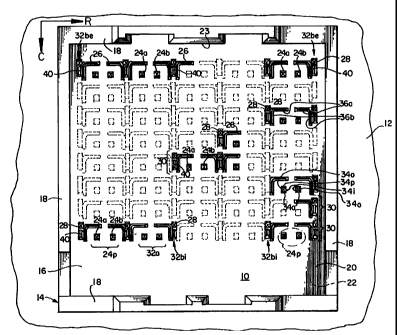
Fig. I is a plan view of a connector side of a header in accordance
with one embodiment of the present invention, and shows such header mounted to
a backplane;
Fig. 2 is a perspective view of a portion of the pins and ground
shields of the header of Fig. 1, with the shroud of Fig. 1 removed for
clarity;
Fig. 3 is the same perspective view of Fig. 2, but shows only the pair
of differential signal pins of FIG. 2;
Fig. 4 is the same perspective view of Fig. 2, but shows only the
ground pins of Fig. 2;
Fig. 5 is the same perspective view of Fig. 2, but shows only the
ground shields of Fig. 2;
Fig. 6 is a perspective view showing a ground pin and a pair of
ground shields in accordance with a second embodiment of the present
invention;
FIG. 7 is a perspective view similar to that of Fig. 2, but from a
different angle, and shows a third embodiment of the present invention which
is
similar to the first embodiment as shown in Figs. 1-5, wherein primary and
secondary headers share common pins and sandwich the backplane
therebetween;
CA 02306033 2000-04-18
BERG-2461/C2356 - 5 - PATENT
Fig. 7A is an exploded perspective view showing the primary header,
backplane, and secondary header of Fig. 7; and
Fig. 7B is a perspective view showing a securing contact employed in
connection with the secondary header of Fig. 7.
Detailed Description of Preferred Embodiments
Certain terminology may be used in the following description for
convenience only and is not considered to be limiting. The words "left",
"right", "upper",
and "lower" designate directions in the drawings to which reference is made.
The words
"inwardly" and "outwardly" are further directions toward and away from,
respectively, the
geometric center of the referenced object. The terminology includes the words
above
specifically mentioned, derivatives thereof, and words of similar import.
Referring to the drawings in detail, wherein like numerals are used to
indicate like elements throughout, there is shown in Fig. 1 a header assembly
or header 10
in accordance with one embodiment of the present invention. As seen, the
header 10 is
mounted to a circuit substrate such as a backplane 12 in a position to receive
a
complementary electrical connector (not shown) on a circuit board (not shown)
to be
coupled to the backplane 12 by way of the electrical connector and header 10.
As seen, the header 10 includes an insulating shroud 14 which has a base
16. As should be understood, when the header 10 is mounted to the backplane
12, the base
16 of the shroud 14 of the header 10 is generally parallel to sucli backplane
12. Typically,
although not necessarily, the shroud 14 of the header 10 also has walls 18
that extend away
from the base 16 at generally right angles thereto. Accordingly, the walls 18
form a well
within which the electrical connector is inserted while mating to the header
10. Typically,
the walls 18 align and guide the electrical connector as it is being inserted
so as to ensure a
proper connection and so as to prevent damage that may occur from mis-
alignment. The
walls 18 may include one or more keying elements (the slots shown, for
example) that
mate to corresponding keying elements in the electrical connector to further
ensure a
proper connection and for polarization.
As should be understood, and as seen in Fig. 1, the base 16 of the shroud 14
has a connector side 20 that faces toward the mating connector, and a
backplane side 22
CA 02306033 2000-04-18
BERG-2461/C2356 - 6 - PATENT
that faces toward the backplane 12. The base 16 of the shroud 14 also has a
primary edge
23, which as will be explained below is designated as such for purposes of
being a fixed
reference in the present disclosure. As seen in Fig. 1, the primary edge 23
runs along the
top qf the base 16.
Header 10 includes signal contacts, ground contacts, and ground shields. In
a differential pair application such as that shown in Fig. 1, the header 10
has a plurality of
pairs 24p of differential signal pins 24a, 24b, a plurality of ground shields
26, and a
plurality of ground pins 28. As should be understood, for purposes of clarity,
only a few
of the elements 24a, 24b, 24p, 26 and 28 are shown in detail, while the
remainder of such
elements are shown in phantom. As seen, each pair 24p of signal pins 24a, 24b,
each
ground shield 26, and each ground pin 28 is mounted to the base 16 of the
shroud 14.
Each signal pin 24a, 24b and each ground pin 28 extends away from the base 16
from both
the connector side 20 and the backplane side 22 in opposing directions
generally
perpendicular to such base 16, as can be seen in and/or appreciated from Figs.
1-4.
As can be seen in Fig. 1, the pairs 24p of signal pins 24a, 24b are arranged
into a plurality of rows 30 extending in a first direction (as indicated by
the arrow R) along
the base 16 and along the primary edge 23 of the base 16. That is to say, the
rows 30 and
the first direction run along the surface of the base 16, and generally
parallel to the primary
edge 23. Additionally, the pairs 24p of signal pin 24a, 24b are further
arranged into a
plurality of colunms 32a that extend in a second direction (as indicated by
the arrow C)
along the base 16 generally perpendicular to the first direction. '.'Again,
that is to say, the
columns 32a and the second direction run along the surface of the base 16, and
generally
perpendicular to the primary edge 23. To summarize, then, the pairs 24p of
signal pins
24a, 24b are arranged generally rectilinearly.
Still referring to Fig. 1, the signal pins 24a, 24b in each pair 24p are
adjacently arranged into a sub-row that extends in the first direction (arrow
R).
Accordingly, each row 30 has X pairs 24p of signal pin 24a, 24b and 2X
individual signal
pins 24a, 24b. Correspondingly, each column 32 has Y pairs 24p of signal pins
24a, 24b,
and 2Y individual signal pins 24a, 24b.
As seen in Figs. 1-3, each signal pin 24a, 24b in a pair 24p has an inner side
34i that faces toward the other signal pin 24a, 24b in the pair 24p, an outer
side 34o
1
CA 02306033 2000-04-18
BERG-2461/C2356 - 7 - PATENT
opposite the inner side 34i, a primary side 34p that extends between the inner
side 34i and
the outer side 34o and that faces toward the primary edge 23 of the base 16,
and a non-
primary side 34a that extends between the inner side 34i and the outer side
34o and that
faces away from the primary edge 23 of the base 16.
Each signal pin 24a, 24b (and each ground pin 28 as well) as shown in the
drawings is generally rectilinear in transverse cross-section, and accordingly
the sides 34i,
34o, 34p, 34a of each signal pin 24a, 24b (and the sides of each ground pin
26) are
generally flat as shown. However, it will be appreciated that the signal pins
24a, 24b (and
the ground pins 26) can have other configurations in transverse cross-section,
including
but not limited to circular, oblong, and multi-sides other than four.
Nevertheless, the sides
34i, 34o, 34p, 34a of each signal pin 24a, 24b as designated above are still
applicable even
if such sides do not correspond to flat surfaces in transverse cross-section.
Although the present invention is described in terms of pairs 24p of
differential signal pins 24a, 24b, it will be recognized that other
arrangements or types of
signal pins may be employed without departing from the spirit and scope of the
present
invention. For example, and depending on the particular application, the
signal pins may
be individually grouped (in a single-ended arrangement), or may be grouped
into threes,
fours, fives, etc.
Referring now to Figs. 1, 2, and 5, in the embodiment of the present
invention shown, at least one ground shield 26 is associated with each signal
pin 24a, 24b.
Preferably, each ground shield 26 generally extends through the,base 16
between the
connector side 20 and the backplane side 22, and more preferably from about
the surface
of the connector side 20 to about the surface of the backplane side 22.
Accordingly, each
ground shield 26 preferably has a depth that generally corresponds to a
thickness of the
base 16 of the shroud 14. As a result, though not shown in Figs. 2-5, it
should be apparent
where the base 16 of the shroud 14 is positioned in relation to the signal
pins 24a, 24b,
ground shields 26, and ground pins 28.
Preferably, each ground shield is generally L-shaped and includes first and
second attached wings 36a, 36b that are arranged at about right angles with
respect to each
other. The first wing 36a of each ground shield 26 may extend generally along
the first
~
direction (arrow R) adjacent and along the primary side 34p or the non-primary
side 34a of
CA 02306033 2000-04-18
- ''--J
BERG-2461/C2356 - 8 - PATENT
the associated signal pin 24a, 24b. Of course, to achieve shielding of each
pair 24p of
signal pins 24a, 24b, it is necessary that some order be provided with regard
to which side
(primary 34p or non-primary 34a) each first wing 36a extends. As but one
example, each
ground shield 26 associated with a signal pin 24a (to the left in Fig. 1) may
extend along
the primary side 34p thereof, and each ground shield 26 associated with a
signal pin 24b
(to the right in Fig. 1) may extend along the non-primary side 34a thereof.
Preferably, the first wings 36a of all the ground shields 26 extend adjacent
and along one or the other of the primary side 34p and the non-primary side
34i of the
respective associated signal pins 24a, 24b. As shown, the first wings 36a of
all the ground
shields 26 extend adjacent and along the primary side 34p of the respective
associated
signal pins 24a, 24b. However, and as was discussed above, in certain
circumstances an
alternate arrangement may be useful.
As seen in Figs. 1, 2, and 5, the second wing 36b of each ground shield 26
generally extends along the second direction (arrow C) adjacent and along the
outside 34o
of the associated signal pin 24a, 24b. With the plurality of ground shields 26
thus arranged
with respect to the pairs 24p of signal pins 24a, 24b, then, and as best
understood by
viewing Fig. 1, the plurality of ground shields 26 in combination
substantially
electromagnetically isolate within the base 16 of the shroud 14 each pair 24p
of signal pins
24a, 24b from every other pair 24p of signal pin 24a, 24b.
Preferably, for each pair 24p of signal pins 24a, 24b, the first wings 36a of
the associated ground shields 26 extend toward each other and ieside generally
in a single
plane. Preferably, such first wings 36a do not actually contact each other,
and the distal
end of each second wing 36b does not extend so far as to directly contact
another ground
shield 26. Accordingly, portions of the material forming the base 16 separate
the ground
shields 26 from one another, and in doing so provide structurally integrity to
such base 16.
Due to the lack of direct connections between ground shields 26, and as can be
appreciated
from Figs. 1, 2, and 5, unshielded gaps exist between the ground shields. Such
gaps
should be minimized so that the pairs 24p of signal pins 24a, 24b are
adequately shielded.
As shown in Fig. 1, except for the pairs 24p in the bottom-most row 30,
each pair 24p of signal pins 24a, 24b is substantially surrounded on all sides
by ground
~
shields 26. In particular, the outer sides 34o and primary sides 34p of the
signal pins 24a,
CA 02306033 2000-04-18
BERG-2461/C2356 - 9 - PATENT
24b are substantially surrounded by the first and second wings 36a, 36b of the
associated
ground shields 26, and the non-primary sides 34a of the signal pins 24a, 24b
are
surrounded by the ground shields 26 associated with the pair 24p of signal pin
24a, 24b
imrnediately below. Since differential pairing is used, shielding between each
signal pin
24a, 24b in each pair 24p is not believed to be necessary. If a single-ended
arrangement is
used, however, shielding between each row of signals may be used. The pairs
24p of
signal pin 24a, 24b in the bottom-most row do not have shielding in the
direction of the
non-primary sides 34a. However, no other signal pins 24a, 24b are in the
immediate
vicinity in such un-shielded direction to create noise and/or cross-talk in
the pairs 24p of
signal pin 24a, 24b in the bottom-most row.
Preferably, and as can be seen from Figs. 1, 2, and 5, each ground shield 26
is generally identical to every other ground shield 26. Moreover, each ground
shield 26 is
symmetrical such that it can be placed adjacent a signal pin 24a or 24b.
Accordingly, only
one type of such ground shield 26 is necessary in constructing the header 10
of the first
embodiment of the present invention. As best seen in Figs. 2 and 5, each
ground shield 26
is of a relatively simple design and in fact may be stamped from an
appropriate sheet of
conductive material into a final form by known forming and/or stamping
processes.
Alternatively, each shield 26 may be molded or extruded by known processes.
Preferably, the shroud 14 of the header 10 is molded from a suitable
insulative material such as a high temperature plastic into a final form by
known
processes, where such final form includes defined apertures foreach signal pin
24a, 24b,
each ground shield 26, and each ground pin 28. Also preferably, each ground
shield 26 is
inserted into the base 16 of the shroud 14 from either the connector side or
backplane side
22, preferably by mechanical means, and such ground shield 26 maintains an
interference
fit with such base 16 of such shroud 14. Preferably, the first or second wing
36a, 36b (the
first wing 36a in Figs. 2 and 5) of each ground shield 26 includes a bump 38a
at a surface
thereof to assist in maintaining the aforementioned interference fit of the
ground shield 26
with the base 16 of the shroud 14.
Alternatively, each signal pin 24a, 24b, each ground shield 26, and/or each
ground pin 28 may be over-molded in situ during formation of the base 16 and
shroud 14.
CA 02306033 2000-04-18
BERG-2461/C2356 -10- PATENT
However, it is presently believed that such in situ over-molding may be
excessively
complicated when compared to other available manufacturing techniques.
Preferably, each ground pin 28 electrically contacts at least one ground
shield 26 at the second wing 36b thereof. More preferably, and as shown in
Figs. 1 and 2,
such contact occurs at the outer surface (the surface away from the associated
signal pin
24a, 24b) of such second wing 36b. Preferably, every ground shield 26
electrically
contacts a ground pin 28. Presumably, at some location, either in the
complementary
electrical connector, the mother board, or in another circuit, each ground pin
28 is
electrically grounded. Accordingly, the ground shields 26 electrically
contacted by the
ground pins 28 are also grounded and are electrically coupled to one another.
Although
described up to now as rigid bumps 38a, 38b, other types of retention features
may be
employed without departing from the spirit and scope of the present invention.
For
example, one or both wings 36a, 36b in each ground shield 26 could include a
compliant
section (not shown) to retain such ground shield 26 in the base 16 of the
shroud 14 and/or
to retain an associated ground pin 28 in such base 16 of such shroud 14.
Preferably, and as best seen in Figs. 2 and 4, each ground pin 28 includes a
generally planar fin 40 that generally resides within the base 16 of the
shroud 14 and that
extends generally laterally from the main body of the ground pin 28. As seen
in Fig. 1, the
fin 40 extends generally in the second direction (arrow C), and has generally
opposing
planar sides 42 (Figs. 2, 4). Accordingly, each ground shield 26 is
electrically contacted
by a ground pin 28 at a planar side 42 of the fin 40 of such grouhd pin 28.
Preferably, the ground pins 28 are arranged into a plurality of rows 30 that
extend in the first direction (arrow R), and a plurality of columns 32be, 32bi
that extend in
the second direction (arrow C). As seen in Fig. 1, each row 30 of ground pins
28
corresponds to a row 30 of signal pin 24a, 24b, and each column 32be, 32bi of
ground pins
28 alternates with a column 32a of pairs 24p of signal pins 24a, 24b. As seen,
columns
32be of ground pins 28 are a pair of exterior or outer-most columns (left and
right) and
columns 32 bi of ground pins 28 are at least one interior column (four are
sho'A,-n in Fig. 1)
positioned between such exterior columns 32be. Preferably, each ground pin 28
in each
interior column 32bi is positioned between and electrically contacts first and
second
ground shields 26 on either lateral side of such ground pin 28. As will be
described below,
CA 02306033 2000-04-18
BERG-2461/C2356 -11- PATENT
each ground pin 28 in each interior column 32bi preferably contacts bumps 38b
on wings
36b of such first and second ground shields 26. Also preferably, each ground
pin 28 in'
each exterior column 32be is positioned adjacent and electrically contacts
only a single
ground shield 26 on one lateral side thereof.
In the case of a ground pin 28 in one of the interior columns 32bi, it is seen
from Fig. 1 that the first ground shield 26 corresponding to such ground pin
28 is
associated with a signal pin 24a, 24b of a first pair 24p of signal pins on
one side of the
ground pin 28 (the left side, for example), the second ground shield 26 is
associated with a
signal pin 24a, 24b of a second pair 24p of signal pin 24a, 24b on the other
side of the
ground pin 28 (the right side, to continue the example), and the first and
second ground
shields 26 electrically contact the ground pin 28 at either planar side of the
fin 40 thereof.
As seen, then, the first and second pairs 24p of signal pins 24a, 24b both
reside in a row 30
that corresponds to the row 30 of the ground pin 28 at issue; more precisely,
such ground
pin 28 and such first and second pairs 24p of signal pin 24a, 24b can be
considered to
reside in a single row 30 (although not necessarily linearly aligned within
the row 30). As
also seen, such first and second pairs 24p of signal pins 24a, 24b
respectively reside in
immediately adjacent columns 32a on either side of the column 32bi of the
ground pin 28
at issue.
In the case of a ground pin 28 in one of the exterior columns 32be, it is also
seen from Fig. 1 that the single ground shield 26 corresponding to such ground
pin 28 is
associated with a signal pin 24a, 24b of a single pair 24p of sigtial pins on
one side of such
ground pin 28, and the single ground shield 26 electrically contacts the
ground pin 28 at
one planar side of the fin 40 thereof. Similar to the previous case, the
single pair 24p of
signal pins 24a, 24b resides in a row 30 corresponding to the row 30 of such
ground pin
28. In this case, the single pair 24p of signal pins 24a, 24b resides in an
immediately
adjacent column 32a on only one side of the column 32be of such ground pin 28.
In either case, each ground pin 28 is preferably inserted into the base 16 of
the shroud 14 from either the connector side or backplane side 20, 22 thereof,
as with the
ground shields 26. Such operation may be performed by appropriate automatic
insertion
machinery. Preferably, each ground pin 28 in the interior columns 32bi
maintains an
interference fit between contacted second wings 36b of the first and second
ground shields
CA 02306033 2000-04-18
BERG-2461/C2356 -12- PATENT
26, and more preferably between contacted bumps 38b on such second wings 36b.
Correspondingly, it is preferable that each ground pin 28 in the exterior
columns 32be
interference fits between the contacted second wing 36b of the single ground
shield 26 and
with an interior surface of the base 16 (not shown) where such interior
surface is opposite
the contacted second wing 36b of the single ground shield 26. Preferably, and
as best seen
in Figs. 2 and 5, each second wing 36b of each ground shield 26 includes a
bump or bumps
38b at a contact surface thereof (the outer surface as shown in Figs. 1, 2,
and 5) to assist in
electrically contacting the ground pin 28 at the fin 40 thereof, and to assist
in maintaining
the aforementioned interference fit.
As with the ground pins 28 and ground shields 26, each signal pin 24a, 24b
is preferably inserted into the base 16 of the shroud 14 from either the
connector side or
backplane side 20, 22 thereof, and preferably maintains an interference fit
with such base
16. Such insertion operation may be performed by appropriate automatic
insertion
machinery. More preferably, all of the aforementioned elements are inserted
into the base
16 of the shroud 14 from the backplane side 22. As should be understood, the
backplane
side 22 is more readily accessible since it is not obstructed by any walls 18.
Moreover,
insertion from the backplane side 22 locks pins 24a, 24b, 28 in place upon
securing the
header 10 to the backplane 12. Preferably, and as seen in Figs. 2 through 4,
each signal
pin 24a, 24b and each ground pin 28 preferably includes various contact
surfaces that
assist in maintaining an interference fit directly with the base 16 of the
shroud 14.
Preferably, each signal pin 24a, 24b and each grdund pin 28 includes a
compliant section 44 exterior from the base 16 adjacent the backplane side 22
thereof, as
best seen in Figs. 2-4. As should be understood, each compliant section 44
maintains an
interference fit with plated through holes in the backplane 12 when the header
10 is
mounted thereto. As should be appreciated, it is undesirable to insert the
compliant
sections 44 into the base 16 of the shroud 14. Such compliant portions 44 may
deform or
likely would not easily fit through such base 16 during such insertion.
In one embodiment of the present invention, and referring again to Fig. 1,
each signal pin 24a, 24b and each ground pin 28 in transverse cross-section is
approximately 0.4 mm by 0.4 mm in width and height, in the region of the main
pin
portions that are received by the complementary electrical connector.
Additionally, in
-
CA 02306033 2000-04-18
~- ~
BERG-2461/C2356 -13 - PATENT
such embodiment, each ground shield 26 has a main thickness of about 0.2 mm.
Accordingly, if each signal pin 24a, 24b and each ground pin 28 in a row 30 is
spaced
about 1.0 mm in the first direction (arrow R), each signal pin 24a, 24b may be
separated
from its corresponding ground shield 26 by about 0.4 mm. Such distance is
sufficient to
provide a reasonable degree of structural integrity to the base 16 of the
shroud 14.
Referring now, to Fig. 6, it is seen that in a second embodiment of the
present invention, each ground pin 28' does not have the fin 40 of the ground
piii 28 (Figs.
2 and 4), and each ground shield 26' does not have the contacting bump(s) 38b
of the
ground shield 26 (Figs. 2 and 5). Instead, each ground shield 26' includes an
integral tab
46 that contacts a contact portion 48 of the ground pin 28', where the contact
portion 48 is
generally in-line with respect to the longitudinally extending ground pin 28'.
Preferably,
the tab 46 is formed within the ground shield 26' by an appropriate stamping
or molding
operation, and the tab 46 is inclined slightly away from the main body of the
ground shield
26' and toward the ground pin 28'. Accordingly, the tab 46 is urged into good
electrical
contact with the contact portion 48 when the ground pin 28' and the ground
shield 26' are
mounted to the base 16 of the shroud 14 (not shown in Fig. 6). As shown, the
ground pin
28' is for an interior column 32bi since two ground shields 26' flank such
ground pin 28'.
Of course, only one ground shield 26' would flank the ground pin 28' if such
ground pin
28' were in an exterior column 32be.
Referring now to Fig. 7, it is seen that in a third embodiment of the present
invention which is similar to the first embodiment as shown in Pigs. 1-5, a
primary header
l0a has pairs 24p of signal pins 24a, 24b and ground pins 28 that extend a
relatively longer
distance (as compared with the header 10 of Figs. 1-5) beyond the backplane 12
than the
header 10 shown in Figs. 1-5. In addition, a secondary header lOb is
positioned on the
other side of the backplane 12 and generally opposite the primary header l0a
such that the
secondary header lOb receives and includes the extended portions of the pairs
24p of
signal pins 24a, 24b. Accordingly, the backplane 12 is sandwiched between the
primary
and secondary headers 10a, l Ob, each header 10a, lOb shares the pairs 24p of
signal pins
24a, 24b and the ground pins 28, and a circuit board mounted to the primary
header l0a is
directly interfaced through the backplane 12 to another circuit board mounted
to the
secondary header l Ob. Each header 10a, 10b has its own ground shields 26 (the
ground
CA 02306033 2000-04-18
BERG-2461/C2356 -14- PATENT
shields 26 for the primary header 10a are not shown in Fig. 7). Unlike the
primary header
10a, the secondary header l Ob includes a plurality of securing contacts 50,
where each
securing contact 50 electrically contacts a respective ground pin 28 and
secures such
ground pin 28 to such header lOb. As seen, each securing contact 50 also
electrically
contacts at least one ground shield 26 within the secondary header l Ob
through bumps
38b, thereby electrically connecting the contacted ground shield(s) 26 with
the contacted
ground pin 28.
In particular, the primary header l0a of Fig. 7 is substantially identical to
the header 10 of Figs. 1-5, except that the pairs 24p of signal pins 24a, 24b
and ground
pins 28 extend a relatively longer distance as compared with the header 10 of
Figs. 1-5 to
allow for rear plug-up. For example, in the header 10 of Figs. 1-5, such pins
24a, 24b, 28
extend about 4.3 mm through and beyond the backplane 12, while in the primary
header
l0a of Fig. 7, such pins 24a, 24b, 28 extend about 19 mm through and beyond
the
backplane 12.
Preferably, each pin 24a, 24b, 28 is formed such that the distal end thereof
(i.e., the end associated with the secondary header lOb) is substantially
identical to the
proximal end thereof (i.e., the end associated with the primary header l0a).
Accordingly,
the secondary header l Ob is instantiated by way of a second shroud 14
substantially
identical to the shroud 14 of the primary header 10a, where the second shroud
14 is slipped
over the distal end of each pin 24a, 24b, 28 (Fig. 7A) after such pins are
inserted through
the backplane 12. As should be understood, the second shroud.'14 is then moved
toward
the backplane 12 until the base 16 of such second shroud 14 is generally
parallel to and in
contact with such backplane 12. As viewed from their respective connector
sides 20, then,
the primary header l0a and the secondary header l Ob each present
substantially the same
profile, pin arrangement, and 'footprint'. In fact, it is preferable that the
primary header
l0a and the secondary header 10b each be able to receive the same type of
complementary
electrical connector in their respective wells. Preferably, the primary edge
23 of the
secondary header 10b is directly opposite the primary edge 23 of the primary
header 10a,
with respect to the backplane 12.
As was discussed above, and as similarly shown in Figs. 2 and 4, each
~round pin 28 in the primary headerl0a includes a generally planar fin 40 that
generally
CA 02306033 2000-04-18
. .... -.~
BERG-2461/C2356 -15- PATENT
resides within the base 16 of the shroud 14 of the primary header l0a and that
extends
generally laterally from the main body of the ground pin 28. As seen, each fin
40 has
generally opposing planar sides such that each ground shield 26 in the primary
header l0a
is electrically contacted by a ground pin 28 at a planar side of the fin 40 of
such ground pin
28. As was also discussed above, each ground pin 28 is preferably inserted
into the shroud
14 of the primary header l0a such that the fin 40 maintains an interference
fit therewith.
However, and as should be understood, the insertion of each ground pin 28
through the backplane 12 prevents such ground pin 28 from having a second fin
on the
distal end thereof. Accordingly, and as was discussed above, it is preferable
that the
secondary header lOb include a plurality of securing contacts 50, where each
securing
contact 50 contacts a respective ground pin 28, secures such ground pin 28 to
such header
l Ob, electrically connects such ground pin 28 to at least one ground shield
26 (through
bumps 38b), and in effect performs the same function as a fin 40.
In particular, it is preferable that, prior to being mounted to the backplane
12 and the pins 24a, 24b, 28, the second shroud 14 be fitted with a plurality
of conductive
securing contacts 50, where one contact 50 is in each space in the base 16 of
the second
shroud 14 where a second fin of a ground pin 28 would otherwise reside. The
insertion of
contacts 50 is generally similar to the insertion of shields 26 into the base
16. As seen in
Fig. 7B, each such securing contact 50 has generally opposing planar sides,
and as
positioned in the second shroud 14 of the secondary header l Ob is
electrically contacted on
at least one side by a ground shield 26 in the secondary header 1'Oa at a
planar side of such
securing contact 50.
When the second shroud 14 is slipped over the distal end of each pin 24a,
24b, 28 and moved toward the backplane 12, then, each securing contact 50 in
such second
shroud 14 securingly electrically contacts the side of a respective ground pin
28 and
maintains an interference fit therewith. Preferably, each securing contact 50
includes a
compliant or spring portion 52 in facing relation to the side of the
respective ground pin 28
to assist in securingly electrically contacting the respective ground pin 28
and maintaining
the interference fit therewith. As with the fin 40, each securing contact 50
engages bumps
38b on the contacted-to ground shields 26. However, any other appropriate
mechanism
CA 02306033 2000-04-18
~. _ .~
BERG-2461/C2356 -16- PATENT
may be employed to perform such functions without departing from the spirit
and scope of
the present invention.
With such securing contacts 50, the ground shields 26 in the second shroud
14 are electrically coupled to the ground pins 28. In addition, the entire
second shroud 14
is secured to the backplane 12. The interference fit between the securing
contacts 50 and
the ground pins 28 secures the second shroud 14 to the backplane 12.
In the foregoing description, it can be seen that the present invention
comprises a new and useful header 10 for being mounted to a circuit substrate
such as a
backplane 12. The header 10 can have multiple differential signal pairs 24p in
relatively
high density, and ground shields 26 for each pair 24p such that each pair 24p
of signal pins
24a, 24b is shielded from every other pair 24p of signal pins 24a, 24b by such
ground
shields 26. Moreover, the header is practical and relatively easily
manufactured. It should
be appreciated by those skilled in the art that changes could be made to the
embodiments
described above without departing from the inventive concepts thereof. It is
understood,
therefore, that this invention is not limited to the particular embodiments
disclosed, but it
is intended to cover modifications within the spirit and scope of the present
invention as
defined by the appended claims.