Note: Descriptions are shown in the official language in which they were submitted.
CA 02306111 2000-03-27
WO 99/21288 PGT/US98/21658
1
PCM MODEM EQUALIZER WITH ADAPTIVE COMPENSATION FOR ROBBED BIT
SIGNALLING
BACKGROUND OF THE INVENTION
1. Field of the Invention
The present invention relates broadly to the field of
telecommunications. More particularly, the present invention
relates to a modem equalizer for a PCM modem Where the modem
equalizer will function properly in the presence of a robbed-bit
signalling network.
2. State of the Art
With the ever-increasing importance of telecommunications
for the transfer of data as well as voice, there has been a
strong effort to increase data transfer rates over the telephone
wires. Recently, the ITU-T adopted the V.34 Recommendation
(International Telecommunication Union, Telecommunication
Standardization Sector Recommendation V.34, Geneva, Switzerland
1994) which is hereby incorporated by reference herein in its
entirety. The V.34 standard and subsequent amendments define
modem operating speeds of 28.8 kbps up to 33.6 kbps, and the
vast majority of modems being sold today adhere to the V.34
Recommendation. However, with the explosion in the use of the
Internet, even at the V.34 transfer rates, downloading of large
files available on the Internet can take long periods of time.
Thus, recently, there has been a thrust to provide additional
standards recommendations which will increase data transfer
rates even further (note the TIA TR-30.1 PCM Modem ad hoc group
and the ITU-T Study Group 16).
Recognizing that further increases in data rates is
theoretically limited (see C.E. Shannon, "A Mathematical Theory
of Communication," Bell System Technical Journal, 27:379-423,
623-656 (1948)), there have been various proposals to take
advantage of the fact that much of the telecommunication network
is now digital. For example, U.S. Patent No. 5,394,437 to
Ayanoglu et al., U.S. Patent No. 5,406,583 to Dagdeviren, and
CA 02306111 2000-03-27
WO 99/21288 PGT/US98I21658
2
U.S. Patent No. 5,528,625 to Ayanoglu et al. (all assigned to
AT&T/Lucent and' all of which are hereby incorporated by
reference herein in their entireties) all discuss techniques
which utilize the recognition that the network is mostly digital
in order to increase data transmission rates to 56 kbps and
higher. Similarly, Kalet et al., "The Capacity of PAM Voiceband
Channels," TFFF International Conference on Communications '93,
pages 507-511 Geneva, Switzerland (1993) discusses such a system
where the transmitting end selects precise analog levels and
timing such that the analog to digital conversion which occurs
in the central office may be achieved with no quantization
error. PCT application number PCT/US95/15924 (Publication WO
96/18261) to Townshend (which is hereby incorporated by
reference herein in its entirety) discusses similar techniques.
All of the disclosures assume the use of PAM (pulse amplitude
modulation) digital encoding technology rather than the QAM
(quadrature amplitude modulation) currently used in the V.34
Recommendation. The primary difference between the AT&T
technology and the Townshend reference is that the AT&T
technology suggests exploiting the digital aspect of the
telephone network in both "upstream" and "downstream"
directions, while Townshend appears to be concerned with the
downstream direction only. Thus, systems such as the "x2"
technology of US Robotics which are ostensibly based on
Townshend envision the use of the V.34 Recommendation technology
for upstream communications. As will be appreciated by those
skilled in the art, the technologies underlying the V.34
Recommendation, and the proposed 56 kbps modem are complex and
typically require the use of high-end digital signal processors
(DSPs) .
One of the tasks of the modem is the task of equalizing
incoming signals. Equalization is a technique used to
compensate for distortion in analog signal lines. One of the
distortions which is compensated for is Intersymbol Interference
(ISI) which is described in more detail below. Prior to data
communication, two communicating modems engage in a training
sequence wherein the equalizers of the modem receivers are set
CA 02306111 2000-03-27
WO 99/21288 PCT/US98/21658
3
to compensate for the quality of the analog signal line which
links the modems. However, it has been found that training of
the equalizer in the modem receiver is adversely affected if the
connection between the receiving modem and the ultimate source
of the received data includes both analog and digital signal
lines. In particular, training is adversely affected by robbed
bit signaling (RBS) introduced by the digital network into the
digital data stream and by Digital Pad Attenuation (DPA) in the
digital network.
RBS is a technique used in T1 network connections where the
least significant bit of each nth data octet is replaced with a
control bit by the network for control signalling. The
frequency of robbed bits through a single T1 connection is one
every sixth symbol. This "in-band" signalling is used to
indicate things like "off-hook", "on-hook", "ringing", "busy
signal", etc. RBS results in data impairment by changing
transmitted bit values. When the data flowing through the
network is digitized audio voice signals, a change in the least
significant bit of some octets will introduce noise or
distortion into the ultimate analog audio reproduction of the
digitized voice signal. Nevertheless, this has been found to be
acceptable for voice communications. When the data flowing
through the network is digital data, however, RBS can have very
serious consequences. For this reason, when data is sent
through a T1 network connection, the least significant bit of
each octet is often not used and the data is sent as seven bit
symbols. This mitigates the RBS problem if the link between the
two data units is completely digital, at the expense of reducing
bandwidth of the link by one eighth. Since a T1 line carries
twenty four 64k channels, if one 64k channel is used in a
combined analog/digital link to a modem, conventional methods of
eliminating RBS (i.e., using seven-bit symbols) would limit the
maximum theoretical bandwidth of the connection to 56k. This
theoretical maximum would never be reached because of the
presence of ISI and DPAs. Thus, the problem of RBS is a major
obstacle to exploiting the maximum possible bandwidth of the
combined analog and digital link; and if one wishes to exploit
CA 02306111 2000-03-27
WO 99/21288 PCT/US98/21658
4
the entire bandwidth of the link, one must deal directly with
the RBS problem.
The problem of RBS is even further complicated when the
link between two data units includes several different digital
legs such that the frequency of RBS is variable from one
connection to another. In other words, if the link includes
several different digital legs in which bits are robbed, the
frequency of robbed bits can increase significantly.
During PCM modem training, it is impossible for the
receiver to know whether a symbol has been impaired due to RBS.
As a result, RBS can interfere with the equalizer training
process and result in misadjustment of the equalizer. In turn,
equalizer error will lead to improper and/or inadequate channel
equalization, with the ensuing inability to perform other tasks
such as channel measurements, etc. This will prevent the
receiver from ever making proper compensations for ISI and DPAs.
Prior art Fig. 1, shows a simplified model of data
transmission through a combined analog/digital link. At 11,
binary data is provided in the digital part of the network and
represents data from either an intrinsically binary source or an
appropriately encoded (A-Law or ~,-Law) analog quantity which is
to be transmitted to the desired destination. The digital
channel 13 carries binary data through one or more legs of the
network. For purposes of Fig. 1, the digital channel can be
characterized by the way it affects the binary data it carries
relative to the original binary data presented at 11. The
binary data carried by the digital channel 13 is at some point
subjected to a digital-to-analog converter 15 which maps or
translates binary data into an analog symbol format, such as a
PCM level, suitable for transmission through an analog channel.
The D/A conversion takes place at the rate of 1/T Hz, where T
seconds is the duration of the symbol interval.
The analog signal is then provided to an analog channel 17
which carries the analog waveforms to a PCM modem 19. Due to
CA 02306111 2000-03-27
WO 99lZ1288 PCT/US98/2165$
its band-limited nature, the analog channel 17 introduces
distortion or inter-symbol interference (ISI) as well as noise
into the stream of analog waveforms it carries. ISI causes
individual symbols to interact with one another, thereby
distorting the signals.
The PCM modem 19 is coupled to the analog channel 17 and
includes, among other things, a receiver 21 and an analog
channel decoder 23. The receiver 21 receives the analog signals
at its input, and includes means for synchronizing the receiver
with the data source/transmitter. The receiver 21 also includes
an equalizer which compensates for ISI distortion introduced in
the analog channel. The equalized signal may then be translated
by the analog channel decoder 23 and formatted into a binary
data stream which is sent to a further destination 25 (e.g., a
receiving computer).
As previously mentioned, the analog channel 17 introduces
ISI which can significantly distort the signal at the receiver.
Indeed, as a result of ISI, the symbol received at the receiver
21 at time instant kT is no longer determined by the transmitted
symbol alone, but by a linear combination of a (theoretically
possibly infinite) number of previously transmitted symbols.
ISI can be a severe impairment for certain types of analog
channels; especially those with spectral nulls in their
magnitude response at various frequencies such as DC. The ISI
problem of an analog channel is compounded by the fact that its
impulse response is in general unknown. Thus, the ISI affects
data symbols in an unknown way and seriously complicates the
task of the receiver of correctly detecting the incoming symbols
with a low probability of error. Noise added at the output of
the analog channel compounds the difficulty of correcting for
ISI.
Equalization of the signal to account for ISI and noise is
absolutely essential for proper communications. Various
equalizer filter architectures are known for such equalization.
For example, an equalizer called a decision feedback equalizer
CA 02306111 2000-03-27
WO 99/21288 PGTIUS98/Z1658
6
(DFE) which is shown in prior art Fig. 2 is known to be
effective in cases of severe amplitude distortion. As seen in
Fig. 2, the DFE 30 includes a feed-forward finite impulse
response (FIR) equalizer 32, first and second summers 34, 36, a
decision block 38, and a feedback FIR equalizer 40. The feed-
forward FIR provides a feedforward equalized component (Rff) to
the summer 34 which is compared to the feedback equalized
component (Rfb) provided by the feedback FIR 40 to provide an
equalized estimated symbol (R). This estimated symbol (R) is
provided to the decision block 38 as well as to the second
summer 36. The decision block 38 generates a decision based on
the equalized estimated symbol. The decision is fed back to the
input of the feedback FIR equalizer 40, and is also sent to the
second summer 36. The second summer 36 takes the difference
between the estimated symbol and the output symbol, i.e., the
error, and provides the error to the feed-forward FIR 32 and to
the feedback FIR 40 in order to update the equalizer tap
coefficients of the FIRs 32 and 40.
It should be appreciated that in the modem training period
(prior to sending data), a decision block is not used. Rather,
as seen in prior art Fig. 3, the decision block 38 is replaced
with a reference generator 37 which generates a reference
(known) sequence Tk. The reference sequence is compared at the
second summer 36 to the estimated symbol R to provide an error a
which is used as feedback in order to update the equalizer tap
coefficients 31 (Cff) and 39 (Cfb) of the FIRs 32 and 40.
While the adaptive equalizer of Figs. 2 and 3 is effective
in compensating for ISI analog channel impairments, it does not
account for digital channel impairments which can be present in
PCM-type modem communications. In particular, the adaptive
equalizers of the prior art are not effective in the presence of
robbed bit signaling which causes octets in the training
sequence-to be translated into analog symbols which are
different than what they would otherwise be. Similarly, octet
transformation due to digital PAD attenuation is problematic in
causing individual training symbols to be translated into
CA 02306111 2000-03-27
WO 99/21288 PCT/US98/21658
7
different analog levels. The PAD impairment can occur with RBS,
either before or after a bit is robbed.
It has been discovered that RBS, when present, occurs in a
repeating frame of six bytes. Table 1, below, shows an example
of an RBS Frame in which bytes 1, 3, and 4 are affected by RBS.
It should be noted that, as mentioned above, RBS may be present
in conjunction with DPAs and the robbed bit may occur before or
after the pad.
E~____RgS Frame______________~I
0 1 2 3 4 5 0 1 2 3 4 5 0
X X X X X X
Table 1
SUMMARY OF THE INVENTION
It is therefore an object of the invention to provide
methods and apparatus for mitigating the consequences of robbed
bit signaling in a digital stream received by a PCM modem.
It is also an object of the invention to provide adaptive
methods and apparatus for mitigating the consequences of robbed
bit signaling in a digital stream received by a PCM modem.
It is another object of the invention to provide methods
and apparatus for mitigating the consequences of robbed bit
signaling which work in conjunction with conventional adaptive
equalizers.
It is a further object of the invention to provide methods
and apparatus for determining the pattern of RBS, if any, in the
data stream, to remove the influence of RBS on the results of
CA 02306111 2000-03-27
WO 99/21288 PCT/US98/21658
8
equalization, and to permit the adaptive equalizer to achieve
substantially the same quality of channel equalization as when
RBS is absent from the data stream.
In accord with these objects which will be discussed in
detail below, the methods and apparatus of the present invention
include providing an RBS estimator and decision modulator in
conjunction with an adaptive equalizer. In a preferred
embodiment, the adaptive equalizer is a conventional DFE having
first and second summers and feedforward and feedback
equalizers. The RBS estimator and decision modulator receives
the error signals from the second summer in the DFE, receives
either the equalized estimated signals R from the first summer
of the DFE or remodulated symbols T~k, and outputs a gain
correction signal (1+g) which is applied to the output (Tk) of
the reference generator to provide the remodulated symbols
(T~Mk). The remodulated symbols are provided to the feedback
equalizer, to the second summer, and if desired, to the RBS
estimate and decision modulator. The methods of the invention
are based on the recognition that the effects of RBS can be
detected in the amplitude modulation of the main training
sequence stream. The modulation will occur in a periodic
repetitive pattern of length 6*T where T is the symbol interval.
Therefore, the invention applies a corrective gain to the
decision in each time slot in a periodic manner having the same
period 6*T. More particularly, for each time interval Tk over a
period of 6*T, the symbol present at the time interval is
sampled and a respective corrective gain g(6k-j) is applied to
it, where j has the values 0 through 5. The gain applied to
each of the six time slots is adaptively updated over a training
period until each of the six gain coefficients is optimized.
According to a presently preferred embodiment of the
invention, the adaptive decision remodulator calculates gain
according to either:
gj c~+ ~~-; - gl c~-,~+ wj * Rcs~-,~ * ecs~-,~ ( 1 a ) or
~~a+l-W ~c~k-~+~~ * T cst-i~ * ecbk-i~ ( lb)
CA 02306111 2000-03-27
WO 99/Z1288 ' PCT/US98/21658
9
where gj~6~x+1)_~) is a value of the jth decimated remodulation gain
predicted for the time 6 (k+1 ) -j, g j ~6x_ j) is the current value of
the jth decimated remodulation gain for the time 6k-j, ~ij is an
adaptation constant for the jth gain, R~sx_~) is the current value
of the equalized (estimated) symbol, and e~sx_~) is the current
equalization error using the current T~M~6x_ j) . These gain
coefficients are applied sequentially corresponding to repeating
frames of symbols T from the reference generator in order to
generate remodulated values of T and error values e.
The main precondition for the engagement of the adaptive
decision modulator is that the adaptive equalizer has first
reached a certain level of equalization prior to introducing the
adaptive decision modulator into the loop. For the type of
impairments introduced by RBS, the steady state signal-to-noise
ratio (SNR) obtained by the equalizer prior to introducing the
adaptive decision modulator into the loop may be quite low
(e.g., 2ldb). Under these circumstances no further reduction in
MSE (mean squared error) is possible unless the adaptive
decision modulator is introduced into the loop. However, using
the adaptive decision modulator of the invention, the final
equalizer coefficient solution substantially eliminates the
affects of RBS.
Additional objects and advantages of the invention will
become apparent to those skilled in the art upon reference to
the detailed description taken in conjunction with the provided
figures.
BRIEF DESCRIPTION OF THE DRAWINGS
Figure 1 is a schematic flow chart of the downstream flow
of data to a prior art PCM modem from a digital source where the
link between the upstream source and the downstream modem
includes both digital and analog network channels;
Figure 2 is a schematic block diagram of a prior art DFE in
operation after training;
CA 02306111 2000-03-27
WO 99/21288 PCT/US98/Z1658
Figure 3 is a schematic block diagram of a prior art DFE in
operation during training:
Figure 4 is a schematic block diagram of a DFE with RBS
correction according to the invention;
Figure 5 is a schematic block diagram of a periodic gain
generator according to the invention;
Figures 6a and 6b are schematic block diagrams of
alternative embodiments of one branch of an adaptive decision
modulator according to the invention; and
Figure 7 is a schematic block diagram of a generic adaptive
equalizer with RBS correction according to the invention.
DETAILED DESCRIPTION OF THE PREFERRED EMBODIMENTS
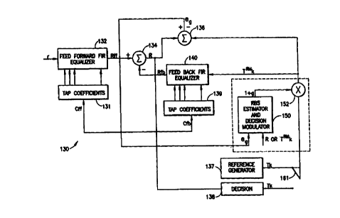
Referring now to Figure 4, a decision feedback equalizer
130 with adaptive decision correction according to the preferred
embodiment of the invention includes some of the components of a
prior art DFE which are indicated with reference numerals
similar to those shown in Figures 2 and 3 but incremented by
100. Thus, the DFE 130 includes a feed-forward finite impulse
response (FIR) equalizer 132, first and second summers 134, 136,
a reference generator 137 and decision block 138, and a feedback
FIR equalizer 140. The feed-forward FIR provides a feedforward
equalized component (Rff) to the summer 134 which is compared to
the feedback equalized component (Rfb) provided by the feedback
FIR 140 to provide an equalized estimated symbol (R). This
estimated symbol (R) is provided to the second summer 136 which
is also coupled (via multiplier 152) to the output of a
reference generator 137 which generates a reference (known)
sequence (Tk). In accord with the invention, periodic gain
coefficients (1+g) are applied at multiplier 152 to the sequence
(Tk) to provide remodulated symbols (T~k) which are fed as a
sequence to the summer 136. These remodulated symbols (TRMk) are
also fed to the feedback FIR 140. The remodulated reference
CA 02306111 2000-03-27
WO 99/21288 PG"f/US98/21658
11
sequence (T~k) is compared at the second summer 136 to the
estimated symbol (R) to provide an error (eg) which is used as
feedback in order to update the equalizer tap coefficients 131
(Cff) and 139 (Cfb) of the FIRs 132 and 140. According to the
invention, the error (eg) is also used as an input to the RBS
estimator and decision modulator 150 (which also receives an
input (R) from summer 134 or an input T~Mk from multiplier 152).
Once the training has been accomplished, instead of
utilizing the reference generator 137 to provide the sequence
Tk, a decision block 138 is used to generate the sequence Tk.
Thus, switch 161 is used to switch from the reference generator
137 to the decision block 138. The decision block 138 utilizes
the.equalized estimated symbol (R) in making its decision as is
well known in the art.
In order to better understand the basic operations of the
RBS estimator and decision modulator 150, the periodic
application of gain gj(k) to symbols Tk to obtain remodulated
symbols T~k can be illustrated as a synchronously rotating
commutator as shown in Figure 5. The commutator diagram shown
in Figure 5 shows three synchronously rotating switches 160,
162, 164 each of which has six positions j=5,4,3,2,1,0, each
position referring to a time slot in the 6*T period of an
unknown RBS pattern. As illustrated in Figure 5, all of the
switches are at the position j=5 when the incoming stream of
training symbols Tk is at the start of a six symbol RBS pattern
or frame. Thus, the symbol sampled at switch 160 when it is in
the first position j=5 is labelled T(6k-5). The gain
coefficient applied to this symbol is selected at switch 162
which is synchronously at the same j=5 position. The gain
coefficient at this position is labelled [1+g5(6k-5)] and
represents the gain coefficient which will be repeatedly applied
to each T(6k-5). Switch 164 represents the remodulated symbols
T~k, each of which is calculated by multiplying the respective
symbol Tj(k) by the respective gain coefficient gj(k). It will
therefore be understood that the RBS estimator and decision
modulator 150 will generate a repeating pattern of six gain
CA 02306111 2000-03-27
WO 99!21288 PCT/US98/21658
12
coefficients which are synchronized with the stream of training
symbols in order to adjust the amplitude of the locally
generated training symbols to match the RBS-altered amplitude of
the symbols in the received signal stream R. When the locally
generated training symbols are so remodulated, the DFE is
permitted to correctly adjust the tap coefficients by comparing
the estimated signal R with the remodulated reference signal T~k
which has now been adjusted to compensate for the effects of RBS
on the estimated signal R. Therefore, the tap coefficients for
the symbols which have been affected by RBS are set differently
than they would have been set were it not for the remodulation
of the locally generated training symbols.
The decision modulator 150, according to the invention,
operates adaptively to estimate the RBS pattern and assign the
appropriate gain coefficients to each slot in the repeating RBS
frame. As mentioned above, according to a presently preferred
embodiment of the invention, the adaptive decision remodulator
calculates gain according to
~j~~+1~-~- ~j~~-~+ ~,j * R~~_~ * e~~_~ ( la) or
g) ~p~+ iri - $1 ask-n'~' N~j * T c~k-i> * ec6k-i~ ( lb )
where g j ~6 ~x+i>-j~ is a value of the jth decimated remodulation gain
predicted for the time 6(k+1)-j, gj~sx_~~ is the current value of
the jth decimated remodulation gain for the time 6k-j, ~.j is an
adaptation constant for the jth gain, R~6x_~~ is the current value
of the equalized (estimated) symbol, and a ~sx_~~ is the current
decision error using the current T~M~sx_~~ . The adaptation
constant ~.j is appropriately chosen as is known in the art.
These gain coefficients are applied iteratively to repeating
frames of symbols Tk from the reference generator in order to
generate remodulated values of T~k according to
T~ _~=Tc~_~, * (i + ~(6k-j)l
(2)
CA 02306111 2000-03-27
WO 99/Z1288 PGT/US98/21658
13
Each time a symbol Tk is remodulated, a new error a is generated
at the second summer 136 in Figure 4 according to
e~s~-~= R<6t -p-T<6t-» ( 3 )
Each error a is used in equation (1) above to recalculate the
gain coefficients for each jth slot in the RBS frame. The
interaction of the equations (1a) or (lb) through (3) is shown
diagrammatically in Figures 6a and 6b which represent the
application of the equations to each jth slot in the RBS frame.
Turning now to Figure 6a, according to a first embodiment,
the gain (g) for the jth slot of the RBS frame is added to "1" at
170a to provide a gain coefficient which is multiplied by the
current training symbol (T) at 172a to produce a remodulated
training symbol (T~) Which is subtracted from the equalized
symbol (R) at 174a. The "summing" (which takes place at the
summer 136 in Figure 4) produces the decision error (e) which is
used to calculate the predicted gain for the next iteration of
the jth slot of the RBS frame. The error (e) is multiplied by
the symbol (R) at 176a and this product is multiplied by the
adaptation constant (~.) for this jth slot at 178a. The product
created at 178a is then added to the present gain (g) at 180a to
produce the gain for the next occurrence of this jth slot in the
RBS frame at 182a. The accumulated set of six gains is stored
at a buffer 184a (such as a FIFO) which produces the current
gain for summation at 170a and 180a based on the last predicted
gain which is provided at 182a.
Turning to Fig. 6b, in an alternative preferred embodiment,
the gain (g) for the jth slot of the RBS frame is added to "1" at
170b to provide a gain coefficient which is multiplied by the
current training symbol (T) at 172b to produce a remodulated
training symbol (TAM) which is subtracted from the equalized
symbol (R) at 174b. The "summing" (which takes place at the
summer 136 in Figure 4) produces the decision error (e) which is
used to calculate the predicted gain for the next iteration of
the jth slot of the RBS frame. The error (e) is multiplied by
CA 02306111 2000-03-27
WO 99/21288 PCT/US98/21658
14
the remodulated symbol (T~sk_j) at 176b and this product is
multiplied by the adaptation constant (fit) for this jth slot at
178b. The product created at 178b is then added to the present
gain (g) at 180b to produce the gain for the next occurrence of
this j~'' slot in the RBS frame at 182b. The accumulated set of
six gains is stored at a buffer 184b (such as a FIFO) which
produces the current gain for summation at 170b and 180b based
on the last predicted gain which is provided at 182b.
It will be appreciated that when the decision modulator is
initialized, there are no gain values available for application
to the summer 170a or 170b. According to the presently
preferred embodiment of the invention, the buffer 184a or 184b
is initially filled with six zeros. It will also be appreciated
that the operations shown in Figure 6 are carried out
independently for each of the six slots (j=1, 2, 3, 4, 5, 0) in
the RBS frame. It will further be appreciated that these
operations are carried out for k=n iterations of the RBS frame
until the stream of symbols (R) has been adequately equalized.
It will be understood that each slot j in the repeating frame
may have a different gain coefficient. From frame to frame,
however, the repeating gain coefficient applied to each
particular slot j should become relatively constant. Thus,
after iteratively adjusting slot gains for n frames, the system
should equalize with a constant repeating pattern of gain
coefficients which may then be applied to the output of the
decision block.
It should be appreciated that the main precondition for the
engagement of the adaptive decision modulator is that the
equalizer has first reached a certain level of equalization
prior to introducing the adaptive decision modulator into the
loop (i.e., another switch, not shown, may be provided and used
to bypass the RBS estimator and decision modulator). For the
type of impairments introduced by RBS, the steady state signal-
to-noise ratio (SNR) obtained by the DFE prior to introducing
the adaptive decision modulator into the loop may be quite low
(e.g., 2ldb). Under these circumstances no further reduction in
CA 02306111 2000-03-27
WO 99lZ1Z88 PCT/LJS98/21658
MSE (mean squared error) is possible unless the adaptive
decision modulator is introduced into the loop. However, using
the adaptive decision modulator of the invention, the final
equalizer coefficient solution substantially eliminates the
affects of RBS.
Turning to Fig. 7, the PCM modem equalizer of the invention
is shown using a more generic "adaptive equalizer" 301 instead
of a DFE. In Fig. 7, components which are similar to those
shown in Figures 4 are incremented by 100. Thus, incoming
signals are received by the adaptive equalizer 201 which outputs
an equalized estimated symbol (R). The estimated symbol R is
fed to a decision block 238, to a summer 236, and, according to
one embodiment, to the RBS estimator and decision modulator 250.
From the estimated symbol R, the decision block 238 generates a
sequence of output decisions Tk (it being appreciated that
during training, instead of the decision block 238 being
utilized, a reference generator is utilized to provide Tk). The
output decisions Tk are multiplied by the output (1+g) of the
RBS estimator and decision modulator 250 to provide remodulated
symbols T~Mk. Differences between the remodulated symbols (T~Mk)
and the estimated symbols (R) are taken at the summation block
236 to generate error values (eg), and the error values are fed
back to the adaptive equalizer 201 and the RBS estimator and
decision modulator 250. As can be seen from Fig. 7 (as well as
Figs. 9-6), the RBS estimator and decision modulator 250
utilizes the error values (eg) as well as either the estimated
symbols (R) or the remodulated symbols T~Mk in generating a gain
(g)
There have been described and illustrated herein a PCM
modem equalizer with adaptive compensation for robbed bit
signalling. While particular embodiments of the invention have
been described, it is not intended that the invention be limited
thereto, as it is intended that the invention be as broad in
scope as the art will allow and that the specification be read
likewise. Thus, while the invention has been described as being
typically implemented in a DSP of the modem, it will be
CA 02306111 2000-03-27
wo 99n1288 PCT/US98n1658
16
appreciated that different hardware and/or software can be
utilized. Indeed, the invention can be implemented as part of a
soft-modem". Also, while particular block diagrams were
provided, it will be appreciated that the invention can be
implemented using different equivalent blocks. Thus, instead of
a 6*T FIFO buffer, other types of buffers could be utilized. In
fact, in certain circumstances, different buffers will be
required. -For example, in certain circumstances, particulars of
the network cause an asymmetry in the translation of positive
levels and negative levels. Where this asymmetry is present,
separate positive and negative corrective gains must be
determined for each of the six slots, thereby requiring
effectively twelve gain adjustments (g) to be determined. Thus,
the buffer must be capable of storing twelve values and being
accessed upon demand, depending upon whether a positive or
negative gain adjustment is required for the particular incoming
value. Similarly, in certain networks, the value of the robbed
bit in even numbered RBS frames is not equal to the value of the
robbed bit in odd numbered frames. In this case, corrective
gains must be assigned separately to even and odd numbered
frames, thereby requiring effectively twelve gain adjustments to
be determined. Of course, where the network has both the
asymmetry and the changing robbed bit values present, twenty-
four corrective gain adjustments must be determined and stored.
It will therefore be appreciated by those skilled in the art
that yet other modifications could be made to the provided
invention without deviating from its spirit and scope as so
claimed.