Note: Descriptions are shown in the official language in which they were submitted.
CA 02306126 2000-04-13
WO 99/19717 PCT/US98I21869
LAMINATE MICROSTRUCTURE DEVICE
AND METHOD FOR MAKING SAME
BACKGROUND
This invention relates to methods and apparatus for high throughput sample
analysis.
In a range of technology-based industries, including the chemical, bioscience,
biomedical, and pharmaceutical industries, it has become increasingly
desirable to develop
capabilities for rapidly and reliably carrying out chemical and biochemical
reactions in large
numbers using small quantities of samples and reagents. Carrying out a massive
screening
program manually, for example, can be exceedingly time consuming and may be
entirely
impracticable where only a very small quantity of an important sample or
component of
interest is available, or where a component of a synthesis or analysis is very
costly.
Developments in a variety of fields have resulted in an enormous increase in
the
numbers of targets and compounds that can be subjected to screening.
Rapid and widespread advances in the scientific understanding of critical
cellular
processes, for example, has led to rationally designed approaches in drug
discovery. Molecular
genetics and recombinant DNA technologies have made possible the isolation of
many genes,
and the proteins encoded by some of these show promise as targets for new
drugs. Once a
target is identified and the gene is cloned, the recombinant protein can be
produced in a
suitable expression system. Often receptors and enzymes exist in alternative
forms, subtypes or
isoforms, and using a cloned target focuses the primary screen on the subtype
appropriate for
the disease. Agonists or antagonists can be identified and their selectivity
can then be tested
against the other known subtypes. The availability of such cloned genes and
corresponding
expression systems require screening methods that are specific, sensitive, and
capable of
automated very high throughput.
Similarly, an emergence of methods for highly parallel chemical synthesis has
increased
the need for high throughput screening ("HTS"). Conventionally, preparation of
synthetic
analogs to the prototypic lead compound was the established method for drug
discovery.
Natural products were usually isolated from soil microbes and cultured under a
wide variety of
conditions. The spectrum of organisms employed by the pharmaceutical industry
for isolation
of natural products has now expanded from actinomycetes and fungi to include
plants, marine
organisms, and insects. More recently, the chemistry of creating combinatorial
libraries has
vastly increased the number of synthetic compounds available for testing.
Thousands to tens or
hundreds of thousands of small molecules can be rapidly and economically
synthesized. See,
CA 02306126 2000-04-13
WO 99/19717 PCTNS98/21869
-2-
e.g., U.S. Patent No. 5,252,743 for a discussion of combinatorial chemistry.
Thus,.
combinatorial libraries complement the large numbers of synthetic compounds
available from
the more traditional drug discovery programs based, in part, on identifying
lead compounds
through natural product screening.
Accordingly, considerable resources have been directed to developing methods
for
high-throughput chemical syntheses, screening, and analyses. A considerable
art has emerged,
in part from such efforts.
Competitive binding assays, originally developed for immunodiagnostic
applications,
continue to be commonly employed for quantitatively characterizing receptor-
ligand
interactions. Despite advances in the development of spectrophotometric- and
fluorometric-
based bioanalytical assays, radiolabeled ligands are still commonly employed
in pharmaceutical
HTS applications. Although non-isotopic markers promise to be environmentally
cleaner,
safer, less expensive, and generally easier to use than radioactive compounds,
sensitivity
limitations have prevented these new methods from becoming widespread. Another
major
disadvantage of the competition assay is the number of steps, most notably
washing steps,
required to run assays.
Scintillation proximity assays, discussed for example in U.S. Patent No.
4,271,139 and
U.S. Patent No. 4,382,074, were developed as a means of circumventing the wash
steps
required in the above heterogeneous assays. The homogeneous assay technology,
which
requires no separation of bound from free ligand, is based on the coating of
scintillant beads
with an acceptor molecule such as, for example, the target receptor.
in another approach to avoiding the use of radioactive labels, especially
useful in high-
throughput assays, lanthanide chelates are used in time-resolved fluorometry.
See, e.g., U.S.
Patent No. 5,637,509. '
Automated laboratory workstations have contributed significantly to advances
in
pharmaceutical drug discovery and genomic science. See, e.g., U.S. Patent No.
5,104,621 and
U.S. Patent No. 5,356,525. Particularly, robotics technology has played a
major role in
providing practical means for carrying out HTS methods. See, e.g., U.S. Patent
No.
4,965,049.
Robotio-based high-throughput tools are now routinely used for screening
libraries of
compounds for the purpose of identifying lead molecules for their therapeutic
potential. For
example, a screening method for characterising ligand binding to a given
target employing a
CA 02306126 2000-04-13
WO 99/19717 PCT/US98/21869
-3
variety of separation techniques is described in WO 97/01755, and a related
method is
described in U.S. Patent No. 5,585,277.
I~ghly parallel and automated methods for DNA synthesis and sequencing have
also
contributed significantly to the success of the human genome project, and a
competitive
industry has developed. Examples of automated DNA analysis and synthesis
include, e.g., U.S.
Patent No. 5,455,008; U.S. Patent No. 5,589,330; U.S. Patent No. 5,599,695;
U.S. Patent
No. 5,631,734; and U.S. Patent No. 5,202,231.
Computerized data handling and analysis systems have also emerged with the
commercial availability of high-throughput instrumentation for numerous life
sciences research
and development applications. Commercial software, including database and data
management
software, has become routine in order to efficiently handle the large amount
of data being
generated.
With the developments outlined above in molecular and cellular biology,
combined with
advancements in combinatorial chemistry, there has been a huge increase in the
number of
targets and compounds available for screening. In addition, many new human
genes and their
expressed proteins are being identified by the human genome project and will
therefore greatly
expand the pool of new targets for dnrg discovery. A great need exists for the
development of
more efi"lcient ultrahigh throughput methods and instrumentation for
pharmaceutical and
genomic science screening applications.
Miniaturization of chemical analysis systems, employing semiconductor
processing
methods, including photolithography and other wafer fabrication techniques
borrowed from
the microelectronics industry, has attracted increasing attention and has
progressed rapidly.
The so-called "lab-on-a-chip" technology enables sample preparation and
analysis to be carried
out on-board microfluidic-based cassettes. Moving fluids through a network of
interconnecting
enclosed microchannels of capillary dimensions is possible using
electrokinetic transport
methods.
Applications of microfluidics technology embodied in the form of analytical
devices has
many attractive features for pharmaceutical high throughput screening.
Advantages of
miniaturization include greatly increased throughput and reduced costs, in
addition to low
consumption of both samples and reagents and system portability.
Implementation of these
developments in microfluidics and laboratory automation hold great promise for
contributing
to advancements in life sciences research and development.
CA 02306126 2000-04-13
WO 99/19717 ~- PCT/US98/21869
Of particular interest are microfluidics devices in which very small volumes
of fluids are
manipulated in microstructures, including microcavities and microchannels of
capillary
dimension, at least in part by application of electrical fields to induce
electrokinetic flow of
materials within the microstructures. Application of an electric potential
between electrodes
contacting liquid media contained within a microchannel having cross-sectional
dimensions in
the range from about 1 pm to upwards of about 1 mm results in movement of the
contents
within the channel by electroosmotic flow and/or by electrophoresis.
Electrophoresis is
movement of electrically charged particles, aggregates, molecules or ions in
the liquid medium
toward or away from the electrodes. Electroosmotic flow is bulk fluid flow,
including
movement of the liquid medium and of dissolved or suspended materials in the
liquid medium.
The extent of bulk fluid flow resulting from application of a given electrical
field depends
among other factors upon the viscosity of the medium and on the electrical
charge on the wall
of the microchannel. Both electroosmotic flow and electrophoresis can be used
to transport
substances from one point. to another within microchannel device.
Electrophoresis has become an indispensable analytical tool of the
biotechnology and
other industries, as it is used extensively in a variety of applications,
including separation,
identification and preparation of pure samples of nucleic acids, proteins, and
carbohydrates;
identification of a particular analyte in a complex mixture; and the like. Of
increasing interest in
the broader field of electrophoresis is capillary electrophoresis ("CE"),
where particular
entities or species are moved through a medium in an electrophoretic chamber
of capillary
dimensions under the influence of an applied electric field. Benefits of CE
include rapid run
times, high separation efficiency, small sample volumes, etc. Although CE was
originally
carried out in capillary tubes, of increasing interest is the practice of
using microchannels or
trenches of capillary dimension on a planar substrate, known as microchannel
electrophoresis
("MCE"). CE and MCE are increasingly finding use in a number of different
applications in
both basic research and industrial processes, including analytical,
biomedical, pharmaceutical,
environmental, molecular, biological, food and clinical applications.
Typically, the microchanneis of MCE devices are constructed by forming troughs
or
grooves of appropriate dimension and configuration in one surface of a planar
rectangular- or
disc-shaped base substrate, and applying a planar cover to the surface to
enclose the
microchannels.
CA 02306126 2000-04-13
WO 99/19717 -5- PCT/US98/21869
Conventionally, microchannels having capillary dimensions have been made in
silicon or
glass substrates by micromachining, or by employing photolithographic
techniques. See, e.g.,
U.S. Pat. No. 4,908,112, U.S. Pat. No. 5,250,263. Where the substrates are of
fused silica, the
microchannels can be enclosed by anodic bonding of a base and a cover.
Exemplary MCE
devices are also described in U.S. 5,126,022; U.S. 5,296,114; U.S. 5,180,480;
and
U.S. 5,132,012; and in Harrison et al., "ll~cromachining a Miniaturized
Capillary
Electrophoresis-Based Chemical Analysis System on a Chip," Science (1992) 261:
895;
Jacobsen et al., "Precolumn Reactions with Electrophoretic Analysis Integrated
on a
Microchip," Anal. Chem. (1994) 66: 2949; Effenhauser et al., "High-Speed
Separation of
Antisense Oligonucleotides on a Micromachined Capillary Electrophoresis
Device," Anal.
Chein. {1994) 66:2949; and Woolley & Mathies, "Ultra-High-Speed DNA Fragment
Separations Using Capillary Array Electrophoresis Chips," P.N.A.S. USA (1994)
91: I 1348.
Eckstrom et al. U.S. Pat. No. 5,376,252 describes a process for creating
capillary size
channels in plastic using elastomeric spacing layers. t5hman International
Patent Publication
WO 94129400 describes a method for producing microchannel structures by
applying a thin
layer of a thermoplastic material to one or both of the surfaces to be joined,
then joining the
surfaces and heating the joined parts to melt the thermoplastic bonding layer.
Kaltenbach et al.
U.S. Pat. No. 5,500,071 describes constructing a miniaturized planar
microcolumn liquid
phase analytical device by laser ablating microstructures in the surface of a
planar laser
ablatable polymeric or ceramic substrate, rather than by conventional silicon
micromachining
or etching techniques.
U.S. Patent Application Serial No. 08/878,437 filed June 18, 1997 (Attorney
Docket
No. A-63519/RFTBK SOAN 011) describes methods for fabricating microchannel
structures
constructed of a polymeric card-shaped or diso-shaped base plate having a
planar surface in-
which a microchannel structure is formed, and a planar polymeric cover. The
microchannel
structure is enclosed by bonding the planar surfaces of the cover and the base
plate together.
SUMMARY OF THE INVENTION
In one general aspect, the invention features a continuous form microstructure
(i.e.,
microcavity and/or microchannel) array device constructed as an elongate
flexible film laminate
containing a plurality of microstructures or arrays of microstructures
arranged serially
lengthwise along the laminate. Where the device has a series of
microstructures, each structure
CA 02306126 2000-04-13
WO 99/19717 PCT/US98I21869
-6-
is configured to carry out a fluidic process or a step in a fluidic process.
Where the device has
a series of microchannel arrays, each array is configured to carry out a set
of processes or
steps, on an array of samples or of test reagents.
Because the microstructures, or arrays of microstructures, are serially
arranged
lengthwise along the laminate, the device can be fed lengthwise into and
through an analytical
device, and the structures or arrays can be treated serially in a continuous
automated or
semiautomated manner.
In some embodiments the flexible elongate laminate device is advanced within
the
analytic device from a continuous uncut supply roll, through the various parts
of the analytical
device and, as the laminate device is expended, to a takeup roll, similar to
the way in which roll
film is advanced frame-by-frame through a camera. In other embodiments the
elongate
laminate device is advanced within the analytic device from a continuous uncut
accordion-
folded supply stack, through the analytical device and, as the laminate device
is expended, to
an accordion-folded takeup stack. When the entire roll (or supply stack) has
been expended
and passed onto the takeup roll (or stack), the expended roll (or stack) can
be discarded, or
can conveniently and efficiently be stored in an archive, as may be desirable
for some uses.
The microstructures are constructed either by forming channels, trenches or
cavities of
suitable dimension and configuration in a microchannel surface of a first
lamina and, optionally,
enclosing the channels by apposing a covering surface of a second lamina onto
the
microchannel surface to form the microstructures; by forming slits having
suitable dimension
and configuration in a spacing lamina, and sandwiching the spacing lamina
between first and
second enclosing laminae to enclose the slits between the apposed surfaces of
the first and
second enclosing laminae to form the microchannels or by combining a spacing
lamina having
slits therein with a lamina having such channels, trenches or cavities formed
therein.
Electrodes can be formed in the device by any of a variety of techniques,
known in the
art, including application of wires or conductive decals, or printing or
stamping using
conductive inks, or vapor deposition, etc., in a specific configuration onto a
surface of one or
both of the laminae. The laminate construction according to the invention is
particularly
suitable for application of flexible printed circuit technology. For technical
review, See,
Th. H. Stearns (1996), Flexible Printed Circuitry, SMTnet Bookstore. See also,
U.S. 4,626,462; U.S. 4,675,786; U.S. 4,715,928; U.S. 4,812,213; U.S.
5,219,640;
U.S. 5,615,088.
CA 02306126 2000-04-13
WO 99/19717 PCT/US98/21869
Processes for making flexible printed circuits are generally well known.
Briefly, the
electrodes, which provide connections from the reservoirs in the microfluidic
structure to high-
voltage contacts in an analytical device that carried the laminate, are formed
within a thin
polymer film laminate, which serves as a cover lamina to be afl'lxed as
described above to the
base lamina, as described in more detail below.
In this context, an "analytical device" is a device that includes at least a
detector capable
of detecting or of measuring a signal produced in the course of the
microfluidic process or
process step, and means for moving the laminate in relation to the analytical
device to bring a
detection region in the microstructure within the field of the detector.
Usually the analytical
device is in a stable installation, and the laminate is advanced through it
past the detector, but
in some embodiments the laminate is held in place and the analytical device is
moved along it.
Of course, any number of such detectors may be employed, each alignable with a
detection
region (or series of detection regions, as the laminate progresses through).
Usually, the
analytical device also includes electrical contacts each alignable with a
contact point in
electrical circuitry employed to generate electroflow in the microstructure.
Each such contact
is electrically connected to a source of electrical power, and to control
means (which may be
automated) for changing the applied electric fields as the microfluidic
process proceeds. The
analytical device may further include means for adding various fluids (e.g.,
samples, buffers or
other solvents, reagents, and the like) to the microstructures by way of
access ports in the
laminate. The analytical device may additionally include means for changing
the environmental
conditions surrounding a portion of the laminate, such as temperature, and the
like.
In some embodiments, the device is provided as an assembled laminate, in which
the
microchannels are fully enclosed; and in which ports or reservoirs are
provided for
introduction of sample or reagents or test compounds or liquid media; and in
which electrodes
have been emplaced and provided with leads for connection to a source of
electrical power.
Reagents, samples, test compounds, and/or media can be introduced as
appropriate during or
just prior to conducting the assays. In some embodiments the assembled
laminate is provided
with at least some of the media or reagents "on board" in the microchannels or
reservoirs as
appropriate. Where the device is provided with one or more substances already
on board, the
device can additionally be provided with means for protection of degradable
contents from
variations in ambient conditions and, particularly, for example, a release
liner which resists loss
CA 02306126 2000-04-13
WO 99/19717 PCT/US98/21869
-g
of moisture or of volatile contents and/or which resists light exposure to the
contents, may be
provided as a release liner on one or both surfaces of the laminate.
The device and method of the invention provides a full range of advantages in
analytical
sensitivity that inhere in the use of conventional microfluidic analysis,
while at the same time.
providing for automated or semiautomated continuous processing of high numbers
of analyses
at high rates of speed. The complexity of mass screening programs, for
example, is
substantially reduced by elimination of many of the manipulation steps,
whether by hand or by
machine, that are required in use of conventional assay plates. And
possibilities for error are
reduced by reduction of the number of points at which manipulation by hand is
required.
Methods and apparatus according to the invention for carrying out multiple
microfluidic
manipulations at high throughput rates are readily adaptable for automated non-
contact
dispensing of reagents or samples, providing for substantially reduced risk of
cross-
contamination.
Further, the continuous form assay array according to the invention
significantly
reduces the bulk volume of disposable materials, as compared with conventional
assay card
methods, both because the flexible laminates themselves are thinner than are
conventional
assay cards, and because the microchannel structures or arrays can be arranged
on the
continuous form device with more eiI'lcient use of the substrate surface area.
BRIEF DESCRIPTION OF THE DRAWINGS
Fig. lA is a diagrammatic sketch showing a portion of an embodiment of the
laminate
construction of a continuous form microchannel device of the invention.
Fig. 1B is a diagrammatic sketch of the portion of the embodiment of Fig. 1 A,
in an
exploded view, showing the laminae.
Fig. 2A is a diagrammatic sketch of a portion of an alternate embodiment of
the
laminate construction of a continuous form microchannel device of the
invention.
Fig. 2B is a diagrammatic sketch of the portion of the embodiment of Fig. 2A,
in an
exploded view, showing the laminae.
Figs. 3A, 3B are diagrammatic sketches in plan view of two alternative
embodiments of
microchannel structures configured as standard injection crosses, in which the
separation
channel is curved (Fig. 3A) or folded (Fig. 3B) to provide extended separation
flow path
length.
CA 02306126 2000-04-13
WO 99/19717 _9_ PCTIUS98/Z1869
Fig. 3C is a diagrammatic sketch in plan view of an embodiment of a
microchannel
structure providing for introduction of four reagents into a sample flow path
upstream from
the separation channel, which is folded to provide extended separation flow
path length.
Fig. 4 is a diagrammatic sketch in plan view of a portion of the length of an
embodiment
of a continuous form microchannel device of the invention, showing two in a
series of
microchannel arrays.
Fig. 5 is a diagrammatic sketch in a perspective view showing a method for
constructing an elongate flexible film laminate having the general laminate
structure shown in
Fig. lA.
Fig. 6 is a diagrammatic sketch in a side view showing a method for
constructing an
elongate flexible film laminate having the general laminate structure shown in
Fig. 2A.
Figs. 7a, b are diagrammatic sketches in sectional view showing details of an
embodiment of a device according to the invention made using a flexible
circuit iamina.
Figs. 8a, b are diagrammatic sketches as in Figs. 7a, b showing details of an
alternative
embodiment of a device according to the invention made using a flexible
circuit lamina.
Fig. 9 is a diagrammatic sketch showing a microstructure configuration that
can be
constructed in a continuous form laminate device of the invention, suitable
for carrying out a
receptor binding assay.
Fig. 10 is a diagrammatic sketch showing a microstructure configuration that
can be
constructed in a continuous form laminate device of the invention, suitable
for carrying out an
enzyme assay.
Fig. l la is a diagrammatic sketch of a portion of the length of an embodiment
of a base
lamina of a continuous form microstructure device of the invention, showing
two in a series of
microchannel arrays. Each microchannel array includes four microstructures
each configured
to carry out a receptor binding assay, as described with reference to Fig. 9.
Fig. l lb is a diagrammatic sketch of a portion of the length of flexible
circuit laminate
showing two in a series of layouts of electrodes and electrical contacts, each
layout configured
to serve a microchannel array as shown in Fig. 11 a.
Fig. 11 c is a diagrammatic sketch of a portion of the length of an embodiment
of a
continuous form elongate laminate microstructure device of the invention,
constructed by
laminating the flexible circuit laminate ofFig. l lb onto the base lamina
ofFig. l la.
CA 02306126 2000-04-13
WO 99/19717 -10- PCT/US98/21869
Fig. 12 is an isometric view of a laminate microstnrcture device of the
present invention
and a contact probe assembly for use therewith.
Fig. 13 is a cross-sectional view of the laminate microstructure device of
Fig. 12 taken
along the line 13-13 of Fig. 12 with another embodiment of a contact probe
assembly for use
therewith.
Fig. 14 is a cross-sectional view similar to Fig. 13 of another embodiment of
a laminate
microstructure device of the present invention and another embodiment of a
contact probe
assembly for use therewith.
Fig. 15 is a plan view of a further embodiment of a laminate microstructure
device of
the present invention.
Fig. 16 is a cross-sectional view of the laminate microstructure device of
Fig. 15 taken
along the line 16-16 of Fig. 15.
Fig. 17 is a cross-sectional view similar to Fig. 13 of yet another embodiment
of a
laminate microstructure device of the present invention and an contact) probe
for use
therewith.
Fig. 18 is a top plan view, partially cut away, of another embodiment of a
laminate
microstructure device of the present invention.
Fig. 19 is a cross-sectional view of the laminate microstructure of Fig. 18
taken along
the line of 19-19 ofFig. 18.
The drawings are diagrammatic only and not to scale and, particularly, in some
of the
Figs. the thicknesses of the laminate composites and of the layers of which
they are
constructed are much exaggerated for clarity of presentation.
DETAILED DESCRIPTION - -
jn General
"Microfluidic processing", as that term is used herein, means and refers to
fluid
processing-that is, fluid handling, transport and manipulation-carried out
within chambers
and channels of capillary dimension. Valueless sample injection is achieved by
moving fluid
from reagent reservoirs into cross-channel injection zones, where plugs of
buffer or test
compounds are precisely metered and dispensed into a desired flowpath. The
rate and timing
of movement of the fluids in the various microchannels can be controlled by
electrokinetic,
CA 02306126 2000-04-13
WO 99/19717 -11- PCT/US98/21869
magnetic, pneumatic, and/or thermal-gradient driven transport, among others.
These sample-
manipulation methods enable the profile and volume of the fluid plug to be
controlled over a
range of sizes with high reproducibility. In addition, microfluidic processing
includes sample
preparation and isolation where enrichment microchannels containing separation
media are
employed for target capture and purification. Microfluidic processing also
includes reagent
mixing, reactionrncubation, separations and sample detection and analyses.
Generally, the expression "microstructure", as used herein, means and refers
to a single
enclosed microchannel or a network of interconnecting microchannels having
cross-sectional
dimensions suitable for carrying out microfluidic manipulations of materials
carried by them.
Several steps or stages of an analytical process may be carried out in one
microchanneI
structure, suitably configured. Configurations of various complexity are
disclosed for example
in U.S. Patent Application Ser. No. 08/902,855 filed July 30, 1997 [Attorney
Docket No. A-
62855-I/RFT'BK SOAN-8-1] and in U.S. Patent Application Ser. No. 081878,447
filed June
18, 1997 [A-64739/RFTBK SOAN-017], the entire contents of each of which are
incorporated herein by this reference.
A "microfluidic network", as that term is used herein, is a system of
interconnected
microchannels, i.e., cavity structures and capillary-size channels, through
which fluids can be
manipulated and processed.
Cavity structures, in the context of microstructures, are spaces, usually
formed in, e.g.,
a planar substrate, a plate, or the like in accordance with the present
invention. Cavity
structures include, e.g., wells, reservoirs, chambers for incubation or
separation or detection,
and the like. Cavity structures can be present at one or both of the termini,
i.e., either end, of a
channel, and are there usually referred to as reservoirs. Such cavities
structures may serve a
variety of purposes, such as, for example, means for introducing a buffer
solution, elution r
solvent, reagent rinse and wash solutions, and so forth into a main channel or
one or more
interconnected auxiliary channels, receiving waste fluid from the main
channel, and the like. In
some embodiments, cavity structures are not connected by channels, but rather
stand alone;
such free standing cavities can be used for reagent introduction, on-board
mixing, incubation,
reactions, detection and the like. In another embodiment, these individual
steps of a
homogeneous assay can be carried out in a cavity.
In the microstructures of the invention "channels", usually "microchannels",
provide
conduits or means of communication (usually fluid communication and more
particularly liquid
CA 02306126 2000-04-13
WO 99/19717 -12- PCT/US98/21869
communication), between cavity structures and the like. Channels include
capillaries, grooves,
trenches, microflumes, and so forth. The channels may be straight, curved,
serpentine,
labyrinth-like or other convenient configuration within the planar substrate.
The cross-
sectional shape of the channel may be circular, ellipsoidal, trapezoidal,
square, rectangular,
triangular and the like within the planar substrate in which it is present.
The inside of the channel may be coated with a material to improve the
strength of the
microstructure, for modifying, enhancing or reducing etectroosmotic flow, for
enhancing or
reducing etectrophoretic flow, for modification of surface
hydrophobicity/hydrophilicity, for
binding of selected compounds, and so forth. Exemplary coatings are
silylation, polyacrylamine
(vinyl-bound), methylcellulose, polyether, polyvinylpyrrotidone, and
polyethylene glycol,
polypropylene, Teflon'~'"r (DuPont), NafionT"~ (DuPont), polystyrene sulfonate
and the like may
also be used. See also U.S. Patent Application Serial No. 08/715,338, the
relevant disclosure
of which is incorporated herein by reference.
A "microchannel", as that tenor is used herein, is an at least partly enclosed
trench or
channel or cavity having capillary dimensions, that is, having cross-sectional
dimensions that
provide for capillary flow along the channel. Usually at least one of the
cross-sectional
dimensions, e.g., width, height, diameter, is at least about 1 pm, usually at
least 10 pm; and is
usually no more than 500 pm, preferably no more than 200 pm. Channels of
capillary
dimension typically have an inside bore diameter ("B7") of from about 10 to
200 microns,
more typically from about 25 to 100 microns.
Microchannels can provide for electroflow between cavity structures and the
like in the
microstructures of the invention. "Electroflow", as used herein, is the
manipulation of entities
such as molecules, particles, cells, vitreous fluid and the like through a
medium under the
influence of an applied electric field by use of electrodes and the like to
induce movement such
as electrokinetic flow, electroosmotic flow, electrophoretic flow,
dielectrophoretic flow, and
so forth. Depending upon the nature of the entities, e.g., whether or not they
carry an electrical
charge, as well as upon the surface chemistry of the chamber in which the
electroflow is
conducted, the entities may be moved through the medium under the direct
influence of the
applied electric field or as a result of bulk fluid flow through the pathway
resulting from the
application of the electric field, e.g., eiectroosmotic flow. It is within the
purview of the
present invention that electroflow can be carried out in conjunction with
movement of material
by other means than application of an electric field, such as by gravity or by
application of a
CA 02306126 2000-04-13
WO 99/19717 -13- PCTIUS98121869
magnetic field, centrifugal force, thermal gradients, aspiration, negative
pressure, pumping,
pneumatic forces, and the like.
An "electroflow medium" is an electrically conductive medium, that is
generally utilized
in carrying out microfluidic processes. The particular medium chosen is one
that is suitable to a
particular application of the present invention. Such media include, for
example, buffer
solutions, cross-linked and uncross-linked polymeric solutions, organic
solvents, detergents,
surfactant micellular dispersions, gels of the type generally used in
connection with analytical
separation techniques and other microfluidic processes, and so forth. For
example, cross-
linked polyacryIamide gel, cellulose derivatives, uncross-linked
polyacrylamide and derivatives
thereof, polyvinyl alcohols, polyethylene oxides and the like may be used. For
a discussion of
such media see, e.g., Barron and Blanch, "DNA Separations by Slab Gel and
Capillary
Electrophoresis: Theory and Practice", Separation and Purification Methods
{/995) 24:1-118.
Suitable electroflow media include conventional buffers such as, for example,
the
Good's buffers (HEPES, MOPS, MES, Tricine, etc.), and other organic buffers
(Tris, acetate,
citrate, and formate), including standard inorganic compounds (phosphate,
borate, etc.).
Exemplary buffer systems include: (i) 100 mM sodium phosphate, pH 7.2; (ii)
89.5 mM tris-
base, 89:5 mM Boric acid, 2 mM ETDA, pH 8.3. Buffer additives include:
methanol, metal
ions, urea, surfactants, and zwitterions, intercalating dyes and other
labeling reagents.
Polymers can be added to create a sieving buffer for the differential
separation of molecular
species, such as, e.g., nucleic acids, proteins, and the like, based on
molecular size. Examples
of such polymers are: polyacrylamide (cross-linked or linear), agarose,
methylcellulose and
derivatives, dextrans, and polyethylene glycol. Inert polymers can be added to
the separation
buffer to stabilize the separation matrix against factors such as convective
mixing.
Alternatively, buffers containing micelles can be used for effecting
separation of r
electrically neutral or hydrophobic substances of interest. The micelles are
formed in the buffer
by addition of an appropriate surfactant at a concentration exceeding the
critical micelle
concentration of that detergent. Useful surfactants include but are not
limited to sodium
dodecyl sulfate, dodecyltrimethyl ammonium bromide, eic. Weakly charged or
apolar analytes
partition into the micelles to different degrees depending upon their degree
of hydrophobicity
and thus can be separated. This subtechnique of capillary electrophoresis is
termed micellar
electrokinetic chromatography.
CA 02306126 2000-04-13
WO 99/19717 -14- PGT/US98/21869
"Electrophoresis" is separation of components in a liquid by electroflow.
Various forms
of electrophoresis include, by way of example and not limitation, free zone
electrophoresis, gel
electrophoresis, isotachophoresis, high performance CE, capillary zone
electrophoresis, and
the like. In the context of the microstructures according to the invention, an
"electrophoresis
column" is a channel for carrying out electrophoresis.
A microstructure can be made by forming one or more trenches or channels or.
cavities
in the desired configuration and with the desired dimensions in one surface of
a lamina, and
then optionally covering selected portions at least of the trenches or
channels or cavities with a
second lamina to form one or more enclosed microchannels. Or, a microstructure
can be made
by forming slits in the desired configuration and with the desired dimensions
through a spacing
lamina having a desired thickness, and then enclosing selected portions at
least of the slits by
sandwiching the spacing lamina between two enclosing laminae to form one or
more enclosed
microchannels.
As noted above, the enclosed volumes within the microchannels provide "flow
paths",
in which the various components of the analytical process can move and combine
and interact
or react, and in which analytes can be separated electrophoretically or
retained by capture
media. Any of a variety of means can be employed to provide sources of supply
of the various
components to the flow paths.
Any of a variety of means can be employed to cause movement of the various
components within the microchannels. Usually, as noted above, an electric
field is applied to a
segment of a microchannel to cause electrokinetic transport (by electroosmotic
flow or by
electrophoresis, or by some combination of EOF and electrophoresis) of the
contents of the
microchannel segment. An electric field can be applied by positioning a pair
of electrodes,
connected to a source of electrical power, within the microchannel at the ends
of the
microchannel segment. Where it is desired, for example, to move a buffer from
a buffer
reservoir along a microchannel to a buffer waste reservoir, the pair of
electrodes can be
positioned so that they contact the fluid within the respective reservoirs;
application of an
electric potential across the electrodes induces a electrokinetic flow from
one reservoir to the
other through the microchannel.
Additionally, as noted above, other means than electrokinetic flow may be used
to move
the components within the microchannels, and, particularly, to fill the
microchannel structure
CA 02306126 2000-04-13
WO 99/19717 PCTNS98I21869
-15-
at the outset, or to introduce an aliquot of sample material or of a test
compound, for example,
at the beginning of or in the course of the analysis.
As used herein, the expression "array of microchannel structures" means and
refers to a
set of microchannel structures, typically but not necessarily alt having the
same or similar
configurations, each operating to carry out one of a set of related analyses,
as will be described
more fully below. A microstructure or an array of microstructures can
according to the
invention be arranged within the laminate structure so that the positions of
various of the
cavities correspond to particular useful sites in conventional sample holding
or sample delivery
apparatus. Thus, for example, certain of the cavities may be arranged and
spaced apart to
correspond to the dimensions and configurations of a standard multiwell plate,
which has an
array of wells. Standard plates may have any number of wells, usually in a
pattern, and usually
numbering 96, 192, 384 or 1536 wells or more. Examples of such multiwelt
plates are
microtiter plates having a pattern of wells. The wells extend into the
substrate forming the
plate, and are open at the top surface of the plate and closed at the bottom.
There are no
openings, holes or other exits from the wells other than from the top surface
at the opening of
the well. Similarly, a transfer plate may have a like arrangement of apertures
or nozzles, and at
least selected ones of the cavities in the microstructure or microstructure
array according to
the invention can accordingly be arranged so that direct transfer can be made
from the plate to
the microcavity network.
Other arrangements for the arrays of microchannel structures are possible,
according to
the particular dispensing requirements, among other factors. For example, an
array of 96
microstructures may be in a 12 X 8 orthogonal arrangement, corresponding to
the positions of
wells in a 96-well microtiter plate; or in a linear arrangement of 96
microstructures, or any
other arrangement. And, an array of 384 microstructures may be in a 24 x 16
orthogonal
arrangement, corresponding to the positions of wells in a 384-well microtiter
plate; or in a
linear arrangement of 384 microstructures, or any other amdngement.
Depending upon the type of analysis to be performed, any of various liquid
media
including buffers or solvents or electrophoretic separation media, reagents,
etc., may be
brought into play in the course of the analysis.
At one or more points in the analytical process, detection and/or measurement
of one or
more analytes is required. The analyte or analytes may be, for example, a
plurality of
electrophoretically resolved reaction products, such as restriction fragments
of a nucleic acid,
CA 02306126 2000-04-13
WO 99/19717 PCT/US98/21869
-16
bound and free fractions in a ligand-binding assay, substrate and product of
an enzymatic
reaction, and the like.
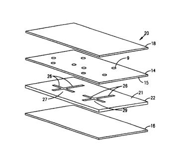
Referring now to Figs. lA, 1B, there is shown at 10 a portion of an embodiment
of an
S elongate flexible film laminate or microstructure device according to the
invention, as
assembled (Fig. 1 A) and in an exploded view in which the laminae appear as
separated (Fig.
1B). In Figs. lA and 1B, as in Figs. 2A, 2B, only a short segment of the full
length of the
laminate is shown, as suggested by broken lines indicating that the laminate
extends lengthwise
beyond the margins of the drawing. In the embodiment of Figs. lA, 1B, the
microchannel
structure is formed in a spacing lamina I 1 sandwiched between a base lamina
12 and a cover
lamina 14. Slits 16 having capillary cross-sectional dimensions are formed
through spacing
lamina 11, and are enclosed by apposed surfaces 13, I 5 of base lamina 12 and
cover lamina 14
in the composite structure. Fig. IB shows slits forming walls of just two 17,
19 of many
microchannel structures serially arranged lengthwise on the elongate laminate.
In the example
shown in Figs. lA, 1B, each microchannel structure has a simple cross
configuration formed
by enclosure of a pair of intersecting slits.
As will be appreciated, the widths of the microchannels resulting from the
construction
illustrated in Figs. lA, 1B is established by the width of the slits in the
spacing lamina; and the
thickness of the microchannels is established by the distance between the
apposed surfaces 13,
15 of the enclosing laminae 12 and 14, which approximates the thickness of the
spacing layer.
As noted above, the microchannels are of capillary dimension, that is, the
larger cross-sectional
dimension (usually the width) of the microchannel is usually no greater than
about 750 um,
more usually no greater than about 500 pm, and most usually in the range from
about 100 pm
to about 250 pm; and the smaller cross-sectional dimension (usually the depth)
can be
somewhat smaller.
Usually, as noted generally above, reservoirs or access ports or receptacles
are provided
for introducing the various components of the analytic process (sample,
bui~ers or solvents,
test compounds, etc. ) into the microchannel structures. These can be in the
form, for example,
of perforations 9 through the base lamina I2 or through the cover lamina 14,
as illustrated in
Fig. 1B. Where, as shown for example in Fig. 1B, the reservoirs or access
ports or receptacles
are formed in a lamina other than the one in which the channels are formed,
they must be
located so as to be suitably aligned with appropriate sites in the
microchannel structure when
CA 02306126 2000-04-13
WO 99/19717 PGTNS98/21869
-17
the composite is assembled. Accordingly, in Fig. I~, the perforations 9 in the
cover lamina 12
are arranged to be aligned with the ends of the microchannels formed in the
spacing layer 1 I
when the spacing lamina 11 is sandwiched between the apposed surfaces 13, 15
of the base
lamina 12 and the cover lamina 14.
To provide for predictable and consistent microfluidic movement, mixing, and
separations, the microchannels in the laminate composite device must be
adequately
dimensionally stable, and the apposing surfaces 13, 15 of the enclosing
laminae 12, 14 must be
adequately sealed to the surfaces of spacing lamina 1 I, at least at the
margins of the slits, to
keep the fluids within the flow paths formed by the microchannels from
escaping between the
laminae. These requirements are met by appropriate selection of materials and
thicknesses of
the~films making up the laminae, and by appropriate selection of means for
sealing the contact
surfaces of the laminae.
As noted above, each ofthe laminae is a flexible film, usually firm enough to
hold the
shape and dimensions of the microchannels, yet sufficiently compliant to
provide a desired
flexibility in the composite laminate device. Preferred films include acrylics
and polyethylenes,
for example. Preferred means for sealing will be selected according to the
film materials in the
laminae to be joined. Particularly, for example, the film materials and
adhesives described in
USSN 08/878,437 filed June 18, 1997 (Attorney Docket No. A-63519/RFTBK SOAN-
011),
the disclosure of which is hereby incorporated herein in its entirety.
In the embodiment ofFigs. IA, IB, the thickness ofthe spacing lamina is
selected to
provide the desired microchannel depth, taking into account any effect
(additive or subtractive)
that the sealing process may have on the distance between the apposed surfaces
13, 15 of the
enclosing laminae.
In addition to the spacing lamina 1 I and the enclosing laminae 12, 14, the
laminate may
further include release liners 16 and/or 18. Use of a release liner may be
especially desirable
where at least some of the components of the analytical process (a reagent or
a buffer, for
example) are provided on board the device prior to use. Such release liners
can mitigate
degradation or loss of the contents of the device during prolonged exposure to
varying
environmental conditions that may be encountered prior to use of the device,
as for example
during storage. It may be particularly important, for example, to avoid loss
or intrusion of
moisture or of more volatile substances out from or into the microchannel
structure. Or, it may
be important to avoid exposure to Eight. Accordingly, preferred release liners
form a barrier to
CA 02306126 2000-04-13
WO 99/I9717 PC'T/US98/21869
-18
movement of moisture or volatile materials, and thin polymer films, including
metallized filrrts
may be particularly suitable.
Referring now to Figs. 2A, 2B, there is shown at 20 a portion of an alternate
embodiment of an elongate flexible film laminate or microstructure device
according to the
invention, a assembled (Fig. 2A) and in an exploded view in which the laminae
appear as
separated (Fig. 2B). In this embodiment, the microchannel structures 27,29 are
constructed by
forming channels or trenches 26 in a surface 21 of base lamina 22, and
apposing a surface 15
of a cover lamina 14 onto surface 21 to enclose the microchannels. Reservoirs
or access ports
or receptacles can be provided for introduction of process components into
and/or for removal
of excess or waste from the microchannel structure, as noted with reference to
Figs. 1 A, 1B.
These are illustrated by way of example in Fig. 2A as perforations 9 through
cover lamina 14,
positioned so as to be suitably aligned with the channels or trenches 26 in
the base lamina. 22
when the surfaces 21, 15 of base lamina 22 and cover lamina 14 are apposed.
Alternatively, reservoirs may be provided in base lamina 22, in the form of
wells or
holes through the thickness of base lamina 22, each situated in fluid
communication with a
microchannel or trench, as may be desired. And, referring again to Figs. lA,
1B, reservoirs
may be provided in the spacing lamina 11, each in fluid communication with a
slit. If the base
lamina 22 (or the spacing lamina 11 ) is sufl'cciently thick, reservoirs of
significantly high
volume can be provided in this way, and the cover lamina (or enclosing
laminae) can be very
thin. For reservoirs that are loaded in the course of the lamination process,
no access opening
through either the cover lamina or the opposite surface of the base lamina (or
either of the
spacing laminae) is required; however, for any such reservoirs that are to be
loaded after the
laminate has been formed, access openings aligned with the reservoirs can be
provided, for
example as holes through the cover lanuna or through the base lamina (or
through a spacing
lamina).
In this embodiment the widths and depths of the microchannels are established
by the
dimensions of the trenches or channels formed in the base lamina. Accordingly,
precise control
of the dimensions during the formation of the trenches or channels, taking
account of any
additive or subtractive effect of the sealing process, results in reproducible
microchannel
dimensions.
As in the embodiment of Figs. 1 A, 1 B, the embodiment of Figs. 2A, 2B may
additionally include release liners 16 and/or 18.
CA 02306126 2000-04-13
WO 99/19717 -19- PCT/US98/21869
As in the embodiment of Figs. 1 A, 1 B, each of the laminae in the embodiment
of Figs.
2A, 2B is a flexible film. Preferred film materials for the base lamina 22 and
cover lamina 14
are polymer films; and preferred sealing means are selected according to the
film materials to
be joined. The base lamina 12 preferably is sufficiently thick to maintain its
structural integrity
after the trenches or channels have been formed in it. Particularly, for
example, where the
configuration of the microchannel structure is complex, or where there is a
high density of
trenches or channels, the mechanical strength of the base lamina may be
compromised, and for
ease of handling as well as to maintain the dimensionality of the microchannel
structure during
assembly and use, the base lamina should be thick enough so that it maintains
its mechanical
integrity.
Detection is usually optical, and most usually the signal is generated by
laser-induced
fluorescence; the detector is usually a conventional confocal optical system.
Other detections
means may be employed.
As noted above, each of the microchannel structures shown in Figs. 1B, 2B is
configured as a simple injection cross, formed by intersection of two straight
microchannels.
Such a configuration is useful, for example, in carrying out a quantitative
electrophoretic
separation of a metered sample volume, as described for example in U. S.
Patent Application
Ser. No. 08/878,447 filed June 18, 1997 [SOAN-017]. The intersecting
microchannels of a
simple injection cross need not be straight, and in some configurations more
efficient use of the
substrate area is made possible by configuring one or more microchannel arms
otherwise.
Referring now for example to Figs. 3A, 3B, alternative embodiments of simple
injection cross
configurations are shown in which one electrophoretic microchannel is made
relatively longer.
In each of nucrochannel structure configurations or microstructures 30, 32, a
shorter
microchannel and a longer microchannel intersect at 31 to form an injection
cross. Sample - V
supply reservoir 36, sample drain reservoir 37, elution buffer reservoir 33,
and analyte waste
reservoir 34 are provided at the ends of the microchannel segments; and an
electrode (not
shov~rn in the Figs.) connected to a source of electrical energy is positioned
to contact the
liquid contained within each reservoir. Potential differences across the
electrodes are adjusted
first to draw the sample electrokinetically from sample supply reservoir 36
across intersection
31 toward sample drain reservoir 37; and then to draw a metered volume of
sample from
intersection 31 into separation channel 35. As the sample plug proceed
electrokinetically
through separation channel 35 toward analyte waste reservoir 34, the sample
becomes
CA 02306126 2000-04-13
WO 99/19717 -20- PCT/US98I21869
electrophoretically separated into its analyte components, which are detected
at a downstream
detection region point in separation channel 35. As will be apparent in the
Figs., the
electrophoretic separation channel is made relatively much longer by forming
it as a spiral
turning one or more times around intersection 31 and reservoirs 33, 36, 37,
and the shorter
microchannel arms (Fig. 3A), or by foaming it in a folded confguration (Fig.
3B). The
resulting microchannel structures occupy a compact area of the substrate, and
can be
particulay useful in microchannel arrays, as will be described more fully
below with reference
to Fig. 4.
The microchannel structures can be formed in more complex configurations,
according
to the analytical process to be carreid out in them. Referring now to Fig. 3C,
there is shown by
way of example at 38 a microchannel structure or microstructure having an
intersection 31
forming an injection cross, and having sample supply reservoir 36, sample rain
reservoir 37,
elution buffer reservoir 33, and extended electrophoretic separation channel
35 leading to
waste reservoir 34. In this embodiment, microchannels enclosing flow paths
running from four
additional supply reservoirs 39 to four additional downstream drains 40
additionally cross the
microchannel downstream from the intersection 31. These additional flow paths
provide for
sequential introduction of four additional analytical components (which may be
reagents, or
test compounds, or buffers, etc.) to the moving sample plug.
An example of a microchannel array is shown in a plan view in Fig. 4,
illustrating a way
in which the arrangement of the microchannels structures in the array can be
made to match
the geometry of, for example, a standard 96-well plate. Such an arrangement
can facilitate
automated transfer of samples or of test compounds from the standard plate to
the continuous
form microchannel device of the invention, providing for efficient transfer
with reduced waste
and minimal cross-contamination. Fig. 4, for example, shows a short segment of
an elongate' -
flexible film laminate containing a series of microchannel arrays according to
the invention.
The elongate flexible film laminate 42 extends lengthwise beyond the range of
the drawing, as
indicated by broken lines extending from the edges 41 of the short segment.
The short segment
shown, which is limited by lines 43, includes two successive microchannel
arrays or
microstructures 44, 45. Each of the microchannel arrays 44, 45 in this example
contains 96
microchannel structures 30, each configured as in the example shown in Fig.
3A, and all
arranged in an orthogonal 12 X 8 grid that conforms to the geometry of a
conventional 96-well
plate.
CA 02306126 2000-04-13
WO 99/19717 PCTNS98/21869
-21
The basic technique and machinery for bringing the laminae together to form
the
laminate composite according to the invention are generally known, and,
depending upon the
materials that make up the various laminae, any of a variety of film
lamination techniques can
be used.
Figs. 5 and 6 are sketches showing in general outline schemes for constructing
the
laminate embodiments ofFigs. lA and 2A. Referring now to Fig. 5, there are
shown rollers 51,
52, and 54, carrying film materials to serve as, respectively, a spacing
lamina 11, a base lamina
12, and a cover lamina 14. Slits 16 may be cut through spacing lamina 11
before it is rolled
onto roller 51, so that the spacing lamina comes off roller 51 with the
configuration of the
mici~ochannel structures already in place; or, as illustrated in Fig. 5, a
cutting tool 57 may
operate to cut the slits in the predetermined pattern as spacing lamina 11 is
drawn from roller
51. Similarly, access openings or reservoirs 9 can be formed by perforating
base lamina 12 or
(as in Fig. 5) cover lamina 14 before it is stored on roller 54, so that
during assembly the cover
lamina comes off roller 54 with the perforations already in place; or, as
illustrated in Fig. 5, a
cutting tool 59 may operate to cut the predetermined pattern of perforations
as cover lamina
14 is drawn from roller 54. In either method, preferred tools for cutting
slits and perforations
include lasers (laser cutting or laser ablation) and die cutting, for example.
Laminae I 1, 12, and 14 are apposed by drawing them between rollers 53. As
will be
appreciated, it is essential that the perforated enclosing lamina be
appropriately aligned with
the spacing lamina during the lamination process, so that the perforations
will be suitably
aligned with the microchannels in the assembled device. Any registration
technique may be
used to ensure proper alignment in the longitudinal direction. Preferably,
sprocket holes can be
cut in one or both margins of the laminae, and the respective sprocket holes
can be aligned on
a sprocket. It can be suitable to provide a sprocket drive at the rollers 53,
for example.
As noted generally above, certain of the components of the analytic process to
be
carried out in the device (buffer or solvent, separation media, etc. ) can be
loaded into portions
of the microchannel structure before use. Particularly, it may be desirable to
load certain of the
constituents before enclosing the microchannels. This may be true, for
example, if one or more
constituents has a high viscosity at ambient temperatures, as may be true of
certain
electrophoretic separation media. Accordingly, as illustrated in Fig. 5, the
assembled laminate
formed of the spacing layer 11 enclosed by base layer 12 and cover layer 14 is
drawn through
CA 02306126 2000-04-13
WO 99/I9717 PGTNS98/21869
-22
a filling workstation 69, by conventional tractor means, where the selected
components are
injected or drawn by suction into the appropriate microchannels by way of the
access
perforations.
And, as noted above, where one or more components are provided on board the
device,
it maybe desirable to seat one or both surfaces of the device with release
Liners. Accordingly it
is optional, as shown in Fig. 5, as the assembled and filled laminate is drawn
toward takeup
roller 55, to draw release liners 16 and 18 from rollers 66, 68 and between
rollers 56, to
appose the release liners onto the surfaces of the enclosing Laminae 12 and
14. Alternatively,
where the nonperforated enclosing layer is impermeable to the contents of the
assembled and
filled microchannel laminate of spacing layer 11 and enclosing layers 12, 14,
sufficient
protection of the contents can be provided by the contact of the nonperforated
surface and the
perforated surface when the device is rolled onto takeup roller 55, on which
the device can be
stored for use.
Similarly, referring now to Fig. 6, there are shown rollers 64, 62, carrying
film materials
I S to serve as, respectively, a cover lamina 14 and a base lamina 22.
Channels or trenches 26 may
be formed in surface 21 of base lamina 22 before it is rolled onto roller 62,
so that the base
lamina comes off roller 62 with the configuration of the microchannels already
in place; or, as
illustrated in Fig. 6, a cutting tool (or other means, as described in more
detail below with
reference to Figs. 7 through 9) 67 may operate to form the trenches or
channels in the
predetermined pattern as base lamina 22 is drawn from roller 62. Suitable
cutting techniques
employ, for example, controlled laser ablation, using equipment and techniques
weal known in
the laser micromachining industry. Suitable laser micromachining systems and
protocols for
their use are available from, for example, Resonetics, Nashua, NH.
Other means for forming channels, cavities or trenches include but are not
limited for
heat embossing, hot embossing, ultraviolet embossing, ultraviolet curing of a
liquid substance,
patterning a thin film which extruding or hot stamping a surface of a film
layer prior to
lamination. Known micromachining techniques including. e.g., photolithographic
techniques,
may also be employed in forming the microstructures in the film surfaces.
Alternative methods
also include ultrasonic forming, pressure forming and thermal forming, vacuum
forming, blow
molding, stretch molding, insert molding, injection molding, extrusion
casting, compression
molding, encapsulation processes, thermoforming and digital printing, any of
which may be
CA 02306126 2000-04-13
WO 99/19717 PGTNS98I21869
-23
employed in a continuous-form process according to the invention. Any suitable
techniques
such as are known in the plastics micromachining art may be employed.
Similarly, access openings or reservoirs 9 can be formed by perforating cover
lamina 14
before it is stored on roller 64, so that during assembly the cover lamina
comes off roller 64
with the perforations already in place; or, as illustrated in Fig. 6, a
cutting toot 59 may operate
to cut the predetermined pattern of perforations as cover lamina 14 is drawn
from roller 64. In
either method, preferred tools for perforating the cover lamina include lasers
and die cutters,
for example, as described above with reference to Fig. 5, for example.
Laminae 14 and 22 are apposed by drawing them between rollers 63, and properly
aligned as described above with reference to Fig. 5.
here, as in the embodiment of Fig. 5, the assembled device can be provided
with one or
more of the analytical components on board. Components can be loaded into the
assembled
device by drawing the assembled laminate formed of the base layer 22 and the
cover layer I4
through a filling workstation 69, as described above with reference to Fig. 5.
And, optionally
where desired, as the assembled and filled laminate is drawn toward takeup
roller 65, release
liners 16 and 18 may be drawn from rollers 66, 68, and between rollers 56, to
appose the
release liners onto the surfaces of the laminate for protection.
In some embodiments according to the invention, the reservoir and microchannel
are
formed in the base lamina, and the flexible circuit laminate forms a cover
lamina. In one
approach, illustrated in Figs. 7a and 7b, the flexible circuit laminate (that
is, the cover lamina)
is made up of two layers, namely, a seal layer and a back layer. In this
embodiment part of the
conductive trace is formed on the back surface of the seat layer, and part is
formed in the front
surface of the back layer. In another approach, illustrated in Figs. 8a and
8b, the flexible circuit
layer is made up of three layers, namely a seal layer, which carries no
conductive trace, and'
two circuit layers, each carrying a conductive trace. One of these circuit
layers is a back layer,
and the other is laminated between the back layer and the seal layer.
Referring now to Figs. 7a, 7b, there is shown generally at 70 a portion of a
microstrocture device according to the invention, in transverse section thru a
reservoir and
microchannel and associated circuitry. The device consists of a base lamina
72, constructed of
a generally planar plastic material 74, a seal layer 76, formed of a low
fluorescence polymer
film 77, and a back layer 78, formed of a plastic film 79. Formed in the
polymer base lamina 74
are reservoir or well 71 and microchannel 73 of a microstructure. An opening
75 is formed
CA 02306126 2000-04-13
WO 99/19717 -24- PCTNS98/21869
through the seal layer film 77 in register with the reservoir 71. A front
surface of seal layer film
77 is provided with an adhesive 82, which will serve to seal the seal layer
and the base layer
together when assembled, as shown in Fig. 7b. A rear surface of the seal layer
is provided with
contact conductive trace portion or trace 83 of the circuitry. A detection
clearance opening 80
is formed through back layer film 79 in register with a detection zone of the
microchannel 73,
and a contact opening 8I is formed through back layer film 79 in register with
the contact
conductive trace portion 83. A front surface of the back layer film 79 is
provided with a
second conductive trace 85, having one region in register with a region of the
contact
conductive trace 83 and another region in contact with a carbon electrode or
electrode portion
86, which in turn is in register with the reservoir 71. A conductive adhesive
84 provides for
good conductive adhesion between conductive traces 83, 85, when assembled, as
shown in
Fig. 7b. It should be appreciated that layers 72, 76 and 78 can optionally be
sandwiched
between top and bottom release layers (not shown) similar to layers or liners
16,18 discussed
above. The top release layer can seal reservoir 71. The bottom release layer
can be provided
with openings in registration with openings 80,81 in the back layer 78.
Referring now to
Fig. 7b, an electrical contact or electrode probe 88 in the analytical
instrument contacts the
conductive trace portion or contact portion of the circuitry by way of the
contact opening in
the back layer, and a photodetector (not shown in the Figs.) detects the
signal in the
microchannel through the low fluorescence film of the seal layer by way of the
detection
opening 80 in the hack layer. Conductive traces 83,85 and carbon electrode 86
are included in
the electrical means of microstructure device 70.
Where laser-induced fluorescence detection is employed, preferred low
fluorescence
materials have sufficiently low fluorescence at the illuminating and back
scattering wavelengths
that the presence of the film in the optical path does not significantly
reduce detection. - -
Examples of suitable such materials include impact modified acrylic (e.g.,
Rohm film 99530),
polyethylene terephthalate ("PET"), polyolefins (e.g., Zeonex), and acetates.
The adhesive also
preferably has low fluorescence characteristics, and preferably has surface
characteristics
similar to those ofthe walls of the channel, inasmuch as the adhesive will
form one inner
surface of the microchannel when assembled, and differences could a
adversely affect electroflow in the channel. Suitable such adhesives include
organic based
acrylic adhesives.
CA 02306126 2000-04-13
WO 99/19717 PCT/US98lZ1869
-25-
Referring now to Figs. 8a, 8b, there is shown generally at 170 a portion of an
alternative embodiment of a microstructure device according to the invention,
in transverse
section thru a reservoir and microchannel and associated circuitry. The device
consists of a
base lamina 172, constructed of a generally planar plastic material 174, a
seal layer 176,
formed of a low fluorescence polymer film 177, a back circuit layer 178,
formed of a plastic
film 179, and an intermediate circuit layer 190, formed of a polymer film 191.
Formed in the
polymer base lamina 174 are reservoir or well 171 and microchannel 173 of a
microstructure.
An opening 175 is formed through the seal layer film 177 in register with the
reservoir 171. A
front surface of seal layer film 177 is provided with an adhesive 182, which
will serve to seal
IO the seal layer and the base layer together when assembled, as shown in Fig.
8b. A back surface
of the intermediate circuit layer film 191 is provided with contact conductive
trace portion or
trace 183 of the circuitry, and a front surface of the intermediate circuit
layer film 191 is
provided with an adhesive 192, which will serve to seal the intermediate
circuit layer film 191
to the seal layer 177 when assembled, as shown in Fig. 8b. An opening 195 is
formed through
the intermediate circuit layer 190, in register with the opening 175 in the
seal layer and with
the reservoir 171. An intermediate detection clearance opening 193 is formed
through
intermediate circuit layer film 191 in register with a detection zone of the
microchannel 173. A
detection clearance opening 180 is formed through back layer film 179 in
register with a
detection zone of the microchannel 173, and a contact opening 181 is formed
through back
layer film 179 in register with the contact conductive trace portion 183. A
front surface of the
back layer film 179 is provided with a second conductive trace 185, having one
region in
register with a region of the contact conductive trace 183 and another region
in contact with a
carbon electrode or electrode portion 186, which in turn is in register with
the reservoir 171. A
conductive adhesive 189 provides for good conductive adhesion between
conductive traces
183, 185, when assembled, as shown in Fig. 8b. It should be appreciated that
layers 172, 176,
178 and I90 can optionally be sandwiched between top and bottom release layers
(not shown)
similar to layers or liners 16,18 discussed above. The top release layer can
seal reservoir 171.
The bottom release layer can be provided with openings in registration with
openings 180,181
in the back layer 178. Referring now to Fig. 8b, an electrical contact or
electrode probe 188 in
the analytical instrument contacts the contact conductive trace portion or
contact portion of
the circuitry by way of the contact opening in the back layer, and a
photodetector (not shown
in the Figs.) detects the signal in the microchannel through the low
fluorescence film of the
CA 02306126 2000-04-13
WO 99/19717 PCT/US98/21869
-26
seal layer by way of the detection opening 180 in the back layer. Conductive
traces 183,185
and carbon electrode 186 are included in the electrical means of
microstructure device 170. In
this embodiment, the flexible circuit laminate (made up of the two circuit
layers) can be
constructed separately from the base layer and seal layer, because the seal
layer does not
include any cirwitry. Moreover, because in this embodiment there need not be a
good seal
between the flexible circuit laminate and the microchannels in the base layer,
it is not necessary
that the flexible circuit laminate have a surface that conforms precisely with
the surface of the
base layer.
An embodiment of a microstructure array device according to the invention,
provided
with flexible circuitry constructed generally as described above, is shown in
Figs. l la, l lb,
l lc. In this example, the elongate flexible film laminate contains a
plurality of microstructure
arrays arranged serially lengthwise along the laminate. Each microstructure
array in this
illustrative embodiment includes four microstructures, each configured to
carry out an analytic
process.
Referring now to Fig. 1 la, there is shown a short segment of an elongate
flexible film
base lamina or microstructure device 302 which extends lengthwise beyond the
range of the
drawing, as indicated by broken lines extending from the edges 310, 311 of the
short segment.
The short segment shown, which is limited by lines 303, includes two
successive microchannel
arrays 320, 321. Each of the microchannel arrays 320, 321 in this illustration
contains four
microstructures, two of which are indicated for example at 330, each
configured and designed
for carrying out a receptor binding assay, as described in detail in Example 1
below, with
reference to Fig. 9. Near the edge 310 and associated with each array is a pin
registration slot
326, and near the edge 3 I 1 and associated with each array is a pin
registration hole 327
Fig. I lb shows a corresponding flexible circuit laminate or microstructure
device 304,
which also extends beyond the range of the drawing, as indicated by broken
lines extending
from the edges 312, 313. The short segment shown, which is limited by lines
305, includes two
circuit layouts 322, 323, each configured to serve a microchannel array 320,
321 (shown in
Fig. l la) in the assembled device. The flexible circuit laminate can be
constructed generally as
described above with reference to Figs. 8a, 8b, for example. The circuits
consist of conductive
traces (two are shown at 332, for example) each connecting a contact terminal
(two are shown
at 333, for example) to four electrodes (334, for example) each located at a
point
corresponding to the positions of a reservoir in one of the four
microstructures in the array.
CA 02306126 2000-04-13
WO 99/19717 PCT/US98/21869
-27
Near the edges 312, 313, the flexible circuit laminate 304 is provided with-
pin
registration slots 328 and holes 329, associated with the circuit layouts such
that when the
base lamina and the flexible circuit laminate are assembled and the respective
slots and holes
are aligned, precise superposition of the electrodes over the respective
reservoirs is ensured.-
Referring now to Fig. 11 c, there is shown generally at 306 a short segment of
an embodiment
of an assembled continuous form microstructure device of the invention, made
by laminating
the base lamina ofFig. l la and the flexible circuit laminate ofFig. l lb. As
in Figs. l la, 1 lb,
the device extends beyond the range of the drawing, as indicted by broken
lines extending from
edges 314, 3 i5; and the short segment shown, which is limited by lines 307,
includes two
microstructure arrays 324, 325, each capable of carrying out four receptor
binding assays
under the control of the associated circuit layout.
The laminate is constructed, as described above, so that the contact terminals
are
accessible by contact points through contact holes in the cover film.
Accordingly, as the
laminate is carried through the analytical device, sets of contact points are
brought into contact
with the corresponding sets of contact terminate on the laminate device. The
contact points, in
turn, are connected to a source of electrical power, which is provided with
controls to change
the voltages at the electrodes in a pattern determined according to the
sequence of electroflow
manipulations to be carried out in the microstnuctures over the course of the
assay.
EXAMPLES
$, amine 1. Receptor Binding Assay
This Example illustrates a microstructure configuration and method for
carrying out a
membrane-receptor competitive binding assay according to the invention.
In this Example, cell membrane receptors are attached to solid-phase capture
media-for
facilitating the use of protein receptors in a microfluidic-based assay. Solid-
phase attachment
of the receptor can be achieved in one of several ways, including, e.g., the
use of activated
paramagnetic beads or other synthetic particles.
This assay is particularly applicable for receptors belonging to the seven
transmembrane
family or similar proteins wherein the sequence of amino acids traverses the
membrane
multiple times. These targets, eg., the G-protein coupled receptor (or GPCR),
are more likely
than others to require the physical environment of the membrane lipid bilayer
for
CA 02306126 2000-04-13
WO 99119717 -28- PCTIUS98121869
physiologically relevant interactions. The dopamine receptor is a specific
example. of the
broader class of GPCR proteins.
A membrane-receptor competitive-binding assay in regard to the above is
provided. The
non-isotopic assay comprises of two binding events. The primary receptor-
ligand affinity
reaction can be written generally as:
I-s + L~ + ~) - ~)-L~ + ~)-Li
"free" in "bound" in
supernatant solid-capture phase
where the library test compound Li and labeled ligand L~ compete for receptor
binding sites
(R) on the immobilized cell membrane protein. Once the unbound ligand L~,
which remains
"free" in the supernatant, is removed, then the bound ligand, which is
complexed with the
immobilized receptor beads, can be detected using a fluorophore-labeled
secondary binding
protein. If a biotinylated ligand is employed in the primary bioafflnity
reaction, then solid-
I S phase fluorescence detection is possible based on the following binding
reaction:
tR)-L~ + w* , (R)-L'~:*
where ~~* represents, for example, an avidin-fluorescein conjugate, as the
other member of the
secondary specific binding pair. Other protocols based on methods of the
invention are also
possible. For exampte, a detection scheme may be employed based upon depletion
monitoring
of the labeled ligand L'.
Such an assay can be carried out using a microfluidic assay device according
to the
invention, configured, in one embodiment, as shown generally at 100 in Fig. 9.
Referring now
to Fig. 9, there is shown an assay laminate or microstructure device 100, on
which the
microstructure is formed. The microstructure includes chambers and reservoirs
that are
connected in fluid communication by microchannels. Particularly, device or
card 100 includes a
zone 125 in which incubation is carried out and separation and detection can
be carried out; a
secondary capture and detection zone 135; a number of inlet reservoirs:
reservoir 102, which
serves as a supply of buffer solution; a reservoir 104, serving as a source of
library test
compound ligand i; reservoir 106, serving as a source of a biotin-labeled
ligand conjugate, or
biotinyated tracer; reservoir 108, serving as a source of fluorophore-labeled
secondary binding
protein, or fluorescent tracer, reservoir 110, serving as a source of bead-
immobilized,
membrane-bound receptor; wash buffer reservoir 112; reservoir 114, serving as
a source of an
agent that cleaves the fluorophore tag from the fluorescent tracer conjugate;
and capture
CA 02306126 2000-04-13
WO 99/19717 -29- PCT/US98I21869
compound source reservoir 116; and a number of outlet reservoirs: reservoir
124, to receive
waste from the binding assay from the fluorescent tracer conjugate; reservoir
I26, to receive
waste capture compound; and reservoir 128, to receive waste supernatant from
binding.
Each reservoir can be provided with an electrode that is connected to a source
of
electrical power, and potential differences among the various electrodes can
be controlled and
manipulated to selectively induce electrokinetic transport to and from the
reservoirs and within
the microchannels and chambers.
In preparation for the assay, the receptors are immobilized as follows.
Magnetic latex
beads, preactivated to covalently bind protein, are bound to a lectin such as
wheat germ
agglutinin (WGA). Upon completion of this step, unreacted or exposed bead
surface is
blocked from nonspecific interactions by incubation with a saturating
concentration of carrier
protein such as bovine serum albumin or gelatin. Then the WGA coated beads are
co-
incubated with coil membranes having on them the receptor of interest. This
interaction may
conclude with an additional blocking step, to remove or inactivate potential
sites of nonspecific
binding.
With reference again to Fig. 9, the bioanalytical assay proceeds on the
microfluidic
device 100 as follows.
1. A fixed quantity of receptor-bound beads are introduced into reservoir 110.
Then the
beads are transferred, by means of an applied magnetic field or electrokinetic
flow, to chamber
125 by way of a microchannel in fluid communication with the reservoir and the
chamber. In
this particular assay protocol, the beads are held in chamber 125 for the
duration of the
procedure.
2. Next, the compound I , to be tested for binding ability is moved from
reservoir 104
by electrokinetic means through communicating microchannels into chamber 125;
and either '
concurrently therewith or thereafter, a standard compound L~ of known binding
properties, is
moved from reservoir 106 into chamber 125. This latter compound L~ contains a
member of a
directly or indirectly detectable signal-producing system, for example,
covalently attached
biotin.
3. After an appropriate series of electrokinetically driven wash steps using
wash buffer
moved from reservoir 112, a determination is made for the amount of unknown
compound L;
that binds by determining the degree to which it displaces the standard
compound L~. This is
measured by introducing the secondary fluoro-labeled binding protein into
reaction chamber
CA 02306126 2000-04-13
WO 99/19717 PCTIUS98/21869
-30
125 from reservoir 108 and allowing the complex of compound and receptor, (R)-
L~, to react
with the streptavidin which binds biotin with high affinity. The amount of
streptavidin captured
is monitored directly when a fluorescent label is associated with the
streptavidin.
4. In some embodiments of the assay in this Example, the amount of fluorescent
label
associated with the membranes is determined by direct measurement in the
capture zone. In
other forms of the assay, the fluorescent label may be attached via a
disulfide bond (denoted by
""). This bond is readily cleaved under reducing conditions. Accordingly,
dithiothreitol, or
beta mercaptoethanol stored in reservoir 114 may be used to release the
fluorescent label
(denoted by "*").
5. The fluorescent labeled species can then be separated from other reactants
by
electrokinetic or hydrodynamic enhanced electroseparation techniques. To
facilitate detection,
the magnetic beads may be immobilized at a site along the capillary path 125
by application of
a magnetic field. The fluorescent label may be detected at that site or at a
site 135 downstream
therefrom. The fluorescent label may be detected in the fluorescent labeled
species, or the
fluorescent label may be cleaved and detected separately.
)nple 2. Enzyme Assay.
This Example illustrates a microstructure configuration and method for
carrying out an
enzyme assay according to the invention, which can be particularly useful in
high-throughput
pharmaceutical drug discovery and screening applications.
In this Example, an enzyme, a labeled substrate, and an inhibitor are mixed
and allowed
to incubate, and then the labeled product of the enzymatic reaction and the
labeled unreacted
substrate are separated electrophoretically and each is quantitatively
determined by detection
of the label. - -
Such an assay can be carried out using a microfluidic assay device according
to the
invention, configured, in one embodiment, as shown generally at 200 in Fig.
10. Referring now
to Fig. 10, there is shown an assay laminate or microstructure device 200 on
which the
microstructure is formed. The microstructure includes an incubation chamber
250, an injection
cross 275, an electrophoretic separation channel 285, and detection zone 295,
connected in
fluid communication by microchannels with a number of reservoirs, including
inlet reservoirs:
reservoir 202, for supply of enzyme, which is usually a kinase, and containing
ATP and Mg2+;
reservoir 204, for supply of labeled substrate S *, which is usually a
fluorophore-labeled
CA 02306126 2000-04-13
WO 99/19717 PCTNS98/218b9
-31
peptide; reservoir 206, for supply of enzyme inhibitor; reservoir 218, serving
as a supply of
assay buffer, and employed to electrokinetically transport the product mixture
stream to an
outlet reservoir 228; and reservoir 236, serving as a supply of running
buffer, and employed to
electrokinetically transport a metered plug of the product mixture into the
separation channel
S 28S and the outlet reservoir 246; and a number of outlet reservoirs:
reservoir 214, to receive a
mixture of excess enzyme, substrate, and inhibitor; reservoir 228, for
receiving product
mixture stream; and reservoir 246, for receiving detection product waste.
Each reservoir can be provided with an electrode that is connected to a source
of
electrical power, and potential differences among the various electrodes can
be controlled and
manipulated to selectively induce electrokinetic transport to and from the
reservoirs and within
the microchannels and chambers.
In some particularly useful embodiments, the enzyme inhibitor is a
pharmaceutical drug
candidate, and the assay is carried out to determine the effectiveness of the
candidate as an
inhibitor for the particular enzyme. Usually the enzyme is a tyrosine specific
protein kinase
1S such as, for example, Src kinase; and usually the labeled substrate is a
fluorophore-labeled
peptide such as, for example, cdc-2 peptide.
The enzyme assay proceeds on the microfluidic device 200 as follows.
1. Mixing. Reagents are moved electrokinetically from inlet reservoirs 202
(enzyme),
204 (substrate), and 206 (inhibitor) toward outlet reservoir 214. Mixing of
the reagents
occurs in mixing cross 22S and in incubation chamber 250.
2. Incubation. The fluid flow is hatted electrokinetically by adjustment of
the various
potentials in order to let enzyme, substrate and inhibitor incubate in
incubation chamber 225.
3. Injection. A continuous stream of the product and excess reagent mixture
are moved
out from the incubation chamber 250 and into the outlet reservoir 228, using
the inlet reservoir
2S 218 as the source of the assay buffer to electrokinetically drive the fluid
transport.
4. Separation. A plug of the product mixture is electrokinetically injected
from the
injection cross 275 into the electrophoretic separation channel 28S and then
into waste outlet
reservoir 246 using inlet reservoir 236 as the source of the running buffer to
electrokineticaliy
drive the fluid transport. As a result of mobility shift produced by
conversion of labeled
substrate S* to product P*, S* and P* are separated electrophoretically as
they are
electrokinetically transported in separation channel 285. Laser-induced
fluorescence
monitoring of the labeled substrate and product is achieved in the detection
zone 295. Because
CA 02306126 2000-04-13
WO 99/19717 PCT/US98/21869
-32
the mobility shift is usually expected to result from differences in
charge/mass ratio between S*
and P*, a gel matrix is usually not required to achieve separation.
As the Examples illustrate, the invention is useful in a wide variety of
applications
involving techniques and protocols in fields of, for example, cell biology,
molecular biology,
HI.A tissue typing, and microbiology. More specifically, for example, the
invention can be
applied to techniques for immunodiagnostics, DNA purification from whole blood
and other
samples, mRNA isolation, solid phase cDNA synthesis, receptor-binding assays,
drug
screening and discovery, and cell isolation.
Other embodiments are within the following claims. For example, assay devices
other
than microchannel devices can be adapted in a continuous form assay array
format generally as
described herein, to provide high throughput systems. For example, the fluids
{reagents,
samples, etc.) employed in the assay can be mixed and measured in wells (that
is, in cavities)
constructed in an elongate laminate device, and not necessarily directed by
microfluidic
manipulation.
And, for example, microstructures or arrays of microstructures may be formed
in more
than one lamina in the laminated device according to the invention, so that
microstructures in
one lamina are superimposed over microstructures in another. The superimposed
microstructures may, for example, carry out different but related processes or
process steps in
a fluidic process and, by providing for fluid communication between the
laminae, fluids may be
transported from one mjcrostructure to another in the course of the process.
This permits
related processes to be carried out in close proximity under similar
conditions, and without a
need for transfer of products or byproducts or intermediates from one reaction
container (or
from one microstructure) to another. Fluid communication between laminae can
be provided
by, for example, simply perforating the layer that separates the
microstructures, and control of
the flow through such a perforation can be done, preferably in a valueless
fashion, by any of
the various means employed for moving fluids within the microstructure of a
lamina.
As will be appreciated, although the device according to the invention is
described
above as being used in continuous processing form, individual microstructures
or arrays in an
elongate laminate made as described above can be separated one from another,
and used as
discrete devices in "card" form, each containing a microstructure or an array
of
microstructures. As may be desired, the elongate laminate may, where such use
is
contemplated, be made easily separable between successive microstructures or
arrays, for
CA 02306126 2000-04-13
WO 99/19717 -33- PCT/US98/21869
example by perforating or scoring the laminate, or cutting the laminate
partway through. Use
of the laminate in this way preserves the advantages of continuous form in the
manufacture of
the device, and replaces advantages of using the device in continuous form
with advantages of
handling discrete card-form microfluidics devices.
Approaches to aligning the Laminae during manufacture other than through holes
or
notches can be used, for example, techniques employing optical, electrical,
and ultrasonic
alignment, or employing other mechanical means such as ratchets.
It should be appreciated that any of the microstructure devices described
above,
including those manufactured in accordance with the processes shown in Figs. 5
and 6 and
described above, can be cut or diced into a plurality of discrete card-like
microstructure
devices, each having a plurality and more specifically an array of discrete
microstructures
formed therein. Such card-like devices can be used for any of the uses
described above.
Although such card-like devices can be of any suitable size, in one preferred
embodiment such
devices can be sized on the order of a credit card.
Another embodiment of the microstructure device of the present invention is
shown in
Figs. 12 and 13. Microstructure device 406 therein is formed from a laminated
structure
having a plurality of separate layers or laminae joined together.
Microstructure device 406 is
preferably a discrete or card-like device, but can also be an elongate
flexible device suitable for
storage on a reel. The microstructure device 406 is for use with a contact
probe assembly 409
having a plurality of contact probes 411 arranged in a predetermined pattern
on any suitable
support structure 412, shown in Fig. 12 as being a body 412 having a planar
surface 413. The
elongate contact or electrode probes 411 are made from any suitable conductive
metal and in
the embodiment of the contact probe assembly 409 shown in Fig. 12 are needle-
like in
conformation and preferably compliant vertically to facilitate electrical
coupling with ' -
microstructure device 406. Each of the probes 411 is formed with a rounded end
411 a. The
probes 411 extend perpendicularly from surface 413 in a predetermined pattern.
Although
probes 411 are shown as rigidly mounted on support structure 412 so as to
remain static
during operation, the probes can be mounted on the support structure 412 for
retraction and
extension from a plurality of bores that open onto surface 414. Separate
electrical leads (not
shown) are carried by support structure 412 for connection to each of the
contact probes 411.
Such leads are, in turn, connected serially or separately to a controller (not
shown) which
CA 02306126 2000-04-13
WO 99/19717 -34- PCTNS98I21869
provides appropriate electrical signals, preferably in the form of voltage
potentials, to the
probes 411.
Microstructure device 406 has a thickness ranging from approximately 100
microns to
three millimeters and preferably ranging from approximately 150 microns to one
millimeter.
The microstructure device 406 includes a laminate structure 421 having first
and second
spaced-apart planar surfaces 422 and 423 which form two exterior surfaces of
the laminate
structure 42i (see Fig. 13). A first layer or lamina 426 is included within
laminate structure
421. The first lamina or card body 426 is made from any suitable nonconductive
material such
as plastic and can be relatively rigid or flexible depending on the particular
use of
microstructure device 406. In one embodiment of a card-like device 406, the
first lamina 426
is relatively rigid to provide rigidity to the device 406. Alternatively,
other layers in the
laminate structure 421 can be relatively rigid, in addition to or instead of a
rigid lamina 426, if
a rigid microstructure device 406 is desired. First lamina 426 has a first
planar surface in the
form of ftrst or top surface 422 and a second planar surface 427 spaced apart
from the top
surface 422 and interior of the laminate structure 421.
The laminate structure is provided with at least one microstructure 428 of
capillary
dimensions, and preferably a plurality of microstructures 428, formed therein
and extending in
a direction parallel to the parallel surfaces 422 and 427 of the first lamina
426. For simplicity,
only one microstructure 428 is shown in Fig. 12. More specifically, each of
the
microstructures 428 is formed in first lamina 426 and extends through one of
the planar
surfaces 422, 427 of the first lamina. As shown in Fig. 13, microstructures
428 open onto
second or lower surface 427 of the first lamina 426. Each microstructure 428,
as shown in
Fig. 12, preferably includes at least first and second microchannels 431 and
432 which meet at
an intersection 433. Laminate structure 421 is provided with at least one and
as shown a -
plurality of holes or wells 436 in fluid communication with each
microstructure 428. In one
preferred embodiment of microstructure device 406, first and second wells 436a
and 436b are
provided at the first and second end portions of first microchannel 431 and
third and fourth
wells 436c and 437d are provided at the first and second ends of second
microchannel 432. It
should be appreciated that the wells 436 can be provided at other locations
within
microstructure 428 and be within the scope of the present invention. Each of
the wells 436, as
shown with respect to first well 436a in Fig. 13, is adapted to receive a
fluid and consists of a
bore extending between surfaces 422, 427 of first lamina 426 and is accessible
from the top
CA 02306126 2000-04-13
WO 99/19717 -35- PCTIUS98/21869
surface 422 of the laminate structure 421. Wells 436 can be sized to receive
approximately
one microliter of such fluid.
Laminate structure 421 includes a second layer or lamina 441 made from any
suitable
non-conductive material such as plastic. Second lamina or film 441 has a first
planar surface
442 and a second planar surface in the form of second or bottom surface 423
which is spaced-
apart from and parallel to the top surface 422. Second lamina 441 is secured
to first lamina
426 by any suitable means such as an adhesive layer 443 disposed between
surfaces 427 and
442. In an alternative embodiment, surfaces 427 and 442 can be diffusion
bonded together
and adhesive layer 443 thus eliminated.
A plurality of electrical means 444 are at least partially carried by second
lamina 441.
The electrical means 444 are preferably equal in number to the number of wells
436 provided
in laminate structure 421 such that each of the wells 436 has a corresponding
electrical means
444. Each of such electrical means 444 includes an electrode portion 444a in
communication
with any fluid provided in the welt 436 and a contact or pad portion 444b
spaced apart from
electrode portion 444a and not in contact with any such fluid in well 436. An
interconnect
portion 444c connects the electrode portion 444a to the contact portion 444b.
In the
embodiment of the microstructure device shown in Figs. 12 and I3, each
electrical means 444
extends through a bore 446 between surfaces 442 and 423 of the second lamina
441 such that
the electrical means resembles a circular plug or disk disposed in the second
lamina 441. Bore
446 has a diameter smaller than the diameter ofwell 436 so as to minimize
fluid contact with
the material of electrode portion 444a. The electrical means 444 are each made
from any
suitable material such as conductive carbon ink. Conductive metals such as
silver, copper,
gold, platinum and palladium, other conductive inks such as metalized inks and
blends of
conductive materials and polymers such as conductive epoxies and conductive
adhesives are
also suitable materials for electrical means 444. Electrode portion 444a is
disposed adjacent
first or upper surface 442 of the second lamina and interconnect portion 444c
is disposed in
bore 446. Contact portion 444b is disposed adjacent bottom surface 423 of the
second lamina
441 and underlying the electrode portion. The contact portion 444b can extend
downwardly
from bottom surface 423 and have a rounded end as shown in FIG. I 3. The
diameter of the
contact portion 444b is larger than bore 446 so that a portion of the contact
portion sits on the
bottom surface 423 for facilitating retention of the electrical means 444 in
bare 446 during
engagement with contact probes 411. Electrode portion 444a and contact portion
444b are
CA 02306126 2000-04-13
WO 99/19717 PCTIUS98/21869
-36
aligned with the respective welt 436 and electrode portion 444a forms at least
a portion of the
bottom surface of such well 436.
Contact portions 444b are accessible from the exterior or bottom surface 423
of
laminate structure 421 and microstructure device 406 without need of
penetrating any of the
layers of such structure 421 and device 406. In addition, contact portions
444b are arranged
on bottom surface 423 in a pattern which corresponds to the predetermined
pattern of contact
probes 411. As such, the contact probes 411 can register with and
simultaneously or
otherwise engage respective contact portions 444b when microstructure device
406 and
support structure 412 are moved relative to each other into close proximity
with each other.
Microstructure device 406 can optionally include a third layer or lamina 448
made from
any suitable material such as plastic. The third lamina 448 overlies each of
wells 436 and is
secured to iaminate structure 421 by any suitable means such as heat bonding
so as to suitably
secure any fluid located within the wells. Alternatively, the cover lamina 448
can be
removably or temporarily secured to the laminate structure 421 by an adhesive
or any other
suitable means to permit removal and reattachment of the cover lamina. The
third lamina 448
has a first or upper planar surface 451 which serves as an exterior surface of
microstructure
device 406 and a second or lower planar surface 452 which is adhered to top
surface 422 of
laminate structure 421 by a pressure sensitive adhesive, heat bonding or any
other suitable
means.
In operation and use, a fluid and preferably a liquid is provided in each well
436. A
fluid 453 is shown in Fig. 13 in first well 436a. Such fluids can be supplied
to wells 436 during
manufacture of microstructure device 406 or immediately prior to use of the
device 406 and
can be a single fluid or a plurality of fluids of different composition.
Fluids can be sealed in the
wells 436 by means of third or cover lamina 448. Cover lamina 448 permits
fluids to be
supplied to wells 436 during manufacture of the device 406 and stored therein
during
transport. Prior to use, the cover lamina 448 can be pierced if additional
fluids need be added
to one or more wells 436 or, if the cover Lamina 448 is removable, removed for
the supply of
such additional fluids and optionally reattached thereafter. Cover lamina 448
advantageously
inhibits evaporation of fluids contained in wells 436 and microstructures 428.
Contact portions 444b and contact probes 411 are brought into engagement to
permit
electrical coupling thereof. In this regard, microstructure 406 can be placed
upon contact
probes 411 or, alternatively, contact probes 41 I brought into contact with
the microstructure
CA 02306126 2000-04-13
WO 99/19717 PCTIUS98/21869
_37_
device 406. In either instance, contact probes 411 simultaneously engage
respective contact
portions 444b. A force can optionally be applied to the top surface of
microstructure device
406 to enhance electrical contact between contact portions 444b and contact
probes 411. A
distributed force can be applied to the top surface of device 406 by means of
pressurizing the
top surface in a conventional manner with any suitable fluid such as air or
argon gas.
Microstructure devices 406 can be used in any of the processes described or
referenced
above. During such processes, the fluids provided in wells 436 can be
electroltinetically
transported through microstructure 428 by means of voltage differentials
provided between
appropriate wells 436. Probes 411 provide a predetermined voltage potential to
one or more
electrode portions 444a when such voltage potential is supplied by the
controller. The
sequence and timing of such voltage potentials determine the manner in which
fluids flow
through microstructures 428.
It should be appreciated that all or portions of cover lamina 448 and laminate
structure
421 can be made from materials which are optically transparent so as to permit
optical
detection of the fluids within microstructures 428 and/or wells 436.
Alternatively,
microstructure device 406 can be adapted for use with other conventional
detection devices
for determining characteristics of the fluids within microstructures 428
and/or wells 436.
Microstructure device 406 permits electrical potentials to be provided to each
of the
wells 436 therein without the net of contact probes 411 being inserted
directly into the fluid
within such wells. Instead, electrical probes 411 each engage a contact
portion 444b which
transmits the electrical potential of the contact probe 411 to electrode
portion 444a in contact
with the fluid within the well 436. Contact probes 411 are thus not
contaminated with the
fluid of the wells 436 and can be used in the operation of a second
microstructure 406 without
fear of mixing the fluids from the first microstructure device with the fluids
in the second V
microstructure device. As can be seen, contact probes 411 can be repeatedly
used in a process
which sequentially analyzes and/or detects characteristics of fluids supplied
to a plurality of
microstructure devices 406. The close proximity of the electrode portions 444a
to the contact
portions 444b inhibit current losses in the electrical means 444.
Microstructure device 406 can be used in the manner discussed above with other
contact probe assemblies. For example, a portion of another contact probe
assembly 456 is
shown in Fig. I3. The assembly 456 is substantially similar to probe assembly
409 except that
a plurality of traces pads 457 are arranged on body 413 in a predetermined
pattern instead of
CA 02306126 2000-04-13
WO 99/19717 PCT/US98/21869
-38-
contact probes 411. Each pad 457, one of which is shown in Fig. 13, is formed
~n an
electrical trace 458 disposed on surface 414 of the body. The traces 458 are
made from any
suitable material such as copper, sliver, platinum, palladium, conductive
carbon or platinum-
laden polymers and other conductive inks such as metalized inks and blends of
conductive
materials and polymers such as conductive expvxies and conductive adhesives
formed on
surface 414. These materials can be so disposed on surface 414 by vapor
deposition, screen or
other printing, other traditional flex circuit methods or any other suitable
means. Trace pads
457 can be made from any suitable material such as gold and/or the materials
listed above for
traces 458 and be formed on the end of the respective trace by any of the
methods discussed
above with respect to the traces 458. The bulbous contact portions 444b of
microstructure
device 406 depend from bottom surface 423 so as to facilitate electrical
contact between the
contact portions 444b and pads 457.
In another embodiment, a microstructure device 461 substantially similar to
the
microstructure device 406 and for use with contact probe assembly 409 is shown
in Fig. 14.
Like reference numerals have been used to describe like components of
microstructure devices
406 and 461. A laminate structure 462 substantially similar to laminate
structure 421 is
included within microstructure device 461. A second layer or lamina 463 is
included in
laminate structure 462 and has a first or upper planar surface 466 and a
second planar surface
in the form of bottom surface 423 of the laminate structure 462. Although the
second lamina
463 is shown as being secured to first lamina 426 by an adhesive layer 467, it
should be
appreciated that surfaces 427 and 466 can be heat bonded or sealed together by
any other
suitable means. Microstructure device 461 is shown with a cover lamina 448,
but it should be
appreciated that the device 461 can be provided without a cover lamina 448 so
that wells 436
are each accessible from the top surface or exterior of microstructure device
461. -
A plurality of electrical means 471 are at least partially carried by second
lamina 463.
The electrical means 471 are preferably equal in number to the number of wells
436 provided
in laminate structure 462 such that each of the wells 436 has a corresponding
electrical means
471. Each of such electrical means 471 includes an electrode portion 471 a
which can
communicate with the fluid supplied to the well 436 and a contact or pad
portion 471b spaced-
apart from electrode portion 471a and not in fluidic contact with any such
fluid. Electrical
means 471 each include a trace portion or trace 471 c which electrically
connects the respective
electrode 471a to the contact portions 471b. As can be seen from Fig. 14,
contact portion 471
CA 02306126 2000-04-13
WO 99/19717 PCT/US98121869
-39
is disposed adjacent and more specifically formed on bottom surface 423.
Electrical trace
471 c extends from the contact portion through a passage 472 extending
transversely and more
specifically diagonally between surfaces 466 and 423 of the second lamina 463
and has a
further portion disposed on the upper surface 466 underlying electrode portion
471a. Second
lamina 463 can be made from any suitable flex circuitry material such as
acrylic, polyimide or
PET. Contact portions 471 b and portions of trace 471 c can be formed from any
suitable
material such as copper, silver, platinum, palladium, conductive carbon or
platinum-laden
polymers and other conductive inks such as metalized inks and blends of
conductive materials
and polymers such as conductive expoxies and conductive adhesives formed on
the
aforementioned surfaces of second lamina 463. These materials can be so
disposed on such
surfaces of the second lamina by vapor deposition, screen or other printing,
other traditional
flex circuit methods or any other suitable means. Electrode portions 471 a can
be formed from
any suitable material such as gold and/or the materials listed above for
contact portions 471b
and traces 471 c and be formed on trace 471 c by any suitable means such as
those described
above with respect to contact portions 471b and traces 471c. Each of the
electrode portions
471a is shown as forming at least a portion of the bottom surface of the
respective well 436.
Alternatively, the electrode portions 471a can form the entire bottom surface
of the well 436
or merely make fluidic contact with the well from a side wall or otherwise.
Contact portions
471b are accessible from the exterior or bottom surface 423 of laminate
structure 461 and
microstructure device 461 and are each preferably spaced-apart from the
centerline of the
respective well 436. The contact portions 471b are arranged on the underside
of
microstructure device 461 in a pattern corresponding to the pattern of contact
probes 411 on
support structure 412.
Microstructure device 461 can be operated with contact probes 411 in
substantially the
same manner as described above with respect to microstructure device 406.
Rounded ends
411a of the contact probes 411 can simultaneously engage the contact portions
471b for
providing the desired electrical potential to the fluid in each of wells 436.
Microstructure device 461 can also be used in the manner discussed above with
other
contact probe assemblies. For example, a portion of another contact probe
assembly 476 is
shown in Fig. 14. The assembly 476 is substantially similar to probe assembly
409 except that
a plurality of traces pads 477 are arranged on body 413 in a predetermined
pattern instead of
contact probes 411. Each pad 477, one of which is shown in Fig. 14, is formed
on an
CA 02306126 2000-04-13
WO 99/19717 PCT/US98I21869
-40
electrical trace 478 disposed on surface 414 of the body. The traces 478 are
made from any
suitable material such as those described above with respect to traces 457 of
contact probe
assembly 456 and are disposed on surface 414 by any suitable method such as
those discussed
above with respect to traces 457. Trace pads 477 can be made from any suitable
material such
as those described above with respect to electrical means 444. The bulbous
trace pads 477
extend upwardly from surface 414 and traces 478 of contact probe assembly 476
so as to
facilitate electrical contact between the contact portions 471 b and trace
pads 477.
A further embodiment of a microstructure device of the present invention is
shown in
Figs. 15 and 16. Microstructure device 481 therein is substantially similar to
microstructure
devices 406 and 461 and is for use with contact probe assembly 409. Like
reference numerals
have been used to describe like components of devices 406, 461 and 481. A
laminate structure
482 substantially similar to laminate structure 421 is provided in
microstructure device 481.
Laminate structure 482 includes a first layer or lamina 483 which is
substantially similar to f rst
lamina 426 and has first and second planar surfaces 486 and 487 extending in
parallel
directions. At least one and preferably a plurality of microstructures 428 are
provided in
laminate structure 482. One of microstructures 428 is shown in Fig. i 5 and a
portion of such
microstructure 428 is shown in Fig. 16. The microstructures 428 are formed in
laminate
structure 482 in the same manner as they are formed in laminate structure 421.
Specifically,
each of the microstructures 428 is formed in first lamina 483 and opens onto
second or lower
surface 487 of the lamina 483. A plurality of wells 436 extend between
surfaces 486 and 487
in fluid communication with the microstructure 428 and are each accessible
from first or top
surface 486 of laminate structure 482.
Laminate structure 482 includes an optional second layer or lamina 488 made
from
plastic or any other suitable material. Thin film or lamina 488 has a first or
upper planar -
surface 491 and a second or lower planar surface 492 parallel to the upper
surface 491. The
upper surface 49I is secured to the lower surface 487 of first lamina by
diffusion bonding or
any other suitable method. A bore 493 having a diameter substantially equal to
the diameter of
the well-forming bore in first lamina 483 extends between surfaces 491 and 492
for forming a
part of well 4366. The combined thicknesses of laminae 483 and 488 determine
the depth of
wells 436. If a thin layer film is used for second lamina 488, the thickness
of first lamina 483
can be increased to provide the desired depth to wells 436.
CA 02306126 2000-04-13
WO 99/19717 PCT/US98/21869
-4 I
A third layer or lamina 496 is included in laminate structure 482. The third
lamina 496
is substantially similar to second lamina 463 and has a first or upper planar
surface 497 and a
second or lower planar surface 498. Upper surface 497 of the third lamina 496
is secured to
lower surface 492 of second lamina 488 by an adhesive layer 499 or any other
suitable means.
Upper surface 486 of the first lamina and lower surface 498 of the third
lamina 496 form the
top and bottom surfaces of laminate structure 482.
A plurality of electrical means 501 are at least partially carried by third
lamina 496 for
each microstructure 428 such that each of the wells 436 has a corresponding
electrical means
501. More specifically, each electrical means 501 is disposed on upper surface
497 of the third
lamina 496. Each such electrical means 501 has an electrode portion SOI,a, a
pad or contact
portion 501 b and a trace portion or trace 501 c. The electrical trace 501 c
is made from any
suitable material such as any of the materials discussed above with respect to
contact portions
471b and traces 471c and is disposed on upper surface 497 by any suitable
means such as any
of those described above with respect to contact portions 471 b and traces 471
c. The trace
501 c has a first end portion underlying the respective well 436 and a second
spaced-apart end
portion underlying an access bore 502 extending between upper and lower
surfaces 486 and
487 of the first lamina 483 and an access bore 503 extending between upper and
lower
surfaces 491 and 492 of second lamina 488. Electrode portion SOla consists of
a layer of
material disposed on the first end portion of trace 501 c underlying well 436.
Electrode portion
501 a is shown in Fig. 16 as forming at least a portion of the lower surface
of the well 436.
Contact portion SOIb consists of a layer of material disposed on the opposite
second end
portion of trace 501 c and serves as the lower surface of access bores 502 and
503. Adhesive
layer 499 extends around the base of bore 493 and over the portion of trace
501 c between
electrode portion SOl a and contact portion 501 c to provide a fluid seal at
the bottom of the
well 436. The electrode portion SOIa and the contract portion SOIb can each be
made from
. any suitable material such as any of the materials discussed above with
respect to electrode
portions 471a and can be formed by any suitable means such as any of those
described above
with respect to contact portions 471 b and traces 471 c. Contact portions 501
b are arranged on
the bottom surface 498 of laminate structure 482 in a pattern corresponding to
the pattern of
contact probes 411 on support structure 412 and are accessible from such
bottom surface 498.
Microstructure device 481 can optionally include a fourth layer or lamina 506
substantially similar to cover lamina 448 and having a first or upper surface
507 and a second
CA 02306126 2000-04-13
WO 99/19717 PCTIUS98/21869
-42
or cower surface 508 heat bonded or otherwise suitably secured to upper
surface-486 of the
first lamina 483. Cover lamina 506 overlies each of wells 436 so as to
sealably secure the fluid
453 within the well. An opening 509 is provided in cover lamina 406 in
registration with
access bores 502 and 503 for permitting contact probes 411 to engage contact
portions SOIb.
Microstructure device 481 can be operated in substantially the same manner as
described above except that contact probes are disposed above the device 481.
In this regard,
contact probes 41 I are positioned above microstructure device 481 such that
rounded ends
411a ofthe contact probes 411 face downwardly toward openings 509 and contact
portions
SOIb. When it is desired to transport fluids within microstructures 428, the
microstructure
device 481 and contact probes 411 are moved relative to each other such that
rounded ends
411a enter openings 509 and electrically engage contact portions SOIb.
The engagement of contact probes 411 with the top of microstructure device 481
allow
less obscured access to the bottom of device 481 for purpose of optical
detection and/or
temperature control. Second lamina 488 provides an opposing surface 491 to the
microstructures 428 formed in the first lamina which is not an adhesive. The
inclusion of the
second lamina 488 facilitates forming microstructures 428 from walls that are
all of the same
material, which can be advantageous in certain processes of device 481. In
addition, the
absence of fluid contact with the adhesive permits a broader selection of
adhesives to be
considered for adhesive layer 499.
An embodiment of another microstructure device is shown in Fig. 17 where a
portion of
nucrostructure device 521 is depicted. The microstructure device 521 is
substantially similar
to microstructure device 406 and like reference numerals have been used to
describe like
components of devices 406 and 521. A laminate structure 522 substantially
similar to laminate
structure 421 is provided. A first lamina 426 having a plurality of
microstructures 428 formed
therein is included in the laminate structure 522. For simplicity, a portion
of only a single
microstructure 428 and one of the plurality of wells 436, specifically first
well 436a, is shown
in Fig. 17. A second layer or lamina 523 made from any suitable flex circuit
material such as
acrylic, polyimide or PET is included within laminate structure 522 and has a
first or upper
planar surface 526 and a second or lower planar surface in the form of bottom
surface 423 of
the laminate structure 522. Although the second lamina 523 is shown as being
secured to first
lamina 426 by an adhesive layer 527, it should be appreciated that surfaces
427 and 528 can be
heat bonded or sealed together by any other suitable means. Microstructure
device 521 is
CA 02306126 2000-04-13
WO 99/19717 PCT/US98/21869
-43
shown with a cover lamina 448, but it should be appreciated that the device
521 can be
provided without a cover lamina so that wells 436 are each accessible from the
top surface or
exterior of microstructure device 521.
A plurality of electrical means 531 for each microstructure 428 are at least
partially
carried by second lamina 523 such that each of the wells 436 has a
corresponding electrical
means 531. More specifically, each electrical means 531 is disposed on upper
surface 526 of
the second lamina 523. Each such electrical means 531 has an electrode portion
531 a, a pad
of contact portion 53 lb and a trace portion or trace 531 c. Trace 531 c is
made from any
suitable material such as any of the materials discussed above with respect to
contact portions
471b and traces 471c and is disposed on upper surface 526 by any suitable
means such as any
of those described above with respect to contact portions 471 b and traces 471
c. The trace
531c has a first end portion underlying the respective well 436 and a spaced-
apart second end
portion underlying a recess or cavity 532 formed in first lamina 426 and
opening onto lower
surface 427 thereof. Electrode portion 53 la consists of a layer of material
deposited on the
first end portion of trace 531 c underlying well 436 and is shown in Fig. 17
as forming at Least a
portion of the lower surface of well 436. Contact portion 53 lb consists of a
layer of material
disposed on the second end portion of trace 531 c and preferably extends
across the entice
opening of recess 532 in tower surface 427. The electrode portion 531 a and
the contract
portion 53 lb can each be made from any suitable material such as any of the
materials
discussed above with respect to electrode portions 471 a and can be formed by
any suitable
means such as any ofthose described above with respect to contact portions
471b and traces
471 c.
Microstructure device 521 is for use with a contact probe assembly (not shown)
having
piercing contact probes 537 and otherwise substantially similar to contact
probe assembly 409.
Contact probes 537 are substantially similar to contact probes 411 except that
the probes 537
are capable of piercing the second lamina 523 and electrical means 531.
Piercing contact
probes 537 can have sharpened tips 537a. A portion of one contact probe 537 is
shown in
dashed lines in Fig. 17. Like contact probes 411, the probes 537 are arranged
on support
structure 412 in a predetermined pattern.
The second lamina 523 has a thickness and hardness which permits sharpened
tips 537a
ofthe contact probes 537 to penetrate the second lamina 523. Contact portions
531b and the
portion of traces 531 c thereunder are also of a thickness which permits
penetration by
CA 02306126 2000-04-13
WO 99/19717 PCT/US98I21869
sharpened tips 537a. Contact portions 53Ib are arranged on microstructure
device 521 in a
pattern corresponding to the pattern of contact probes 537. In a preferred
embodiment, the
number of contact probes 537 is at least equal to the number of contact
portions 531b.
Microstructure device 521 can be operated and used in a manner described
above.
When it is desired to electrokinetically transport the fluids within wells 436
of the
microstructures 428 in the device 521, the operator causes relative movement
between the
structure device 521 and the contact probe assembly so that sharpened tips
537a of the contact
probes 537 penetrate second lamina 523 and contact portions 531b and thus make
electrical
contact with electrical means 531. Thereafter, desired voltage potentials can
be applied to the
fluids in wells 436. The placement of puncturable contact portion 53 lb
internally of
microstructure device 521 eliminates exposed contact portions, which can be
damaged from
handling. The puncturable lamina 523 eliminates the need of access bores
through other layers
of laminate structure 522, which ca,n add cost to the device 521.
In another embodiment of the invention, microstructure device 551 for use with
contact
probe assembly 409 is shown in Figs. I8 and 19. Microstructure and device 551
is preferably
a card-like device, but can also be an elongate flexible device suitable for
storage on a reel. As
such, microstructure device 551 can have a size and shape similar to
microstructure device
406. The device 551 includes a laminate structure 552 having a first or top
planar surface 553
and a second or bottom planar surface 554 spaced apart from the top planar
surface 553. The
surfaces 553 and 554 form a portion of the exterior of the laminate structure.
A first layer or
lamina 557 is included within laminate structure 552 and is made from any
suitable non-
conductive materials such as plastic. The first lamina 557 can be relatively
rigid or flexible
depending on the particular use and configuration of the microstructure device
55 I .
Alternatively, other layers in laminate structure 552 can be relatively rigid,
in addition to or
instead of a rigid lamina 557, if a rigid microstructure device 551 is
desired. First lamina 557
has a first planar surface in the form of first or upper surface 558 and a
second planar surface
554 spaced-apart from the upper surface 558.
The laminate structure 552 is provided with at least one microstructure 428
and
preferably a plurality of microstructures 428 formed therein and extending in
a direction
parallel to the parallel surfaces 558 and 554 of the first lamina 557. A
plurality of three
microstructures 428, namely first microstructure 428x, second microstructure
428b and third
microstructure 428c, are shown in Fig. 18. A portion of third microstructure
428c is shown in
CA 02306126 2000-04-13
WO 99/19717 ~5- PCTIUS98I21869
Fig. 19. Each of the microstructures 428 is formed in first lamina 557 and
opens through one
of the planar surfaces 554, 558 of the first lamina. In the embodiment shown,
the
microstructures 428 open onto upper surface 558 of the first lamina 557.
Laminate structure
552 has at least one and as shown a plurality of holes or wells 56I
substantially similar to wells
436. Specifically, first and second wells 561a and 56Ib are provided at the
first and second
ends of first microchannel 431 and third and fourth wells 561 c and 561 d are
provided at the
first and second ends of second microchannel 432. It should be appreciated
that wells 561 can
be provided at other locations within microstructure 428. For example, a fifth
well 561 a is
provided in an intermediate portion of first microchannel 431 between wells
561 a and 561 b.
Laminate structure 552 has a second layer or lamina 566 made from any suitable
non-
conductive material such as plastic overlying first lamina 551. More
specifically, second
lamina 556 can be made from any suitable flex circuit material such as
acrylic, polyimide or
PET. The second lamina 556 has a first or upper planar surface 567 and a
second or lower
planar surface 568 which is spaced-apart from and parallel to upper surface
567. A portion of
microstnlcture device 551 is cut away in Fig. 18 to expose a portion of upper
surface 567.
Second lamina 566 is secured to first lamina 557 by any suitable means such as
heat bonding
together surfaces 558 and 568. A plurality of bores 569 extend through
surfaces 567 and 568
for forming the first or lower segment of respective wells 561.
A plurality of electrical means similar to the electrical means described
above are at
least partially carried by second lamina 566. More specifically, such
electrical means are
carried by upper surface 567 of the second lamina 566 and thus extend in a
single plane. A
plurality of four electrical means 576-579 are shown in Figs. 18-I9. First
electrical means 576
includes an electrode portion 576a, a pad or contact portion 576b and a trace
portion or trace
576c. Electrical trace 576c is made from any suitable material such as any of
the materials' -
discussed above for contact portions 471 b and traces 471 c disposed on
surface 567 by any
suitable means such as any of those described above with respect to contact
portions 471 b and
traces 471c. The trace 576c has a plurality of first end portions adjacent the
respective first
wells 561a of first microstructure 428a, second microstructure 428b and third
microstructure
428c. The first end portion of trace 576c in the vicinity of first well 56I a
for third
microstructure 428c is shown in cross-section in Fig. 19. Such trace end
portion is annular in
shape, although any suitable shape can be provided. An electrode portion 576a
of any suitable
shape is disposed on the first end portion of each trace 576c. The electrode
portion 576a for
CA 02306126 2000-04-13
WO 99/19717 .46_ PCT/US98n1869
first well 561a of third microstructure 428c is annular in shape and extends
around the
respective bore 569 in the second lamina 566. More specifically, such annular
eiectrode
portion 576a is concentrically disposed about the well 561 a. An opening is
provided in the
center of each annular electrode portion 576a for forming part of the
respective well 561a. A
S contact portion 576b is disposed on the second end portion of each trace
576c. The electrode
portion 576a and the contract portion 576b can each be made from any suitable
material such
as any of the materials discussed above with respect to electrode portions 471
a and can be
formed by any suitable means such as any of those described above with respect
to contact
portions 471b and traces 471c.
Second electrical means 577 has an electrode portion 577a, a pad or contact
portion
577b and a trace portion or trace 577c substantially similar in construction
and material to the
corresponding portions of first electrical means 576. The electrical trace
577c has a plurality
of first end portions adjacent each of second wells 561b and a second end
portion in the
vicinity of the contact portion 576b of the first electrical means 576. An
electrode portion
577a of any suitable shape is disposed on the first end portion of each trace
577c. As can be
seen from Fig. 18, the electrode portion 577a for first microstructure 428a is
arcuate or
horseshoe in shape. Specifically, electrode portions 577a and the portion of
traces 577c
thereunder each subtend an angle of approximately 90° about the
centerline of the respective
well 561b. Contact portion 577b is disposed on the second end portion of trace
577c adjacent
contact portion 576b.
Third electrical means 578 has an electrode portion 578a, a pad or contact
portion 578b
and a trace portion or trace 578c substantially similar to the corresponding
portions of second
electrical means 577. Electrical trace 578c has a first end portion adjacent
each of third wells
561c and a second end portion adjacent contact portions 576b and 577b. An
electrode portion
578a is deposited on the first end of each trace 578c adjacent the respective
well 561c and
engages only a portion of the well 561 c. Each electrode portion 578a and the
portion of the
trace 578c thereunder subtend an angle of less than approximately 30°
with respect to the
centerline of the respective well 561 c and are disposed in the well
diametrically opposite the
entrance of microchannel 432 in the well. Contact portion 578b is deposited on
the second
end portion of trace 578c in the vicinity of contact portions 576b and 577b.
Fourth electrical
means 579 has an electrode portion 579a, a pad or contact portion 579b and a
trace portion or
trace 579c, each formed of the materials of the corresponding portions of the
first electrical
CA 02306126 2000-04-13
WO 99/19717 PCTNS98/21869
-47
means 576 and deposited onto upper surface 567 in the same manner as first
electrical means
576. The electrical trace 579c has a first end portion adjacent each of fourth
wells 561d and a
second end portion in the vicinity of contact portions 576b, 577 and 578b. An
electrode
portion 579a is deposited on each first end portion of trace 579c adjacent the
respective well
561d and, as shown in Fig. 18, has a shape similar to that of electrode
portion 578a.
A third layer or lamina 586 is included within laminate structure 552 and
overlies
second lamina 566. The third lamina 586 is similar in construction, size and
composition to
second lamina 566 and has a first or upper planar surface 587 and a second or
lower planar
surface 588 extending parallel to upper surface 587. A portion of
microstructure device 551 is
cut away in Fig. 18 to expose a portion of upper surface 587. Lower surface
588 of the third
lamina 586 is secured to upper surface 567 of the second lamina 566 by an
adhesion layer 589,
although laminae 566 and 586 can be secured together by any other suitable
means such as
heat bonding. A plurality of bores 591 extend between upper and Iower surfaces
587 and 588
forming the second or intermediate segments of each of the wells 561 of
microstructure device
551. Bores 591 each have an inner diameter greater than the inner diameter of
bores 569 in
the second lamina 566 so that the intermediate segment of wells 561 is larger
in diameter than
the lower segment of the welts foamed by bores 569. The inner diameter of
bores 591 is
sufficiently large so that electrode portions 576a, 577a, 578 and 579a formed
on the second
lamina 566 are exposed to the fluid 453 within the wells 561. An opening,
shown but not
identified in Fig. 18, is provided through surfaces 587 and 588 for permitting
access to contact
portions 576b, 577b, 578b and 579b through the third lamina 586.
A plurality of electrical means substantially similar to the electrical means
on second
lamina 566 are at least partially carried by third lamina 586. Specifically, a
plurality of fifth
electrical means 596 and a plurality of sixth electrical means 597 are carried
on upper surface
587 for each of the microstructures 428 formed by laminate structure 552. For
simplicity, fifth
and sixth electrical means 596 and 597 are shown only with respect to second
microstructure
428b and third microstructure 428c in Figs. 18 and 19. The fifth and sixth
electrical means
596 and 597 are substantially similar in construction and materials to
electrical means 576-579
described above. Each of the fifth electrical means 596 has an electrode
portion 596x, a pad or
contact portion 596b and a trace portion or 596c. Each electrical trace 596c
has a first end
portion adjacent the respective first well 561a and a second end portion
spaced-apart from the
respective well 561a. The first end portion of each trace 596c is annular in
shape, although
CA 02306126 2000-04-13
WO 99/19717 PC'TIUS98121869
~8_
any suitable shape can be provided, and extends around the first well 561 a.
An electrode
portion 596a which is shown as being annular in shape is deposited on top of
the first end
portion of each trace 596c. The first end portion of each trace 596c and each
electrode
portion 596a has an opening in the center thereof forming a part of the
respective first well
561x. A contact portion 596b is deposited atop the second end portion of each
trace 596c.
Each sixth electrical means 597 has an electrode portion 597x, a pad or
contact portion 597b
and a trace portion or trace 597c. Each electrical trace 597c has a first end
portion adjacent
the respective fifth well 561e and a second end portion spaced-apart from the
well 561e. An
electrode portion 597a is disposed atop the first end portion of each trace
597c and is adapted
to contact the fluid within the fifth well 561e. in this regard, each
electrode portion 597a is
substantially similar to electrode portions 577a and 578a described above. A
contact portion
597b is deposited atop the second end portion of each electrical trace 597c.
Laminate structure 552 has a fourth layer or lamina 601 made from any suitable
material such as plastic which overlies third lamina 586. Lamina 601 can be
relatively rigid if a
rigid microstructure device 551 is desired. Fourth lamina 601 has a first or
upper planar
surface consisting of top surface 553 of the laminate structure 552 and a
second or lower
planar surface 603 extending parallel to the upper surface 553. Lower surface
603 is adhered
to upper surface 587 of third lamina 586 by an adhesion layer 604 or any other
suitable means.
A plurality of bores 607 extend between surfaces 553 and 603 for forming a
third or upper
segment of each of the wells 561 in microstructure device 551. The bores 607
each have an
inner diameter greater than the inner diameter of bores 591 so that the upper
segment of the
wells 561 is larger in diameter than the lower and intermediate segments of
the wells. The
inner diameter of bores 607 is sufficiently large such that electrode portions
596a and 597a are
exposed so as to contact the fluid within the wells. An additional opening,
shown but not -
identified in Fig. 18, is provided between surfaces 553 and 603 to permit
access to contact
portions 576b, 577b, 578b and 579b through the fourth lamina 601. A further
plurality of
bores 609 extend between surfaces 553 and 603 in registration with contact
portions 596b and
597b to permit access to the fifth and sixth electrical means 596 and 597.
The aggregate thicknesses of laminae 566, 586 and 601 determine the depth of
wells
561. Second and third laminae 566 and 586 can each have a thickness ranging
from 40 to 250
microns. Fourth lamina 601 can have a thickness ranging from 250 microns to
one millimeter.
As can be seen, laminae 566 and 586 can be films backing a thick fourth lamina
601.
CA 02306126 2000-04-13
WO 99/19717 PCT/US98/21869
-49
A fifth layer or lamina 611 is included in microstructure 551 for serving as-a
cover
layer. Cover lamina 611 is substantially similar to cover lamina 448 described
above and has a
first or upper planar surface 612 and a second or lower planar surface 613
extending in a
direction parallel to upper surface 612. Lower surface 613 is secured to upper
surface 553 of
the fourth lamina 601 by heat bonding or any other suitable means. An opening
616 extends
through surfaces 612 and 613 to permit access to contact portions 576b, 577b,
578b and 579b.
In addition, a plurality of bores 617 extend between surfaces 612 and 613 in
registration with
bores 609 to permit access to contact portions 596b and 597b. The contact
portions of
electrical means 576-579 and 596-597 and wells 561 are accessible from top
surface 553 of
the laminate structure 552. It should be appreciated that microstructure
device 5551 can be
provided without a cover lamina 611 and be within the scope of the present
invention.
One or more optional detection bores 621 can extend through any or all of
cover lamina
611, third and fourth laminae 586 and 601 and adhesive layers 589 and 604 for
each
microstructure 428 to facilitate optical detection by a detector (not shown)
of fluid within
microstructures 428. One such bore 621 is shown in dashed lines in Fig. 19.
Such bores
minimize undesirable fluorescence which can be provided by such layers and
adhesives.
Although microstructure device 551 is shown and described as having first and
second
laminae or flex circuit layers 566 and 586, electrical means 576-579 can be
formed on upper
surface 558 of first lamina 557 by any suitable manner, such as any of the
methods described
above, so as to eliminate second Lamina 566. Alternatively, electrical means
576-579 can be
formed on lower surface 588 of third Lamina 496, the invention being broad
enough to cover
overlapping electrical means of the type described above separated by an
insulating or
nonconductive layer.
In operation and use, microstructure device 551 can be used with electrode
assembly
409 for any of the processes and methods described above. In this regard,
rounded ends 41 la
of the contact probes 411 are extended through top surface 5 53 of the
laminate structure to
simultaneously engage contact portions 576b, 577b, 578b, 579b, 596b and 597b.
Appropriate
voltage potentials are then applied to the fluids 453 within wells 561 to
eiectrokinetically move
fluids with the plurality of microstructures 423 provided in microstructure
device 551.
During such operation, each of traces 576c, 577c, 578c and 579c permit a
single
contact probe 411 to be utilized for providing a voltage potential to the
respective plurality of
wells 561 electrically coupled thereto. Fifth well 561 a and sixth electrical
means 577 can be
CA 02306126 2000-04-13
WO 99/19717 PCT/US98/21869
-50
utilized to assist the movement of fluid within microstructure 551 between the
first and second
end portions of first microchannel 431. The location of the electrode portions
in the well at a
point farthest from the opening of the microstnrcture 428 in the welt, such as
electrode
portions 578a which is diametrically opposite the opening of the respective
microstructures,
enhances electrokinetic movement of fluids into and from the well by
maximizing the amount
of fluid in the relevant microchannel which is between the operative electrode
portions.
Arcuate or horseshoe-shaped electrode portions, such as electrode portions
577a, can be
similarly disposed opposite the microstructure opening in the well to focus
the electrical
potential towards the microchannel of the microstructure.
The wells 561 in microstructure device 551 are formed in layers other than the
layers)
forming microstructures 428. It has been found that such wells 561 can be more
easily
manufactured, for example in a punching operation, when not present in the
layer forming
microstructure or microstructures 428. The depth of wells 561 so formed is
determined by the
thickness and number of such other layers in laminate structure 552.
The inclusion of two flex circuit layers in laminate structure 552, that is
second and
third lamina 566 and 586, permit complex and/or dense patterns of electrodes
and electrical
traces to be provided in microstructure device 551. For example, traces on one
of such flex
circuits can extend over or under traces on the other such flex circuit, the
traces being
electrically insulated from each other by one of the lamina of the laminate
structure 552. The
insulating separation layer minimizes cross talk between the crossing traces.
The electrodes,
electrical traces and contact pads can also cross over or under the
microchannels or other
portions of microstructures 428. Such mufti-layered electrical patterns permit
a greater
number of microstructures 428 and/or more elaborate microstructure designs to
be provided
on a given surface area of microstructure device 551. The first and second
flex circuits also
permit more than one contact probe to supply a voltage potential to a
particular well 561 or
other portion or the microstructures 428. For example, a voltage potential can
be applied to
the fluid 453 in first well 561 a of microstructure device 551 by either first
electrical means 576
or fifth electrical means 596. The multiple layers of flex circuits can also
facilitate placement
of the contact portions along one side of the device, such as shown in Fig. 18
with contact
portions 576b, 577b, 578b and 579b.
It should be appreciated that the illustrated configurations of electrodes and
electrical
traces on second and third lamina 566 and 586 can be combined in a multitude
of ways to
CA 02306126 2000-04-13
WO 99/19717 PCTIUS98/21869
-51
provide a variety of microstructure devices 551. In this regard, the electrode
portions can be
sized as desired and can be provided in wells or other portions of
microstructures 428. One or
more electrode portions can be provided for each well so as to permit one or
more voltage
potentials to be alternatively or otherwise applied to the well. A single
trace can be used to
transmit a voltage potential to a single well or to a plurality of wells. More
than two flex
circuit layers can also be provided in other embodiments of the microstructure
device of the
present invention.
A microstructure device substantially similar to device 551 can be provided
without
electrical means of type described above integrated therein. For example, flex
circuit layers
566 and 586 can be eliminated from device 551 to provide a laminate with
microstructures 428
and wells 561, but not electrical means 576-579 and 596-597.
The invention herein can be broadly claimed as a microstructure device
comprising a
laminate structure having a first lamina being provided with at least one
microstructure
extending in a direction parallel to the first and second parallel surfaces of
the fast lamina. The
laminate structure is provided with a plurality of spaced-apart bores in the
first lamina or a
second lamina for forming at least a portion of a plurality of wells in fluid
communication with
the at least one microstructure. Electrical means of the type described above
is carried by the
laminate structure for each of the plurality of wells. Optionally, the first
lamina is provided
with an additional such microstructure and the laminate structure is provided
with an
additional plurality spaced-apart bores in one of its lamina for forming at
least a portion of an
additional plurality of wells in fluid communication with the additional
microstructure.
Optional additional electrical means can be carried by the laminate structure
for each of the
additional plurality of wells, the additional electrical means overlying the
first-named electrical
means and being electrically insulated from the first-named electrical means.
An insulating
layer of the lamina structure can optionally be disposed between the first-
named and additional
electrical means.
All publications and patent applications mentioned in this specification are
herein
incorporated by reference to the same extent as if each individual publication
or patent
application was specifically and individually indicated to be incorporated by
reference.
The invention now being fully described, it will be apparent to one of
ordinary skill in
the art that many changes and modifications can be made thereto without
departing from the
spirit or scope of the appended claims.