Note: Descriptions are shown in the official language in which they were submitted.
CA 02306286 2000-OS-02
DATA QUEUEING APPARATUS AND
ATM CELL SWITCH BASED ON SHIFTING AND SEARCHING
This is a division of copending Canadian Patent
Application.Serial No. 2,114,857, which was filed on
February 3, 1994.
Background of the Invention
This invention relates to an address controller of a
data switching apparatus and a data switching apparatus
having a shared buffer for temporary storing, delaying,
and switching a limited length of data, such as blocked-
frame information of various kinds of multimedia, for
example, voice, data, image, etc., and fixed-length
packets.
Description of the Related Art
In ATM (Asynchronous Transfer Mode) communication
systems, continuous signals such as line signals or voice
signals, and bursty signals such as data signals or motion
video are divided into fixed lengths of data, appended to
a header indicating destination information, thus forming a
packet. This packet is called a "cell" in ATM. Data are
transferred in the same packet form. Synchronization of frames
is not needed between terminal equipment and a channel, and the
operating speed of the terminal equipment and the channel can
be set independently. This system can be applied to many kinds
of terminal equipment. But a high-speed packet switch
1
CA 02306286 2000-OS-02
receives packets at random, and a lot of packets may be
addressed to one destination, so that packets need to be
queued for processing to prevent loss of information.
To solve this problem, for example, a high-speed
packet switch is proposed and shown in Figs. 5 and 6 of
"PRELUDE: An Asynchronous Time-Division Switched
Network," by Jean-Pierre Coudreuse and Michel Servel in
International Conference on Communications, 1987, session
22, document No.2. This document relates to a high-speed
packet switch of an asynchronous transfer mode (ATM)
communication system for efficiently multiplexing and
transmitting line switching data or packet switching
data. A conventional data queueing apparatus is shown in
a controller 16 according to the above document. Fig. 30
shows a block diagram of an example of the conventional
data queueing apparatus.
In the figure, n (n>=2) input ports 111 - lln are
provided for incoming fixed-length packets. Also
provided are m (m>=2) output ports 121 - l2~for outgoing
packets. Packet multiplexer 13 multiplexes received
packets. Memory 14 is provided for writing data in a
predefined address. Data can be read from the memory by
indicating a read address regardless of the order of
writing data. Packet demultiplexer 15 demultiplexes
read-out packets. The controller 16 controls switching
2
CA 02306286 2000-OS-02
packets.
The controller 16 is shown in detail in Fig. 31.
The controller 16 has a conventional data queueing
apparatus shown in Fig. 10 of the above document. Fig.
31 shows the conventional data queueing apparatus with a
little deformation for an explanation. In the figure, a
header converter 17 chooses an address for the received
cell to write in the memory 14. It also detects the
destination output ports 121 - 12~ for the packet, and
converts the received header into a new header. Cyclic
selector 20 selects information sequentially from the
conventional data queueing apparatus.
The conventional data queueing apparatus 18 is in
the controller 16. An input line 1 receives an address
for writing a packet in the memory 14. Destination
inputs 31 - 3~ receive destination information. Output
lines 21 - 2~ are provided for transmitting addresses
after queuing of addresses. FIFO memories 191 - 19~ are
provided corresponding to each of output ports 121 - 12~.
The conventional data queueing apparatus 18 forms queues
of the writing addresses of the received packets
corresponding to the output ports 121 - 12~, where the
addresses queue up for the output ports 121 - 12o in the
received order.
The packets arriving at these input ports 111 - lln
3
CA 02306286 2000-OS-02
of the high-speed packet switch are multiplexed by the
packet multiplexes 13 and written in the memory 14. A
header having destination information is transmitted to
the controller 16. The header converter 17 determines
from the header the destination output ports 121 - 12o and
converts the header into a new header. Addresses of the
packets in the memory 14 are lined up according to the
output ports 121 - 12~ by the data queueing apparatus.
The FIFO memories 191 - 19v are used in the conventional
data queueing apparatus 18.
The packets are read from the memory 14 according to
the addresses, which are read from the conventional data
queueing apparatus 18. The packets are demultiplexed by
the packet demultiplexer 15 and launched to the
predetermined output ports 121 - 12v. As described above,
the packets received at the input ports 111 - lln are
transmitted to the desired output ports 121 - 12', thus
the packets are switched.
Fig. 32 shows another example of a conventional ATM
switch named shared multibuffer ATM switch according to
the invention described in "622 Mb/s 8 x 8 Shared
Multibuffer ATM Switch with Hierarchical Queueing and
Multicast Functions", GLOHECOM '93, session #40, December
1993 by Hideaki Yamanaka et al. Another conventional
data queueing apparatus is address queues in the
4
CA 02306286 2000-OS-02
controller 16. When a cell comes to one of the input
ports 111- 118, the ATM switch detects the header in the
cell and transfers it to the controller 16. The incoming
cell is written in one of the vacant addresses of the
shared buffer memories (SBMs). This address is chosen in
the controller 16. The controller 16 has plural address
queues. Each address queue is for one of output ports.
Address queues are selected based on the destination
of the cell. Then the write address is buffered in the
selected address queues. On the other hand, the incoming
cell is passed through a cross point switch 3201,
transferred to a shared buffer memory (SHM), and stored
there. The data stored in SHM are transmitted to one of
the output ports 121 - 128 based on the output direction
from the controller 16. Fig. 33 shows the address queues
by the FIFO memories in the controller 16.
Fig. 34 shows an example of an operation for
multicast cells, which are to be multicasted to a
plurality of the output ports. For processing the
multicast cells, multicast cell counters (MCCs) are
provided. The MCCs correspond to the data stored in the
shared buffer memory (SHM) and indicate if the received
data are multicast cells or not. For example, when an
incoming multicast cell is stored in SBM 141 in address AO
and this multicast cell is to be copied to two output
5
CA 02306286 2000-OS-02
ports, MCC 93 increments the counter value from "0" to
"2" as shown in Fig. 34. Another cell stored in address
B3 in SBM 142 is a multicast cell destined for two output
ports, and MCC 90 decrements the counter value from "2"
to "0" after the cell in B3 goes out to two output ports.
As the MCC 90 becomes "0", the address B3 is released and
put in idle address pool. Though another cell destined
for two output ports is stored in SBM 143 as shown by MCC
92, it has been transferred to only one output port in
this time slot. The MCC 92 decrements the counter value
from "2" to "1". As the MCC 90 is not "0", the address
C1 is not released. As a result, the cell in C1 can wait
until the next slot for going out to the other
destination port. In this way, the MCCs control to
detect the release timing of addresses of SHM for
multicast cells.
Fig. 35 shows a graph of memory capacity required by
the shared buffer memories (SBMs) and the address queues
(AQs), where B is the size of the buffer memories per
output port (cells/port). AQs are an example of a
conventional data queueing apparatus. Fig. 36 shows a
formula for drawing this graph. The required memory
capacity of the address queues (AQ) increases according
to the increase of the number of the output ports. The
memory capacity of the address queues (AQ) is tuned to be
6
CA 02306286 2000-OS-02
larger than the memory capacity of SBM when the output
ports number 64 or more.
Fig. 37 shows some considerations relative to the
design of high-speed ATM switches and large-scaled ATM
switches. The operation speed must be increased in the
high-speed ATM switches. Therefore, the number of
addresses written in the address queues per second is
increased in proportion to the operation speed, the
number of the input ports, and the number of the output
ports. As a result, the address queues or a data
queueing apparatus is forced to operate at a high speed.
And the number of the input ports and the output ports
must be increased in large-scaled ATM switches. The
memory capacity of the shared buffer memory must be
increased as well. In accordance with these increases,
the number and the lengths of the queues need to be
increased. The number of address bits also needs to be
increased. Thus, the total memory capacity of the
address queues gets larger.
In the conventional data queueing apparatus
configured as described above, for example, when the
memory 14 has capacity to hold P number of packets, the
FIFO memory 19 needs to have capacity of P number of
addresses so as to prevent a loss of packets caused by an
overflow of addresses. Therefore, the data queueing
7
CA 02306286 2000-OS-02
apparatus 18 needs a memory capacity sufficient to hold P
times as many as m number of addresses as a whole, so that
the scale of the apparatus becomes large.
Summary of the Invention
The object of this invention is to solve the above
problems. The invention provides an apparatus which does
not need plural memories for storing data, but uses a
common memory for storing data for all of the output
ports. The capacity of the memory becomes smaller, so
that the scale of the apparatus can also become smaller.
In addition, the possibility of data loss can be reduced
because of sharing effect.
In accordance with one aspect of the present
invention there is provided an Asynchronous Transfer Mode
switch for switching cells, having destination information
associated therewith, between input ports and output
ports, comprising: (a) a shared multibuffer having
addresses for storing cells; (b) a controller having a
common address queue for queuing the addresses of cells
stored in the shared multibuffer along with the
destination information, the common address queue
including memory means for storing the addresses and the
8
CA 02306286 2000-OS-02
destination information of cells, and select means for
selecting addresses for each of the output ports based on
the destination information.
Variations of aspects of the invention may include
the following according to exemplary embodiments.
9
CA 02306286 2000-OS-02
In the data queueing apparatus according to
the invention, the memory means may include:
(a) a plurality of shift memories for
shifting data and storing data therein;
5 (b) a plurality of destination memories each
of which corresponds to both each shift memory and
each output line and stores the destination
information of data therein.
The data queueing apparatus according to the
10 invention may further include delete means for
deleting data stored in the memory means after
being selected and transmitted by the search and
select means.
In the data queueing apparatus according to
15 the invention, input means may receive data with
destination information, indicative of destination
output lines, and the delete means may delete data
after they are transmitted to the plurality of
output lines indicated by the destination
20 information.
10
CA 02306286 2000-OS-02
The data queueing apparatus according to the
invention may further include a plurality of shift
detectors, each of which corresponds to each of
the shift memories, for requesting a previous
5 shift memory to shift data when it detects
selecting and transmitting of the data stored in
the corresponding shift memory.
In the data queueing apparatus according to
the invention, the input means may expect to
10 receive data every time slot, which has predefined
time length, the plurality of shift memories may
shift data more than once every time slot, and the
search and select means may search data once every
predefined X (X>=2) time slot.
15 In the data queueing apparatus according to
the invention, the input means may expect to
receive data each time slot which has predefined
time length, may include Y (Y>=2) number of input
lines which are coupled to the Y number of shift
20 memories respectively for 'receiving data once to
11
CA 02306286 2000-OS-02
the coupled shift memory for every time slot, and
the plurality of shift memories may shift data at
least Y number of times for every time slot.
In the data queueing apparatus according to
5 the invention, the search and select means may
include search means whose number is less than the
number of output lines.
In the data queueing apparatus according to
the invention, the search and select means may
10 include select means whose number is less than the
number of output lines.
In the data queueing apparatus according to
the invention, the input means may receive a
serial signal and may include serial-parallel
15 converter for transforming the serial signal to
the parallel signal, and the memory means may
receive the parallel signal from the
serial-parallel converter.
In the data queueing apparatus according to
20 the invention, the shift memory and the
12
CA 02306286 2000-OS-02
destination memory may be coupled together as a
memory unit.
Variations on further aspects of the
invention may include the following according to
5 exemplary embodiments.
In the data queueing apparatus, the input
means may receive the destination information
along with priority for processing data, the
memory means may store the destination information
10 and the priority, and the search and select means
may search the destination information for
selecting data based on the stored priority.
The data queueing apparatus according to the
invention wherein one of a limited length of data
15 is transmitted to the plurality of output lines,
may further include shift detectors, each of which
corresponds to each of the shift memories, for
detecting that all of the destination indicating
bits which correspond to one of the shift memories
20 are not asserted and directing next shift memory
13
CA 02306286 2000-OS-02
and next destination indicating bits to shift data
and the destination forward.
The data queueing method according to the
invention may further include the step of marking
5 as deleted that data transmitted from the memory
after the transmitting step.
In the data queueing method according to the
invention, the storing step may include the steps
of
10 (a) checking if the common memory holds data
marked as deleted;
(b) shifting other data in the common memory
onto the data marked as deleted if the common
memory holds the data marked as deleted.
15 In the data queueing method according to the
invention, the searching step may include the step
of repeating the receiving step and the storing
step a plurality of times before searching the
destination information.
14
CA 02306286 2000-OS-02
Brief Description of the Drawings
In the drawings, Figure 1 is a block diagram of the
data queueing apparatus according to an embodiment of
this invention;
Figure 2 is a timing chart which shows timing of the
operation of each part shown in the block diagram of Fig.
1;
Figure 3 is a timing chart which shows timing of the
operation of each part shown in the block diagram of Fig.
1;
Figure 4 is a timing chart which shows timing of the
operation of each part shown in the block diagram of Fig.
1;
Figure 5 is a flow chart of the operation according
to the embodiment of this invention;
Figure 6 is a block diagram of the data queueing
apparatus according to another embodiment of this
invention;
Figure 7 is a timing chart which shows timing of the
operation of each part shown in the block diagram of Fig.
6;
Figure 8 is a timing chart which shows timing of the
operation of each part shown in the block diagram of Fig.
6;
CA 02306286 2000-OS-02
Figure 9 is a timing chart which shows timing of the
operation of each part shown in the block diagram of Fig.
6;
Figure 10 is a part of a block diagram of the data
queuing apparatus according to another embodiment of this
invention;
Figure 11 is a block diagram of the data queuing
apparatus according to another embodiment of this
invention;
Figure 12 is a block diagram of a configuration
having a plurality of the data queueing apparatuses
according to another embodiment of this invention;
Figure 13 is a block diagram of the data queueing
apparatus controlling the priority according to another
embodiment of this invention;
Figure 14 is a priority table for controlling the
priority according to the embodiment of this invention;
Figure 15 is a count table for controlling the
priority according to the embodiment of this invention;
Figure 16 is a block diagram of the serial-parallel
converter according to another embodiment of this
invention;
Figure 17 is a block diagram of the memory
configuration of the data queueing apparatus according to
the other embodiment of this invention;
16
CA 02306286 2000-OS-02
Figure 18 is a block diagram of the apparatus
comprising smaller numbers of selectors according to
another embodiment of this invention;
Figure 19 shows the operation of the apparatus
comprising smaller numbers of the selectors according to
another embodiment of this invention;
Figure 20 is a block diagram of the apparatus
comprising one detector and one selector according to
another embodiment of this invention;
Figure 21 shows the operation of the apparatus
comprising one detector and one selector according to
another embodiment of this invention;
Figure 22 is a block diagram showing the shared
multibuffer ATM switch according to another embodiment of
this invention;
Figure 23 show a configuration of the data queueing
apparatus in the shared multibuffer ATM switch according
to the embodiment of this invention;
Figure 24 shows the shift operation according to the
embodiment of this invention:
Figure 25 shows the operation of forward shifting
according to the embodiment of this invention;
Figure 26 is a chart comparing the memory size of
the data queueing apparatus according to this invention
and the conventional data queueing apparatus;
17
CA 02306286 2000-OS-02
Figure 27 shows a formula for calculating the memory
size of the data queueing apparatus according to this
invention and the conventional data queueing apparatus;
Figure 28 shows the shift operation according to
another embodiment of this invention;
Figure 29 shows the operation of the searching
element according to another embodiment of this
invention;
Figure 30 is a block diagram of the high speed
packet switch including a conventional data queueing
apparatus;
Figure 31 is a block diagram of the conventional
data queueing apparatus;
Figure 32 shows a configuration of the shared
multibuffer ATM switch;
Figure 33 shows the address queueing by the
conventional FIFO memories;
Figure 34 shows the operation of the conventional
data queueing apparatus, when receiving a conventional
multicast cell:
Figure 35 shows the memory size needed by the
conventional shared buffer memories (SBMs) and the
address queues (AQs);
Figure 36 shows a formula for calculating the memory
size needed by the conventional shared buffer memories
18
CA 02306286 2000-OS-02
(SBMs) and the address queues (AQs); and
Figure 37 shows design considerations related to
high-speed ATM switches and large-scaled ATM switches.
Description of the Preferred Embodiments
Embodiment 1.
The following is an explanation of a first
embodiment, to be read while referring to the drawings.
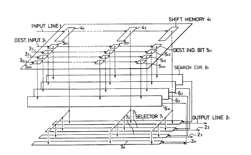
Fig. 1 shows an embodiment of a data queueing apparatus
according to the invention. In the figure, the same
reference designations as used in Fig. 31 are used for
the same or similar parts.
In Fig. 1, an input line 1 receives a limited length
of data and a plurality of output lines 21 - 2~ transmit
data. Destination inputs 31 - 3' are provided
correspondingly to the output lines 21 - 2~ and indicate
destination output ports of received data. Shift
memories 41 - 4k store data. Destination indicating bits
511 - 5~ are provided correspondingly to each shift
memory. The destination indicating bit 51Z, for example,
shows whether the destination of the data stored in the
shift memory 41 is the output line 2Z or not. The
destination indicating bit 5~, for another example, shows
whether the destination of the data stored in the shift
memory 4k is the output line 2v or not. Search circuits
19
CA 02306286 2000-OS-02
61 - 6~ are provided correspondingly to each output lines
21 - 2s. The search circuit 61, for example, is connected
to the destination indicating bits 511. 521 ' ' - 5k1'
Selectors 71 - 7o are provided correspondingly to each of
the output lines 21 - 2.. The selector 71, for example,
corresponding to the output line 21, selects the data to
be transmitted from the shift memories 41 - 4k based on a
search result of the search circuit 61, and transmits the
data selected to the output line 21.
Operation of the apparatus of Fig. 1 is explained
hereinafter. Figs. 2 - 4 show changing signals and
memory contents when the number of the input line 1 is
one, the number m of the output lines 21 - 2' is four, the
number k of the shift memories 41 - 4k is six.
In Figs. 2 - 4, line (a) shows time slots divided by
a fixed length of time. Line (b) shows an example of
data received in the input line 1, and line (c) shows
destination inputs 34, 33, 32, and 31 in this order.
Examples of the contents of the shift memories 41 - 46 and
the destination indicating bits 511 - 564 in each time slot
are shown in lines (d) - (o). Lines (p) - (s) show
examples of the data to be transmitted to the output
lines 21 - 24.
Data received in the input line 1 is a limited
length of information such as frame information divided
CA 02306286 2000-OS-02
into predetermined fixed times, fixed-length address
information, or fixed-length packet information. In
Figs. 2 - 4, the predetermined fixed times are the time
slots and a serial number is assigned to each time slot
from time slot 1 for the convenience of this explanation.
In these figures, one data item is received in each time
slot.
These figures show an example in which no data was
received before the time slot 1 or a long time has passed
since data was last received. and therefore the shift
memories 41 - 46 are empty before time slot 1. One data
item is received in each of the time slots 1, 2, 3, 4, 6,
7, and 8.
In Figs. 2 - 4, the data to be transmitted to the
output lines 21 - 24 are read once every 4 time slots.
Actually, data is read in the time slot 4 and the time
slot 8.
Destination information is received at the
destination inputs 31 - 34 simultaneously with data
received at the input line 1. For example, when the
destination of the received data is the output line 24,
only the destination input 34 is asserted. In the
figures, "1" means an asserted bit, thus, in this case,
destination inputs { 34, 33, 32, 31} become { 1, 0 , 0 , 0 } .
"Data a" addressed to the output line 24 is received
21
CA 02306286 2000-OS-02
in the time slot 1, and "data b" addressed to the output
line 21 is received in the time slot 2. In the time slot
1, the shift memory 46 is empty, thus, "data a" is shifted
to the shift memory 46 immediately. Destination inputs 31
- 34 are stored in the destination indicating bits 564 -
561-
In the same way, in the time slot 2, the shift
memory 45 is empty, thus, "data a" is shifted to the shift
memory 45, and "data b" is shifted to the shift memory 46.
When "data a" is shifted from the shift memory 46 to the
shift memory 45, the destination in the destination
indicating bits 564 - 561 are shifted to the destination
indicating bits 554 - 551 corresponding to the next shift
memory 45.
The following is an explanation of reading out data
to the output lines 21 - 24. Figure 2 shows an example of
transmitting data in the time slot 4. At the first stage
of the time slot 4, the search circuits 61 - 64 search for
and detect data to transmit. When any one of destination
indicating bits 511 - 564 is asserted, a search result to
that effect is passed to the selectors 71 - 74. The
selectors 71 - 74 select one transmitted data of those
detected for each output line 21 - 24 from the shift
memories 41 - 46, and transmit data to the output lines 21
- 24.
22
CA 02306286 2000-OS-02
For example, the search circuit 61 detects data to
transmit to the output line 21. The destination
indicating bits 511. 521' 531' 541' 551' 561 are read in this
order until the asserted bit "1" is detected among these
bits. If the asserted bit is detected, it is passed to
the selector 71. The selector 71 shown in these figures
selects one out of six. The selector 71 selects one of 6
shift memories 41 - 46, and the selected data is
transmitted to the output line 21.
The above operation of transmitting data to the
output line 21 is done independently of transmitting data
to the other output lines 22 - 24. These operations of
transmitting data to the output lines can be done
separately and simultaneously.
The destination indicating bits 511 - 5~ detected by
the search circuits 61 - 64 become deasserted after
selection based on a detection. The data stored in the
shift memories 41 - 46 are deleted after reading. The
next data is shifted to the shift memories 41 - 46, if
there is any data in the previous stage.
The following is a more detailed explanation of the
operation, referring to Figs. 2 - 4.
In each time slot 1 - 4, each of "data a, b, c, and
d" is received. Each of "data a, b, c, and d" is stored
in the shift memories in the order received.
23
CA 02306286 2000-OS-02
In the time slot 4, one data is read and transmitted
to each of the output lines 21 - 24 as described above.
The data to be transmitted to the output line 21 is
explained referring to Fig. 2 hereinafter. In the time
slot 4, the search circuit 61 reads out the destination
indicating bits 511. 521' 531 541' 551 and 561 in this
order. These bits are 0, 0, 0, 0, 1, and 1. The
destination indicating bit 551 is detected from these
values, because it is asserted and read before 561, and it
is passed to the selector 71. The selector 71 selects the
shift memory 45 from six shift memories 41 - 46 based on
the result of the search circuit 6loperation, and "data
b" is transmitted to the output line 21.
When "data b" is transmitted to the output line 21,
the shift memory 45, in which "data b" was stored in the
time slot 4, becomes empty. In the time slot 5, "data
c", which was stored in the previous stage in the time
slot 4, is shifted to the shift memory 45 as shown in Fig.
3. And the destination information in the destination
indicating bits 564. 563' 562' and 561 are also shifted to
the destination indicating bits 554, 553, 552' and 551'
In the same way, "data a" is transmitted to the
output line 24.
Each value of the destination indicating bits 512,
522 ~ 532 ~ 542 ~ 552 ~ and 562, which correspond to the output
24
CA 02306286 2000-OS-02
line 22, is 0, 0, 0, 0, 0, and 0. This means there exists
no asserted hits, thus the search circuit 62 informs the
selector that there is no data to be transmitted. Thus,
no data is transmitted from the output line 22.
In the same way, no data is transmitted from the
output line 23.
No data is received in the time slot 5, however the
data stored in the shift memories are shifted to the next
shift memories. In the time slots 6 - 8, "data e, f, and
g" are received sequentially. The received data are
stored in the shift memories, and then shifted to the
next shift memories.
In the time slot 8, data are read to be transmitted
to the output lines as described above. In this case,
"data c" is detected as the data to be transmitted to the
output line 21 by the search circuit 61. "Data e" is
detected as the data to be transmitted to the output line
22 by the search circuit 6Z. These detected "data c and
e" are transmitted to each output lines. The search
circuits 63 and 64 can know there are no data to be
transmitted to the output lines 23 and 24 because the
destination indicating bits have no asserted bits.
Accordingly, no data is transmitted to the output lines 23
and 24.
In the time slots 9 - 11, no data is received at the
CA 02306286 2000-OS-02
input lines. In these cases, the data stored in the
shift memories are shifted to the next shift memories
sequentially.
"Data d" is stored in the shift memory 41 in the time
slot 10 as shown in Fig. 4. "Data d" cannot be shifted
furthermore because the shift memory 41 is the last stage.
"Data d" remains in the shift memory 41 during the time
slot 11.
This "data d" is detected as the data to be
transmitted to the output line 21 by the search circuit 61
in the time slot 12, then is transmitted to the output
line 21 by the selector 71.
In the above examples, all received data could be
written in the shift memory 46. But data cannot be
written when all of the shift memories 41 - 46 are
occupied by data. In this case, coming data are
discarded. To reduce the possibility of data discard or
loss, the number k of the shift memories 41 - 4k is
desired to be large.
A flow of the above operation is explained
hereinafter referring to Fig.. 5.
At step S1, data and its destination are received at
the input line 1 and the destination inputs 31 - 3a.
At step S2, it is checked whether the first shift
memory, which initially stores the received data, is
26
CA 02306286 2000-OS-02
occupied by any data. When the first shift memory has
been occupied by some other data, the data and the
destination received at step S1, are disposed at step S3.
If it is detected that the first shift memory is empty at
step S2, the first shift memory stores at step S5, the
data and the destination which are received at step S1.
At step S6, it is checked if it is fourth input or
not. When it is not fourth input, the operation from
step S1 - S5 is repeated. While the operation from step
Sl - S6 is repeated, the received data are shifted at
step S6', to the next shift memory one by one. By
forward shifting as described above, the first shift
memory, which receives the data for the first time,
remains empty unless all shift memories are full.
If it is judged to be fourth input at step S6, the
search circuits 61 - 64 search and detect the data to be
transmitted to each output lines by checking the
destination to each output lines at step S7.
At step S8, it is checked if the data to be
transmitted to the output line is detected or not. When
no data is detected to be transmitted, the operation is
repeated from the step S1 again. When any data is
detected to be transmitted at step S8, the data is
selected from the shift memory by the selector at step
S9.
27
CA 02306286 2000-OS-02
At step S10, the data selected by the selector is
transmitted to the corresponding output line.
At step S11, the data is deleted from the shift
memory by clearing the corresponding destination since
the data transmitted at step S10 is no longer needed.
After deleting the data, the operation is repeated from
receiving data and the destination at step S1. And the
data stored in the previous shift memory is requested to
shift to the next stage by this data deletion. Thus, the
data stored in the previous shift memory is overwritten
in the shift memory where the destination has been
cleared.(Step S6')
As described above, in this embodiment, received
limited-length data in the input line 1 are written in
the shif t memories, in which data can be shifted from one
to the next sequentially regardless of its destination.
The destination indicating bits are associated with each
of the shift memories. The search circuits search the
data to be transmitted in received order by detecting an
asserted bit from the destination indicating bits
corresponding to the destination output lines, and the
data is extracted by the selectors. After extraction,
the selector transfers the data to the desired output
lines and the previous data is shifted to overwrite the
transmitted data.
28
CA 02306286 2000-OS-02
By this embodiment, the data received at the input
line is written in the shift memories and its destination
is stored in the destination indicating bits. Data are
read in arrival order by searching the destination
indicating bits corresponding to each of the output
lines, so that the received data can be transmitted to
the desired output line in arrival order. The shift
memories can be used commonly for all output lines, so
that the data queueing apparatus can reduce the
possibility of data loss, which would be caused by
attempting to write data, especially receiving bursty
data which exceed the capacity of the shift memories.
Embodiment 2.
The following is an explanation of another
embodiment of this invention referring to the drawings.
Fig. 6 shows another embodiment of the data queueing
apparatus according to this invention. The same
reference designations are used for the same or similar
elements as in Embodiment 1 and are not explained here,
for clarity sake.
In Fig. 6, shift detectors 81 - 8k are provided
correspondingly to each shift memories 41 - 4k. The shift
detectors trigger shifting of data stored in the previous
shift memories 41- 4k when they detect the case that none
of m number of destination indicating bits are asserted.
29
CA 02306286 2000-OS-02
For example, when the shift detector 82, provided
correspondingly to the shift memory 42, detects that none
of destination indicating bits 521. 522...52 are asserted,
it shifts data stored in the previous shift memory 43.
Operation of this embodiment is explained
hereinafter. Figs. 7 - 9 are charts which show each
signal and changing status of each element. In this
case, the number of the input lines 1 is one, the number
m of output lines 21 - 2~ is four, and the number k of
shift memories 41 - 4k is six.
In Figs. 7 - 9, line (a) shows time slots, line (b)
shows an example of data received at the input line 1,
and line (c) shows each of the destination inputs 34, 33,
32, and 31 for indicating the destination of the received
data in this order. Lines (d) - (u) show examples of the
status of the shift memories 41 - 46 and the destination
indicating bits 511 - 5~ in each time slot. And lines (v)
- (y) show the data to be transmitted to each of the
output lines 21 - 2Q.
The data received at the input line 1 is limited-
length information such as frame information divided by a
predefined fixed time, fixed length address information,
or fixed length packet. In Figs. 7 - 9, the fixed-length
time is defined as a time slot. As shown in line (a), a
serial number is assigned sequentially from time slot 1
CA 02306286 2000-OS-02
for purposes of this explanation. In these figures, one
data item is received in one time slot.
These figures show an example in which no data was
received before the time slot 1 or a long time has passed
since the last data was received, and the shift memories
41 - 46 therefore store no data gust prior to the time
slot 1. One data item is received in each of the time
slots 1, 2, 3, 4, 6, 7, 8, 9, and 11.
In Figs. 7 - 9, the data to be transmitted to the
output lines 21 - 24 are read out once every 4 time slots.
Actually, data is read out in the time slot 4, in the
time slot 8 and the time slot 12.
Destination information is received at the
destination inputs 31 - 34 simultaneously with data
received at the input line 1. For example, when the
destination of the received "data h" is the output line
24, the destination input 34 becomes asserted. In the
figures, "1" means an asserted bit, thus, in this case,
the destination inputs {34, 33, 32, 31} become {1, 0, 0,
0}.
When the received data is destined for a plurality
of output lines, that is, multicast data, a plurality of
bits of the destination inputs 31 - 34 become asserted.
For example, "data a" received in the time slot 1 is
addressed to the output Lines 21 and 24, thus the
31
CA 02306286 2000-OS-02
destination inputs 31 and 34 become asserted. In other
words, the destination inputs {34, 33, 32, 31} become {1,
0, 0, 1}.
In the time slot 1. "data a" addressed to the output
lines 21 and 24 is received, and "data b" addressed to the
output line 22 is received in the time slot 2. In the
time slot 1, the shift memory 46 is empty. "Data a" is
therefore shifted to the shift memory 46 immediately. The
destination inputs 31 - 34 are stored in the destination
indicating bits 564 - 561'
In the same way, in the time slot 2, the shift
memory 45 is empty. Therefore, "data a" is shifted to the
shift memory 45, and "data b" is shifted to the shift
memory 46. With shifting "data a" from the shift memory
46 to 45, the destination in the destination indicating
bits 564 - 561 are simultaneously shifted to the
destination indicating bits 5~4 - 551, which are provided
correspondingly to the next shift memory 45.
The shift detectors 81 - 86 are provided
correspondingly to the shift memories 41 - 46. In the
time slot 1, they detect the case that none of m number
of the destination indication among the destination
indicating bits 511 - 564 is asserted. For example, in the
figures, as a status value of the shift detector, "1" is
defined as meaning that at least one of the destination
32
CA 02306286 2000-OS-02
indicating bits is asserted, and "0" is defined that
there is no asserted bit among the corresponding
destination indicating bits. Given this definition, OR
gates can be used for the shift detectors 81 - 86.
For example, all of the destination indicating bits
561 - 564 corresponding to the shift memory 46 are "0" in
the time slot 1, thus the status of the shift detector 86
becomes "0". In the time slot 2, one of the destination
indicating bits 561 - 5~ corresponding to the shift memory
46 is "1", thus the status of the shift detector 86
becomes "1".
The following is an explanation of reading out data
to be transmitted to the output lines 21 - 24.
Fig. 7 shows an example of transmitting data in the
time slot 4. At a first stage of the time slot 4, the
search circuits 61 - 64 search for and detect data to be
transmitted. When any one of the destination indicating
bits 511 - 5~ is asserted, it is communicated to the
corresponding selectors 71 - 74. The selectors 71 - 74
select one from the shift memories 41 - 46, and transfer
data to the output lines 21 - 24.
For example, the search circuit 61 detects data to be
transmitted to the output line 21. The destination
indicating bits 511. 521' 531' 541 551' 561 are read in this
order until the asserted bit "1" is detected among these
33
CA 02306286 2000-OS-02
bits. If the asserted bit is detected, it is
communicated to the selector 71. The selector 71 in the
figure is a selector which selects one from six. The
selector 71 selects one from six shift memories 41 - 46,
and the selected data is transferred to the output line
21.
An operation of transmitting data to the output line
21 is carried out independently of transmitting data to
the other output lines 2Z - 24. These operations can be
done separately and simultaneously.
The destination indicating bits 511 - 564 detected by
the search circuits 61 - 64 are updated and become
deasserted after selection of the corresponding data for
transmit based on a detection. Then, each of the shift
detectors 81 - 86 detect the possibility of shifting data
to each of the corresponding shift memories 41 - 46 based
on the updated destination indicating bits 511 - 564. When
it is noticed to be possible to shift data and the
previous shif t memory is occupied by data, the data is
shifted to the corresponding shift memory.
The data to be transmitted to the output line 21 is
explained referring to the figures hereinafter. In the
time slot 4, the search circuit 61 reads out the
destination indicating bits 511, 5Z1, 531, 541 551 and 5g1
in this order. Each value of these bits is 0, 0, 0, 1,
34
CA 02306286 2000-OS-02
0, and 1. The asserted destination indicating bit 541 is
detected from these values, and it is communicated to the
selector ?1. The selector ?1 selects the shift memory 44
from six shift memories 41 - 46 based on the detection by
the search circuit 61, and "data a" is transmitted to the
output line 21.
After "data a" is transferred to the output line 21,
the corresponding destination indicating bit 541 is
cleared or deasserted.
In the same way, the search circuit 64 detects "data
a" stored in the shift memory 44 as the data to be
transferred to the output line 24 in the time slot 4.
After "data a" is transferred to the output line 24, the
corresponding destination indicating bit 544 is cleared or
deasserted.
In the time slot 4, the destination indicating bits
{5,~, 543, 542' 541} corresponding to the shift memory 44,
which stored "data a", change value from {1, 0, 0, 1} to
{0, 0, 0, 0}. The shift detector 84 also changes status
value from "1" to "0" at the same time.
When the shift detector 84 changes the status value
from "1" to "0", that means "data a" is transmitted to
all of the desired destinations, that is, the output
lines 21 and 24. Then, "data a" is deleted.
In the same way, "data b" in the shift memory 45is
CA 02306286 2000-OS-02
transmitted to the output line 22 in the time slot 4.
"Data c" stored in the previous shift memory 46 is shifted
to the shift memory 45 in the time slot 5. And each of
the destination indicating bits 564, 563, 562~ and 561 is
also shifted to each of the destination indicating bits
554, 553, 552' and 551 with shifting "data c" simultaneously.
Each of the destination indicating bits 513, 523 533
543 ~ 553 ~ and 563, which correspond to the output line 23,
is 0, 0, 0, 0, 0, and 0. This means there exists no
l0 asserted bits, thus the search circuit 62 communicates the
selector that there is no data to transmit. No data is
transmitted from the output line 23.
In the time slot S, no data is received. "Data e,
f, and g" are received in the time slots 6 - 8.
In the time slot 8, the search circuit detects the
data to transmit. In this case, "data c" is to be
transmitted to the output line 21. "Data d" is to be
transmitted to the output line 22. Though "data d" is
multicast data addressed to the output lines 21 and 22,
"data c" is already chosen to be transmitted to the
output line 21. Thus, "data d" is transmitted only to the
output line 22. "Data e" is multicast data addressed to
all output lines. But each of "data c and d" is already
detected as the data to be transmitted to each of the
output lines 21 and 22 in this case. "Data e" is thus
36
CA 02306286 2000-OS-02
transmitted to the output lines 23 and 24.
As a result, all of the destination indicating bits
of "data c" become "0" and the shift detector changes the
status value from "1" to "0". On the other hand, some of
the destination indicating bits of "data d" and "data e"
are still asserted, so that the status value of the shift
detectors remain "1".
In the time slot 9, "data h" is received and no data
is received in the time slot 10.
"Data d", stored in the shift memory 41 in the time
slot 10, cannot be shifted further because the shift
memory 41 is the last stage, so that "data d" remains in
the shift memory 41 in the time slot 11.
This "data d" is transmitted to the output line 21 in
the time slot 12. After "data d" is transmitted to the
output line 21, no destination indicating bits are
asserted, so that the shift detector changes the status
value from "1" to "0". Thus. "data d" is deleted.
In the above examples, all received data can be
written in the shift memory 46. But received data cannot
be written when all of the shift memories 41 - 46 are
occupied by data. In this case, coming data are
discarded. To reduce the possibility of data discard or
loss, the number k of the shift memories 41 - 4k is
desired to be large.
37
CA 02306286 2000-OS-02
As described above, in this embodiment, if multicast
data addressed to a plurality of the output lines is
received, the data can be shifted from one shift memory
to the next, in accordance with whether the shift
detectors detect that the data is transmitted to all
desired output lines indicated by the destination
indicating bits. The received data can be transmitted to
the desired output line in the received order. The shift
memories are each common to all output lines, so that the
data queueing apparatus can reduce the possibility of
data loss, which would be caused by attempting to write
data, especially receiving bursty data which exceed the
capacity of the shift memories.
In this embodiment, the multicast data can be stored
in the shift memories until the data is transmitted to
all desired output lines, so that multicast processing
can be done even if the shift memories are used commonly
by all output lines.
Embodiment 3.
In the above embodiments 1 and 2, the number of
input lines is one. The data queueing apparatus can be
also configured for writing a plurality of data in
parallel from a plurality of input lines la, lb and lc.
In Fig. I0, (a) shows an example of this embodiment.
In the figure, the shift memories 41 - 49 are provided.
38
CA 02306286 2000-OS-02
The data is received at each of the input lines la, lb,
and lc to each of the shift memories 47, 48, and 49. In
the same way, each of the destination inputs is stored in
each of the destination indicating bits. In this
example, the number of input lines is three and therefore
three received data can be written in the shift memories
in parallel simultaneously. In this configuration, three
shift memories store received data simultaneously as
shown in Fig. 10 (b), therefore the apparatus shifts the
data three times in one time slot. Namely, the apparatus
is configured to receive data and to shift data three
times in one time slot. In this embodiment, though the
shift memory has to shift the data more quickly than
Embodiments 1 and 2, the data can be received in the
plurality of input lines to be processed simultaneously,
so that a large amount of data can be processed at a high
speed.
Embodiment 4.
In the above Embodiments 1 and 2, the search
ZO circuits are provided correspondingly to the output lines
and the search circuits operate independently and
simultaneously. But a data queueing apparatus can be
also configured with fewer search circuits, each of which
corresponds to a plurality of output lines. The search
circuits operate at a high speed and each search circuit
39
CA 02306286 2000-OS-02
detects the data stored in the plurality of shift
memories, so that the scale of the hardware can be
reduced.
Fig. 11 shows an example of this embodiment. In the
figure, the search circuit 61 is provided correspondingly
to the output lines 21 and 22, and the search circuit 62
is provided correspondingly to the output lines 23~and 24.
Namely, one search circuit is provided correspondingly to
two output lines. The search circuits 61 and 62operate
at more than two times the speed of the search circuits
in Embodiments 1 and 2, so that the same effect can be
attained as in Embodiments 1 and 2.
Another case where only one search circuit is
provided is possible (not shown in a figure). In this
case, one search circuit is provided for the output lines
21 - 24, so that the search circuit needs to operate at
more than four times the speed of the search circuits in
Embodiments 1 and 2. The search circuit can be common in
this case, and therefore the apparatus scale can be
reduced.
Embodiment 5.
In Embodiments 1 and 2, the shift memories shift the
data one by one in one time slot, but it is desirable
that the shifting speed is higher. The apparatus of this
embodiment is configured as the same as in Embodiments 1
CA 02306286 2000-OS-02
and 2, however, it shifts data asynchronous with the time
slot. That is, the interval of shiftings is shorter than
the period of the time slot. The speed of shifting data
is increased, and data can be shifted forward more
quickly. Thus, the received data is stored certainly in
the shift memory.
Embodiment 6.
In the above embodiments, the data is read once
every four time slots, but in another case, for example,
the data can be read once every time slot. This reading-
out frequency can be vary.
Embodiment 7.
In the above embodiments, the speed of the input
lines is the same as the speed of the output lines.
However, a higher traffic concentration can be achieved
by reading the data from the shift memory at a higher
speed. It is also possible that the data can be written
from the input line at a higher speed than it is read out
at the output lines.
Embodiment 8.
In the above embodiments, a set of the destination
indicating bits and a search circuit are provided
correspondingly to each of the output lines of the data
queueing apparatus. A plurality of the above sets of the
destination indicating bits and search circuits may be
41
CA 02306286 2000-OS-02
provided correspondingly to each of the delay priorities.
The data having higher delay priority can be read first
based on a code, which indicates the delay priority.
Fig. 12 shows an example of this embodiment. In the
figure, a header converter 17, a first queueing apparatus
100, and a second queueing apparatus 200 are provided.
In Fig. 12, two sets of the data queueing apparatuses are
provided for one output line. The header converter 17
detects the delay priority included in the header of the
received data. The data are distributed to the first
queueing apparatus or the second queueing apparatus based
on the delay priority. The first queueing apparatus is
configured to have higher priority than the second
queueing apparatus. For example, the first queueing
apparatus may read the data once every four time slots
and the second queueing apparatus may read the data once
every eight time slots. By making such a difference
between two queueing apparatuses, the priority of the
first queueing apparatus becomes higher than the second
queueing apparatus. Higher priority of the first
queueing apparatus can also be got by reading the data in
the second queueing apparatus after all data in the first
queueing apparatus have been read.
Embodiment 9.
Fig. 13 shows another embodiment of this invention
42
CA 02306286 2000-OS-02
using priority. In this embodiment, priority can be
controlled by indicating the destination with two bits
instead of one bit. A priority table 30 and a count
table 31 are included in the header converter 17 as shown
in Fig. 13.
The priority table is a table showing a priority
corresponding to two bits as shown in Fig. 14. The count
table is a table for counting how many data items with
different priorities are stored in the shift memories
corresponding to each output lines, as shown in Fig. 15.
The header converter 17 receives the data having one
of "high", "middle", "low" priorities and transmits it to
the shift memory. The header converter 17 sets the value
for each of destination indicating bits corresponding to
the received priority. When the value of the bits is
"00", no data exists. In other cases, the value of the
bit is set correspondingly to each priority. The header
converter 17 sets the priority with reference to the
priority table 30.
The header converter 17 also increments the
corresponding value of the count table 31 when the data
and the destination indication is transmitted to the
first shift memory. The count table shows how many data
items, having each of priorities, exist for each of the
output lines. The search circuit searches for and
43
CA 02306286 2000-OS-02
detects the data to be transferred to each of the output
lines in an order of priority with reference to this
count table. For example, the search circuit 61 is
informed that one data having "high" priority and one
data having "middle" priority exist by the count table 31
as shown in Fig. 15. The search circuit detects the data
having "high" priority and requests to the selector to
select and transfer it first. For example, in Fig. 13,
the data having "high" priority is stored in the shift
memory 4z, so that the selector 71 selects and transfers
the data stored in the shift memory 42 earlier than the
data having "middle" priority stored in the shift memory
41 to the output line 21.
In this way, priority control can be processed by
using plural bits in .the destination indicating bits
which show the priority of the data.
Embodiment 10.
Furthermore, in the above embodiment, the data can
be processed as a parallel signal by providing a serial-
parallel converter and/or a parallel-serial converter in
the pre-stage and/or the post-stage of the data queueing
apparatus, if the operation speed is limited in the data
queueing apparatus.
Fig. 16 shows this embodiment. In this case, the
number of the input lines ly is eight. In this
44
CA 02306286 2000-OS-02
embodiment, the shift memory is configured to have eight
bits and the input lines are provided correspondingly to
each of bits, so that eight bits can be written in the
shift memories in parallel. In this way, data transfer
at a higher speed can be achieved by providing a
plurality of the input lines compared with the case of
one input line.
Embodiment 11.
In the above Embodiments 1 and 2, the limited-length
data is received. The data can be address information in
the packet switch, or the packet itself. Also other
kinds of data can be processed with the apparatus
described in the above Embodiments 1 and 2.
Embodiment 12.
In the above Embodiments 1 and 2, the shift memories
and the destination indicating bits are configured as
different memories. But the same memory unit can be used
for the shift memories and the destination indicating
bits as shown in Fig. 17. For example, when the shift
memory has eight bits and the destination indicating bits
have four bits, twelve bits are combined as one memory
unit. The received data and the destination inputs can
be stored by the memory unit of twelve bits.
Embodiment 13.
The above Embodiments 1 and 2 show the apparatus in
CA 02306286 2000-OS-02
which the selectors are provided correspondingly to each
output lines, but another apparatus can be configured
with fewer selectors. For example, each selector may
correspond to two output lines as shown in Fig. 18. In
this embodiment, the selectors operate at twice the speed
of the selectors in Embodiments 1 and 2, achieving the
same effect as in the above embodiments can be attained.
Embodiment 14.
The above Embodiment 4 and 13 show the apparatus in
which the numbers of the search circuits and the
selectors can be reduced by operating the search circuits
and the selectors at a high speed. The numbers of the
search circuits and the selectors can also be reduced
even if they do not operate at a high speed as follows.
Fig. 19 shows the operation of the apparatus as
configured as shown in Fig. 18. In the above Embodiments
1 and 2 (also in Embodiment 4 and 13), the data is
transmitted every 4 time slots, but this embodiment shows
the case in which the data is transmitted every time
slot. The search circuit 61 searches and detects the
existence of the data to be transferred to the output
lines 21 and 22 alternately every time slot. The selector
71 also transmits the data, if there is any, to the output
lines 2land 22 alternately every time slot. In this way,
the search circuit and the selector do not need to
46
CA 02306286 2000-OS-02
operate at a high speed while detecting and transmitting
the data every time slot. In Fig. 19, more effective
operation can be achieved. The apparatus in this
embodiment can transmit data every time slot, not every
fourth slot, even if it operates at the same speed as in
Embodiments 1 and 2.
Embodiment 15.
Another apparatus can be provided using one search
circuit and one selector as shown in Fig. 20. In this
case, if the search circuit 6 and the selector 7 operate
at four times the speed of the search circuits in
Embodiments 1 and 2, the same effect can be attained as
in the above embodiments.
Embodiment 16.
Fig. 21 shows the operation of the apparatus
configured as shown in Fig. 20, but in this case, the
search circuit and the selector operate at the same speed
as in Embodiments 1 and 2.
The search circuit detects and the selector
transmits the data to be transferred to each output line
once every time slot in the case shown in Fig. 21.
Therefore, the same effect can be attained by detecting
and selecting the data to be transferred to each output
line once every time slot. In this case, the apparatus
needs only one search circuit 6 and one selector 7, in
47
CA 02306286 2000-OS-02
addition, they do not need to operate at a high speed, so
that the circuits are simply configured.
Embodiment 17.
Fig. 22 shows an example of a shared multibuffer ATM
switch. This shared multibuffer ATM switch is
characterized by adopting in the controller 16 the data
queueing apparatus 180 described above.
Fig. 23 shows a configuration of the data queueing
apparatus 180. The data queueing apparatus 180 has the
same function as the data queueing apparatus described in
Embodiment 1. Flags correspond to the above-described
destination indicating bits which store the destination
information. Address corresponds to the data stored in
the above-described shift memories. And a searching
element corresponds to the above-described search
circuit.
Fig. 24 shows a shift operation. The value of an
occupation indicator becomes "0" when all of the flags
are "0". When the occupation indicator indicates "0",
the data stored in the previous stage is shifted to the
next.
Fig. 25 explains the forward shifting shown in Fig.
24. In the first stage, the flags have been set 1, 0, 0,
so that the occupation indicator indicates "1" as shown
in Fig. 25. The value of the occupation indicator is
48
CA 02306286 2000-OS-02
transmitted to a shift trigger of the second stage. The
shift trigger shifts the data which are stored in the
stage where the shift trigger exists, to the next stage
when the value of the occupation indicator becomes "0".
In the second stage, the flags are all "0", so that the
occupation indicator indicates "0". The shift trigger of
the third stage shifts the address and the destination
indication, stored in the third stage, to the second
stage.
Fig. 26 is a graph comparing the memory size needed
by the conventional data queueing apparatus and by the
data queueing apparatus according to this embodiment. In
Fig. 26, the horizontal axis shows the number of the
output lines and the vertical axis shows the ratio of the
memory size needed by the apparatus according to this
embodiment to the memory size needed by the conventional
apparatus. The graph shown in Fig. 26 is made using the
formula as shown in Fig. 27. As shown in Fig. 26, the
more output ports the apparatus has, the smaller memory
size is needed by the data queueing apparatus of this
embodiment compared with the conventional apparatus.
Embodiment 18.
Fig. 28 shows another embodiment for shifting the
data stored in the shift memories. In the above
embodiments, the data-stored in the shift memories are
49
CA 02306286 2000-OS-02
shifted forward once every time slot. It is desirable to
shift the stored data a plurality of times every time
slot as shown in Fig. 28, not to shift data once every
time slot. In this case, data are received every time
slot, and the received data can be certainly stored in
the shift memories by previously shifting forward the
stored data.
Embodiment 19.
Fig. 29 shows another example of the searching
element. In the above embodiment, the searching element
is provided correspondingly to each output line. In this
embodiment, the searching element is provided in common
for a plurality of the output lines. A switch 60 is
provided for the searching element, and the switch
changes the connections with the flags for searching each
flag sequentially. In this case, the searching element
may operate at a high speed, or the searching element may
not operate a,t a high speed for searching the data to be
transmitted to each output line once every time slot. In
this embodiment, the same effect can be attained as in
the above embodiments.
Embodiment 20.
Each of the flags is not needed to be 1 bit, but it
can consist of 2 or more bits, not shown in the figure.
When a flag has 2 or more bits, the priorities of the
CA 02306286 2000-OS-02
data can be processed.
The invention has been described in connection with
a number of specific embodiments. These embodiments are
given by way of example only, and the scope of the
invention is limited only by the scope of the appended
claims.
51