Note: Descriptions are shown in the official language in which they were submitted.
CA 02306649 2000-04-25
OPTICAL ADDRESS DECODER
FIELD AND BACKGROUND OF THE INVENTION
The present invention relates to optical data transmission and, more
particularly, to an optical data packet address decoder and corresponding
address
formats.
There are two kinds of digital communications networks in common use:
to electronic and optical. Optical data transmission has the advantage over
electronic
data transmission of relative immunity to interference and crosstalk and a
significantly
higher bandwidth. For several messages to share the same physical
communications
channel, the messages must be multiplexed. Several multiplexing schemes are
commonly used in electronic networks, including time division multiplexing
(TDM),
frequency division multiplexing (FDM) and code division multiplexing (CDM).
FDM is straightforward to implement in an optical network, where it is also
commonly referred to as "wavelength division multiplexing" (WDM): each message
is assigned its own carrier wavelength, and simple wavelength-sensitive
optical
components such as diffraction gratings are used to sort out the different
messages.
2o Several papers were presented at the 1998 Conference on Lasers and Electro-
Optics
(San Francisco CA, May 3-8) on optical TDM and CDM implementations.
In both electronic and optical networks, all but the shortest messages are
transmitted as several discrete packets, according to a variety of well-known
protocols
such as TCP/IP. Figure 1 shows a typical format of a data packet 10: an
address block
14, which indicates the destination of data packet 10 by having a destination
address
encoded therein, followed by a data block 12 wherein the portion of the
message
CA 02306649 2000-04-25
2
contained in data packet 10 is encoded. The convention in Figure 1, and in
other
Figures below, is that data packets are transmitted from left to right, so
that, for
example, address block 14 reaches a destination node in a network before data
block
12. Both the address and the message are encoded digitally, as sequences of
regularly
spaced electronic or optical pulses, with, for example, the presence of a
pulse
indicating a binary 1 and the absence of a pulse indicating a binary 0. The
first bit of
address block 14 is on the right side of address block 14, followed by the
rest of the
bits of address block 14, and similarly for data block 12. Both address block
14 and
data block 12 have fixed and known transmission times. Typically, address
block 14
1o and data block 12 both are formatted with a fixed number of bits, and their
transmission times are the number of bits multiplied by the time interval
associated
with one bit; but, as will be seen below, other address block formats are
possible.
Typically, there is a time delay between the end of address block 14 and the
beginning
of data block 12.
SUMMARY OF THE INVENTION
Figure 2 is a block diagram of an optical address decoding system 20, of
which the device of the present invention is one component. Single arrows
indicate
the flow of optical data. Double arrows indicate the flow of electronic data.
System
2o 20 enables the implementation of time division multiplexing in an optical
transmission network. A data packet 10 enters system 20 from an input channel
34.
A 1 x 2 switch 22 diverts address block 14 to the left branch of Figure 2 and
data
block 12 to the right branch of Figure 2. Address block 14 is decoded in a
decoder 24.
According to the decoded address, an electronic signal is sent to a switch
control 33
CA 02306649 2000-04-25
3
- instructing switch control 33 to set a switch array 32 to direct data packet
10 to one of
a plurality of output channels 36. Because the decoding process in decoder 24
destroys, or at least rearranges, address block 14; the decoded address is
sent to an
address restoration unit 26 which reconstructs address block 14. Depending on
the
type of optical network, the reconstructed address block 14 may or may not be
identical to address block 14 that was input to decoder 24. Meanwhile, data
block 12
is transmitted along the right branch of Figure 2. Optionally, a delay unit 30
is
provided to retard the transmission of data block 12 for the amount of time
needed to
decode and reconstruct address block 14, to preserve the built-in delay
between
1o address block 14 and data block 12. Finally, address block 14 and data
block 12
merge to reconstruct data packet 10, which enters switch array 32 and then
exits
switch array 32 along the appropriate output channel 36. The device of the
present
invention is an improved embodiment of decoder 24.
Therefore, according to the present invention there is provided a device for
decoding an address block, of an optical data packet, wherein is encoded one
of a
plurality of addresses, including: (a) a plurality of waveguides; (b) a
splitting
mechanism for directing the address block simultaneously to each of the
waveguides;
and (c) for each of the waveguides, a detector for detecting light propagating
in the
each waveguide.
Furthermore, according to the present invention there is provided a method of
routing optical data packets, including the steps of: (a) providing each data
packet
with an address block wherein is encoded one of a plurality of addresses; (b)
providing a plurality of waveguides; (c) directing the address block
simultaneously to
each of the waveguides; (d) detecting an intensity of light propagating in
each the
CA 02306649 2000-04-25
4
' waveguide as a result of the directing of the address block to each the
waveguide; and
(e) inferring the address from at least one of the intensities.
The device of the present invention simultaneously directs address block 14 to
a plurality of waveguides. Each waveguide terminates in a detector. The
physical
properties of each waveguide, for example, the length of each waveguide,
determine
the propagation characteristics of the light in the waveguide. Each waveguide
is
configured so that the light is propagated within each waveguide in a manner
unique
to that waveguide. For example, if the waveguides have different lengths, a
particular
pulse of address block 14 reaches the detectors at different times. The
address
to encoded in address block 14 is inferred from the pattern of activation of
the detectors
by the light propagating in the waveguides.
Like WDM, the method of the present invention is compatible with
communications protocols that have low synchronicity requirements. However,
the
present invention supports TDM, and can be used to implement a variety of
transmission modes, such as ATM (asynchronous transmission mode).
According to one preferred embodiment of the present invention, the
waveguides are configured as resonant cavities. The address formatting
appropriate to
this embodiment is a series of equally spaced pulses, with the address encoded
as the
pulse spacing. Each cavity resonates at a different pulse spacing. Only the
detector
2o whose waveguide resonates in response to a particular address block 14 is
activated.
According to another preferred embodiment of the present invention, the
address is formatted conventionally, as regularly spaced bits, and the length
difference
between successive waveguides is the distance that light propagates in the
waveguides
during the time interval associated with one bit. The outputs from the
detectors are
CA 02306649 2000-04-25
S
directed, with equal delays, to individual gates of appropriately configured
gate
arrays, so that only one gate array, corresponding to a particular address, is
activated
by a particular address bloc~C 14.
BRIEF DESCRIPTION OF THE DRAWINGS
The invention is herein described, by way of example only, with reference to
the accompanying drawings, wherein:
FIG. 1 shows the format of an optical data packet;
FIG. 2 is a block diagram of an optical address decoding system;
1o FIG. 3 illustrates a first variant of a first preferred embodiment of the
decoder
of the present invention;
FIG. 4 illustrates a second variant of the first preferred embodiment of the
decoder of the present invention;
FIG. 5 illustrates a second preferred embodiment of the decoder of the present
I S invention.
DESCRIPTION OF THE PREFERRED EMBODIMENTS
The present invention is of an optical address decoder, and associated
methodology, which can be used to implement TDM or ATM in an optical data
2o communications network.
The principles and operation of optical address decoding according to the
present invention may be better understood with reference to the drawings and
the
accompanying description.
CA 02306649 2000-04-25
6
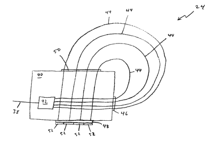
Referring again to the drawings, Figure 3 illustrates a first variant of a
first
preferred embodiment of decoder 24 of the present invention. This embodiment
of
decoder 24 is based on four waveguides 44, which are partly fabricated on an
integrated optics chip 40 by standard methods and partly implemented outside
chip 40
as optical fibers. An input waveguide 38 introduces incoming optical signals
to a
multimode interference splitter 42, which splits the signals among waveguides
44.
Waveguides 44 leave chip 40 at a semireflective layer 46 and return to chip 40
at an
antireflective layer 50. Each waveguide 44 is coupled to a corresponding
optoelectronic detector 52 at another semireflective layer 48. Each
optoelectronic
detector 52 produces a voltage that is proportional to the intensity of the
light incident
thereon. Note that waveguides 44 all are of different lengths. Semireflective
layers
46 and 48 define, in each waveguide 44, a resonant cavity, each resonant
cavity being
of a different length. Not shown in Figure 3 is the processing electronics
associated
with detectors 52. Only four waveguides 44 are shown in Figure 3 for
illustrational
simplicity. A more typical number of waveguides 44 is between 8 and 16.
The use of multimode interference splitter 42 in decoder 24 to split the
incoming signals among waveguides 44 is illustrative, not obligatory. Other
kinds of
optical components, for example, a cascaded y-sputter, may be used for this
purpose.
The basic address format appropriate to decoder 24 of Figure 3 is a sequence
of equally spaced optical pulses, with the destination address represented by
the
spacing between pulses. The lengths of the resonant cavities are chosen so
that the
optical path length in each resonant cavity is an integral or half integral
multiple of
the optical path distance traveled by the light in waveguides 44 during the
time
corresponding to one interpulse spacing of one of the addresses. For a given
address,
CA 02306649 2000-04-25
7
as each pulse enters the resonant cavities, it is partly reflected at
semireflective layers
46 and 48. In the resonant cavity whose optical path length corresponds to the
interpulse spacing of the given address, successive pulses coincide and
reinforce each
other inside the resonant cavity. In the other resonant cavities, successive
pulses do
not coincide and do not reinforce each other. Detectors 52 are selected to
have
response times on the order of the pulse widths. The signal produced by the
detector
52, associated with the resonant cavity whose optical path length corresponds
to the
interpulse spacing of the given address, has a periodicity related to the
interpulse
spacing and a maximum value significantly greater than the signal produced by
one
1o pulse. The signals produced by the other detectors 52 have no such
periodicity and
have maxima on the order of the signal produced by one pulse. The processing
electronics associated with detectors 52 monitors the signals produced by
detectors 52
and identifies which of detectors 52 is producing signals characteristic of
resonance.
The address associated with this detector is the address that is encoded in
address
block 14 that entered decoder 24 of Figure 3 via input waveguide 38.
For example, in a 10 GHz optical data transmission network, with pulses
whose duration is on the order of 0.1 nanoseconds, seven different addresses
can be
encoded as trains of pulses with seven different interpulse spacings on the
order of 2
nanoseconds, corresponding to address frequencies on the order of 500 MHz,
with 20
2o MHz spacings between the address frequencies. The following table shows
feasible
address frequencies and corresponding resonant cavity lengths for waveguides
44
made of silica and carrying light of wavelength 1550 nm, at which wavelength
the
index of refraction of silica is about 1.5. The lengths shown correspond to
two
interpulse spacings.
CA 02306649 2000-04-25
8
channel address frequency (MHz) cavity length (mm)
1 440 227
2 460 217
3 480 208
4 500 200
520 192
6 540 185
7 560 178.
Conventional methods of fabricating integrated optics chips are sufficiently
accurate, geometrically, to give waveguides 44 the proper lengths with respect
to
pulse timing. Nevertheless, higher accuracy than this is needed to ensure that
s overlapping pulses actually reinforce each other and do not interfere
destructively. It
is necessary that overlapping pulses be in phase with each other, preferably
to within
about one degree of phase. To achieve this level of accuracy requires active
tuning of
the indices of refraction of the portions of waveguides 44 that lie on chip
40. These
indices of refraction may be modulated thermally in thermo-optic materials
such as
to silica and ion glass, or electronically in electro-optic materials such as
lithium niobate
and gallium arsenide.
In a more sophisticated addressing scheme, some addresses are associated with
superpositions of several sequences of equally spaced pulses, each sequence
with a
slightly different interpulse spacing. Under this scheme, these addresses
produces
resonance conditions in two or more resonant cavities, and trigger resonance
condition responses in two or more detectors 52. Under this scheme, the four
waveguide 44 embodiment of Figure 3 accommodates fifteen different addresses.
CA 02306649 2000-04-25
9
Figure 4 illustrates a second variant of the first preferred embodiment of
decoder 24 of the present invention, suitable for higher frequency
communications
than the variant of Figure 3. Unlike t~e variant of Figure 3, the variant of
Figure 4 has
waveguides 60 thereof fabricated entirely on an integrated optics chip 56. As
in the
case of the variant of Figure 3, an input waveguide 54 leads to a multimode
interference sputter 58 which splits incoming optical signals among waveguides
60.
Each waveguide 60 is coupled to a corresponding optoelectronic detector 66 at
a
semireflective layer 64. Each waveguide 60 is provided with a semireflective
trench
minor 62, thereby defining, between that trench mirror 62 and semireflective
layer 64,
a resonant cavity. Trench minors 62 are positioned at different distances from
semireflective layer 64, so that the resonant cavities all have different
lengths. As in
Figure 3, the processing electronics associated with detectors 66 is not
shown. Only
four waveguides 60 are shown in Figure 4 for illustrational simplicity. A more
typical
number of waveguides 60 is between 8 and 16.
The variant of Figure 4 functions substantially the same as the variant of
Figure 3, but at a higher frequency. For example, in a 50 GHz optical data
transmission network, with pulses whose duration is on the order of 0.02
nanoseconds, seven different addresses can be encoded as trains of pulses with
seven
different interpulse spacings on the order of 0.5 nanoseconds, corresponding
to
2o address frequencies on the order of 2 GHz, with 50 MHz spacings between the
address frequencies. The following table shows feasible address frequencies
and
corresponding resonant cavity lengths for waveguides 60 made of lithium
niobate and
carrying light of wavelength 1550 nm, at which wavelength the index of
refraction of
CA 02306649 2000-04-25
lithium niobate is about 2.15. As in the case of the variant of Figure 3, the
lengths
shown correspond to two interpulse spacings.
channel address frequency (GHz) cavity length (mm)
1 2.15 32.6
2 2.10 33.3
3 2.05 34.1
4 2.00 35.0
5 1.95 - . 35.9 __._. ..
6 1.90 36.8
7 1.85 37.8
Figure 5 illustrates the second preferred embodiment of decoder 24 of the
5 present invention. As in the embodiment of Figure 3, the embodiment of
Figure 5 is
based on seven waveguides 74 that are partly fabricated on an integrated
optics chip
70 by standard methods and partly implemented outside chip 70 as optical
fibers. An
input waveguide 68 introduces incoming optical signals to a multimode
interference
splitter 72, which splits the signals among waveguides 74. Each waveguide 74
1o terminates at an optoelectronic detector 76. Unlike the embodiments of
Figures 3 and
4, the embodiment of Figure 5 includes no semireflective layers and no
semireflective
elements. Instead, the lengths of adjacent waveguides 74 are chosen to differ
by a
uniform length increment corresponding to a certain propagation time 0 through
the
material of waveguides 74. Thus, if two signals enter two adjacent waveguides
74 at
the same time, the signal traveling through the longer of the two waveguides
74
arrives at the corresponding detector 76 delayed by 0 relative to the signal
that travels
through the shorter of the two waveguides 74.
CA 02306649 2000-04-25
_ 11
The address format appropriate for the embodiment of Figure S is a string of
bits consisting of an address head of consecutive 1's, an address body
containing the
address proper represented as a binary number, and an address tail of
consecutive 1's.
Figure SB shows an electronic circuit for decoding a simple set of such
addresses,
specifically, addresses of the form "11 xxx 11 ", where the x's represent
either 0 or 1, so
that this set includes eight addresses in all. Each detector 76 is connected
to the gate
of a corresponding MOS transistor in each of eight AND gate arrays 78. Each
AND
gate array 78 includes seven MOS transistors in series. In each AND gate
array, the
_ ___. .
first, second, sixth and seventh MOS transistors are n-channel transistors.
The third,
1o fourth and fifth MOS transistors are either n-channel transistors or p-
channel
transistors, depending on the address that each AND gate array 78 is intended
to
respond to, with n-channel transistors corresponding to 1's and p-channel
transistors
corresponding to 0's. Each and gate array 78 is labeled by the three-bit
address to
which it responds. The electrical paths from detectors 76 to the MOS
transistors of
each AND gate array 78 are all of equal lengths, so that the voltage pulses,
from
detectors 76, that represent simultaneously arriving optical pulses, arrive at
that AND
gate array 78 simultaneously.
Each bit of these addresses is encoded in address block 14 as either the
presence ( 1 ) or the absence (0) of an optical pulse. The time interval
between
2o successive bits is equal to 0. Consider, then, what happens when an address
block 14
containing the address "1101111" traverses decoder 24 of Figure S. As each bit
of
address block 14 arrives at multimode interference splitter 72, the bit is
directed
simultaneously into all of waveguides 74. The first optical pulse,
representing the
first "1" of the address head, arrives successively at each detector 76 at
arrival times
CA 02306649 2000-04-25
12
that differ, from right to left, by 0. The second optical pulse, representing
the second
"1" of the address head, arnves successively at each detector 76, also at
arrival times
that differ, from right to left, by ~, delayed, at each detector 76, by ~
relative to the
first optical pulse, so that when the first optical pulse reaches the second
detector 76
from the right, the second optical pulse reaches the rightmost detector 76.
Whenever
an optical pulse reaches a detector 76, that detector 76 emits a voltage
pulse. At
successive time intervals D, the response of the array of detectors 76 is as
follows,
with "1" representing a voltage pulse and "0" representing the absence of a
voltage
pulse:
time interval detector responses
1 0 0 0 0 0 0 1
2 0 0 0 0 0 1 1
3 0 0 0 0 1 1 1
4 0 0 0 1 1 1 1
5 0 0 1 1 i 1 0
6 0 1 1 1 1 0 1
7 1 1 1 1 0 1 1
8 1 1 1 0 1 1 0
9 1 1 0 1 1 0 0
1 0 1 1 0 0 0
11 0 1 1 0 0 0 0
12 1 1 0 0 0 0 0
13 1 0 0 0 0 0 0
CA 02306649 2000-04-25
13
Only in the seventh time interval do the first, second, sixth and seventh
detectors 76
emit voltage pulses. Therefore, only in the seventh time interval is any of
AND gate
arrays 78 activated, and then only one AND gate array 78, specifically, the
seventh
AND gate array 78, labeled "110" in Figure SB, is activated.
The purpose of the head and tail bits is to make sure that no AND gates are
activated except in the seventh time interval. The seventh time interval is
the only
time interval when voltage pulses are delivered simultaneously to the first,
second,
sixth and seventh MOS transistors of AND gate arrays 78. As noted above, these
MOS transistors are n-channel transistors in all eight AND gate arrays 78.
Which of
to the eight AND gate arrays 78 is activated during the seventh time interval
is
determined by the bit pattern of the address body.
The example presented above, with two head bits and two tail bits, is
illustrational. Any convenient number of head bits or tail bits may be used,
either the
address head or the address tail may be omitted, and the address head and tail
may be
separated from the address body by dummy bits. In general, one ordinarily
skilled in
the art is able to select the address format that provides optimal robustness
with
respect to noise in a specific network environment.
The electronic circuit of Figure SB is illustrative. As is well-known in the
art,
other types of circuits, for example, a demultiplexer, may be connected to
detectors 76
2o and configured to respond in a unique manner to each of the addresses
encoded in
address block 14.
Decoding system 20 routes only one input data packet 10 at a time, from one
input channel 34, to one of several output channels 36. A similar system can
be
constructed, based on several decoders 24 of the present invention, that
routes several
CA 02306649 2000-04-25
14
data packets 10 simultaneously from several input channels to several output
channels. This system must include a collision prevention mechanism to
arbitrate
between two input data packets 10 that need to be directed simultaneously to
the same
output channel.
The second preferred embodiment of decoder 24 is compatible with all
multiplexing schemes. The first preferred embodiment of decoder 24 also is
compatible with all multiplexing schemes in principle, but is difficult to
integrate with
WDM, because waveguides 44 or 60 must be re-tuned to the address frequency of
-.1... ~
each incoming optical data packet. This re-tuning is too slow for practical
implementation.
While the invention has been described with respect to a limited number of
embodiments, it will be appreciated that many variations, modifications and
other
applications of the invention may be made.