Note: Descriptions are shown in the official language in which they were submitted.
CA 02306650 2000-04-25
ANTENNA STRUCTURE AND INSTALLATION
BACKGROUND OF THE INVENTION
This invention is directed to a novel antenna structure including an antenna
array
having a power amplifier chip operatively coupled to, and in close proximity
to each
antenna element in the antenna array. This invention is also directed to novel
antenna
s structures and systems including an antenna array for both transmit (Tx) and
receive (Rx)
operations.
In communications equipment such as cellular and personal communications
service (PCS), as well as multi-channel multi-point distribution systems
(MMDS) and
local multi-point distribution systems (LMDS) it has been conventional to
receive and
io retransmit signals from users or subscribers utilizing antennas mounted at
the tops of
towers or other structures. Other communications systems such as wireless
local loop
(WLL), specialized mobile radio (SMR) and wireless local area network (WLAN)
have
signal transmission infrastructure for receiving and transmitting
communications
between system users or subscribers which may also utilize various forms of
antennas
is and transceivers.
All of these communications systems require amplification of the signals being
transmitted and received by the antennas. For this purpose, it has heretofore
been the
practice to use conventional linear power amplifiers, wherein the cost of
providing the
necessary amplification is typically between U.S. $100 and U.S. $300 per watt
in 1998
zo U.S. dollars. In the case of communications systems employing towers or
other
structures, much of the infrastructure is often placed at the bottom of the
tower or other
structure with relatively long coaxial cables connecting with antenna elements
mounted
on the tower. The power losses experienced in the cables may necessitate some
increase
in the power amplification which is typically provided at the ground level
infrastructure
zs or base station, thus further increasing expense at the foregoing typical
costs per unit or
cost per watt.
Moreover, conventional power amplification systems of this type generally
require considerable additional circuitry to achieve linearity or linear
performance of the
communications system. For example, in a conventional linear amplifier system,
the
30 linearity of the total system may be enhanced by adding feedback circuits
and pre-
C 30934v1 47176-00479
CA 02306650 2000-04-25
2
distortion circuitry to compensate for the nonlinearities at the amplifier
chip level, to
increase the effective linearity of the amplifier system. As systems are
driven to higher
power levels, relatively complex circuitry must be devised and implemented to
compensate for decreasing linearity as the output power increases.
s Output power levels for infrastructure (base station) applications in many
of the
foregoing communications systems is typically in excess of ten watts, and
often up to
hundreds of watts which results in a relatively high effective isotropic power
requirement
(EIRP). For example, for a typical base station with a twenty watt power
output (at
ground level), the power delivered to the antenna, minus cable losses, is
around ten watts.
~o In this case, half of the power has been consumed in cable loss/heat. Such
systems
require complex linear amplifier components cascaded into high power circuits
to
achieve the required linearity at the higher output power. Typically, for such
high power
systems or amplifiers, additional high power combiners must be used.
All of this additional circuitry to achieve linearity of the overall system,
which is
~ s required for relatively high output power systems, results in the
aforementioned cost per
unit/watt (between $100 and $300).
The present invention proposes distributing the power across multiple antenna
(array) elements, to achieve a lower power level per antenna element and
utilize power
amplifier technology at a much lower cost level (per unit/per watt).
zo
SUMMARY OF THE INVENTION
In accordance with one aspect of the invention, power amplifier chips of
relatively low power and low cost per watt are utilized in a relatively low
power and
linear region in an infrastructure application. In order to utilize such
relatively low
zs power, low cost per watt chips, the present invention proposes use of an
antenna array in
which one relatively low power amplifier chip is utilized in connection with
each antenna
element of the array to achieve the desired overall output power of the array.
In accordance with another aspect of the invention a distributed antenna
device
comprises a plurality of transmit antenna elements, a plurality of receive
antenna
3o elements and a plurality of power amplifiers, one of said power amplifiers
being
operatively coupled with each of said transmit antenna elements and mounted
closely
C 30934v 1 47176-00479
CA 02306650 2000-04-25
adjacent to the associated transmit antenna element, such that no appreciable
power loss
occurs between the power amplifier and the associated antenna element, at
least one of
said power amplifiers comprising a low noise amplifier and being built into
said
distributed antenna device for receiving and amplifying signals from at least
on of said
s receive antenna elements, each said power amplifier comprising a relatively
low power,
relatively low cost per watt linear power amplifier chip.
Accordingly, a relatively low power amplifier chip typically used for remote
and
terminal equipment (e.g., handset or user/subscriber equipment) applications
may be used
for infrastructure (e.g., base station) applications. In accordance with the
invention, the
io need for distortion correction circuitry and other relatively expensive
feedback circuits
and the like used for linear performance in relatively high power systems is
eliminated.
The linear performance is achieved by using the relatively low power chips
within their
linear output range. That is, the invention proposes to avoid overdriving the
chips or
requiring operation close to saturation level, so as to avoid the requirement
for additional
is expensive and complex circuitry to compensate for reduced linearity. The
power
amplifier chips used in the present invention in the linear range typically
have a low
output power of one watt or below. Moreover, the invention proposes installing
a power
amplifier chip of this type at the feed point of each element of a mufti-
element antenna
array. Thus, the output power of the antenna system as a whole may be
multiplied by the
2o number of elements utilized in the array while maintaining linearity.
Furthermore, the present invention does not require relatively expensive high
power combiners, since the signals are combined in free space (at the far
field) at the
remote or terminal location via electromagnetic waves. Thus, the proposed
system uses
low power combining avoiding otherwise conventional combining costs. Also, in
tower
Zs applications, the system of the invention eliminates the power loss
problems associated
with the relatively long cable which conventionally connects the amplifiers in
the base
station equipment with the tower-mounted antenna equipment, i.e., by
eliminating the
usual concerns with power loss in the cable and contributing to a lesser power
requirement at the antenna elements. Thus, by placing the amplifiers close to
the antenna
3o elements, amplification is accomplished after cable or other transmission
line losses
C 30934v1 47176-00479
CA 02306650 2000-04-25
4
usually experienced in such systems. This may further decrease the need for
special low
loss cables, thus further reducing overall system costs.
BRIEF DESCRIPTION OF THE DRAWINGS
s In the drawings:
FIG. 1 is a simplified schematic of a transmit antenna array utilizing power
amplifier chips/modules;
FIG. 2 is a schematic similar to FIG. 1 in showing an alternate embodiment;
FIG. 3 is a block diagram of an antenna assembly or system;
io FIG. 4 is a block diagram of a communications system base station utilizing
a
tower or other support structure, and employing an antenna system in
accordance with
the intervention;
FIG. 5 is a block diagram of a base station for a local multipoint
distribution
system (LMDS) employing the antenna system of the invention;
~s FIG. 6 is a block diagram of a wireless LAN system employing an antenna
system
in accordance with the invention;
FIGS. 7 and 8 are block diagrams of two types of in-building communications
base stations utilizing an antenna system in accordance with the invention;
FIG. 9 is a block diagram of a transmit/receive antenna system in accordance
with
20 one form of the invention;
FIG. 10 is a block diagram of a transmit/receive antenna system in accordance
with another form of the invention;
FIG. 11 is a block diagram of a transmit/receive antenna system including a
center strip in accordance with another form of the invention;
2s FIG. 12 is a block diagram of an antenna system employing transmit and
receive
elements in a linear array in accordance with another aspect of the invention;
FIG. 13 is a block diagram of an antenna system employing antenna array
elements in a layered configuration with microstrip feedlines for respective
transmit and
receive functions oriented in orthogonal directions to each other;
3o FIG. 14 is a partial sectional view through a mufti-layered antenna element
which
may be used in the arrangement of FIG. 13;
C 30934v1 47176-00479
CA 02306650 2000-04-25
FIGS. 15 and 16 show various configurations of directing input and output RF
from a transmit/receive antenna such as the antenna of FIGS. 13 and 14; and
FIGS. 17 and 18 are block diagrams showing two embodiments of a
transmit/receive active antenna system with respective alternative
arrangements of
s diplexers and power amplifiers.
DETAILED DESCRIPTION OF THE ILLUSTRATED EMBODIMENT
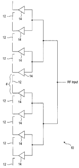
Referring now to the drawings, and initially to FIGS. 1 and 2, there are shown
two examples of a multiple antenna element antenna array 10, 10a in accordance
with the
~o invention. The antenna array 10, 10a of FIGS. 1 and 2 differ in the
configuration of the
feed structure utilized, FIG. 1 illustrating a parallel corporate feed
structure and FIG. 2
illustrating a series corporate feed structure. In other respects, the two
antenna arrays 10,
10a are substantially identical. Each of the arrays 10, 10a includes a
plurality of antenna
elements 12, which may comprise monopole, dipole or microstrip/patch antenna
is elements. Other types of antenna elements may be utilized to form the
arrays 10, 10a
without departing from the invention.
In accordance with one aspect of the invention, an amplifier element 14 is
operatively coupled to the feed of each antenna element 12 and is mounted in
close
proximity to the associated antenna element 12. In one embodiment, the
amplifier
zo elements 14 are mounted sufficiently close to each antenna element so that
no
appreciable losses will occur between the amplifier output and the input of
the antenna
element, as might be the case if the amplifiers were coupled to the antenna
elements by a
length of cable or the like. For example, the power amplifiers 14 may be
located at the
feed point of each antenna element. In one embodiment, the amplifier elements
14
zs comprise relatively low power, linear integrated circuit chip components,
such as
monolithic microwave integrated circuit (MMIC) chips. These chips may comprise
chips
made by the gallium arsenide (GaAs) heterojunction transistor manufacturing
process.
However, silicon process manufacturing or CMOS process manufacturing might
also be
utilized to form these chips.
3o Some examples of MMIC power amplifier chips are as follows:
C 30934v I 47176-00479
CA 02306650 2000-04-25
6
1. RF Microdevices PCS linear power amplifier RF 2125P, RF 2125, RF
2126 or RF 2146, RF Micro Devices, Inc., 7625 Thorndike Road, Greensboro, NC
27409, or 7341-D W. Friendly Ave., Greensboro, NC 27410;
2. Pacific Monolithics PM 2112 single supply RF IC power amplifier,
s Pacific Monolithics, In., 1308 Moffett Park Drive, Sunyvale, CA;
3. Siemens CGY191, CGY180 or CGY181, GaAs MMIC dual mode power
amplifier, Siemens AG, 1301 Avenue of the Americas, New York, NY;
4. Stanford Microdevices SMM-208, SMM-210 or SXT-124, Stanford
Microdevices, 522 Almanor Avenue, Sunnyvale, CA;
~ 0 5. Motorola MRFIC 1817 or MRFIC 1818, Motorola Inc., 505 Barton Springs
Road, Richardson, TX;
6. Hewlett Parckard HPMX-3003, Hewlett Packard Inc., 933 East Campbell
Road, Richardson, TX;
7. Anadigics AWT1922, Anadigics, 35 Technology Drie, Warren NJ 07059;
~s 8. SEI Ltd. P0501913H, l, Taya-cho, Sakae-ku, Yokohama, Japan; and
9. Celeritek CFK2062-P3, CCS 1930 or CFK2162-P3, Celeritek, 3236 Scott
Blvd., Sanata Clara, CA 95054.
In the antenna arrays of FIGS. 1 and 2, array phasing may be adjusted by
selecting
or specifying the element-to-element spacing (d) and/or varying the line
length in the
zo corporate feed. The array amplitude coefficient adjustment may be
accomplished
through the use of attenuators before or after the power amplifiers 14, as
shown in FIG.
3.
Referring now to FIG. 3, an antenna system in accordance with the invention
and
utilizing an antenna array of the type shown in either FIG. 1 or FIG. 2 is
designated
zs generally by the reference numeral 20. The antenna system 20 includes a
plurality of
antenna elements 12 and associated power amplifier chips 14 as described above
in
connection with FIGS. 1 and 2. Also operatively coupled in series circuit with
the power
amplifiers 14 are suitable attenuator circuits 22. The attenuator circuits 22
may be
interposed either before or after the power amplifier 14; however, FIG. 3
illustrates them
3o at the input to each power amplifier 14. A power sputter and phasing
network 24 feeds
C 30934v1 47176-00479
CA 02306650 2002-08-12
7
all of the power amplifiers I4 and their associated series connected
attenuator circuits 22.
An RF input 26 feeds into this power splatter and phasing network 24.
Referring to FICi. 4, an antenna system installation utilizing the antenna
system
20 of FIG3 is designated generally by tlne reference numertr) 40 FIG. 4
illustrates a
s base station or infrastructure configuration for a communications system
such as a
cellular system, a personal communic;atic.~ns system Pt'S or multi-channel
multipoint
distribution system (11-~S;I The <rntenna stn~cture or assembly 20 of FIG 3 is
mounted at the top of a tower or other support structure =12 A DC' bias tee 44
separates
signals received via coaxial cable 46 into I)(,' power and RF components, and
conversely
ro receives incoming RF signals from the antenna system 20 and delivers the
same to the
coaxial line or cable 46 which couples the: tower-rnountecl cc~rnponents to
ground based
components. The ground based components may include a DC power supply 48 and
an
RF input/output 50 from a transmitter/receiver (riot shown) which may be
located at a
remote equipment location, and hence is not shown in F~ICJ. 4. A similar DC
bias tee 52
rs receives the DC supply and RF input and couples them to the coa~aa) line
46, and
conversely delivers signals received from the antenna stnrctrrre 20 to the RF
input/output
50.
FIG. S illustrates a local multipoint distribution system (LMDS) employing the
antenna structure or system 20 as described above. In similar fashion to the
installation
zo of FIG 4, the installation of FIG 5 rrrounts the antenna system 20 atop a
tower/support
structure 42. Also, a coaxial cable 46, for example, arr I~F ccoaxial cable
for carrying RF
transmissions, runs between the tops of the tower/support stmc,~ture: and
ground based
equipment. 'the ground based equipment rnay include an RF transceiver 60 which
has an
RF input from a transmitter. Another similar RF transceiver 62 is located at
the top of
zs the tower and exchanges RF signals with the antenna structure or system 20.
A power
supply such as a DC supply 48 is also provided fear the antenna system 20, and
is located
at the top of the tower 4'Z in the embodiment shown in I~'IG ~.
FIG 6 illustrates a WLAN (wireless local area network installation) which also
mounts an antenna structure or system 20 of the type described above at the
top of a
3o tower/support structure 42. In simil<rr farshion to the installation of
FIG. 5, an RF
transceiver and power supply such as a DC'. supply 48 are also located at the
top of the
tower/support structure and are operatively coupled with the antenna system
20. A
second or remote RF transceiver f>0 rnay l:~e located adjacent the base of the
tower or
CA 02306650 2002-08-12
otherwise within range of a wireless link which links the transceivers 60 and
62, by use
of respective transceiver antenna elements 64 arrd 6(> as illrmtrated in FIG.
6.
FIGS. 7 and 8 illustrates examples c>f use of the antenna stnrctZrre or system
20 of
the invention in connection with irr-t~uilcling coa~municatian applications.
In FIG. 7,
s respective DC; bias tees 70 and 72 are linked by an RF coaxial cable 74 'fhe
DC bias tee
70 is located adjacent the antenna system 20 and has respective RF and DC'
lines
operatively coupled therewith fhe second C>C.' bias tee 72 is coupled to an RF
input/output from a transrnitter/receiver and to a suit~rble DC supply 48. The
DC bias
tees and DC supply operate in conjunction with the antenna syste:rn 20 and a
remote
ro transmitter/receiver (not shown) in much the same fashion as described
hereinabove with
reference to the system of FICi -=I.
In FIG. 8, the antenna system 20 receives an fZF line from a fiber-RF
transceiver
80 which is coupled through an optical fiber cable 82 to a second RF-fiber
transceiver 84
which may be located remotely fTOm thc: antenna and first transceiver 80. A DC
supply
rs or other power supply for the antenna may be located either remotely, as
illustrated in
FIG. 8 or adjacent the antenna system 2(J, if desired. The I)(: supply 48 is
provided with
a separate line operatively coupled to the antenn<~ system 20, in much the
same fashion
as illustrated, for example, in the installation of FIC~6.
What has been shown and described herein is a novel antenna array employing
2o power amplifier chips or modules at the fees of individual array antenna
elements, and
novel installations utilizing such an antenna system
Referring now to the remaining I~IGS 9-18, the various embodiments ofthe
invention shown have a number of' characteristics, three of which are
summarized below:
1) Use of two different (groups of) patch elements; one transmit, and one
zs receive. This results in substantial RF signal isolation (over 20 d:E3
isolation, at PCS
frequencies, by simply separating the patches horizontally by 4 inches)
without requiring
the use of a frequency diplexer at each antenna element (patch). 'This
technique can be
used on virtually any type of antenna element (dipole, rnonopole,
rnicrostrip/patch, etc.).
In some embodiments of a distrihuted antenna system, we use a collection of
3o elements (M vertical Tx elements 12, and M vertical Rx elements, 30), as
shown in FIGS.
9, l0 and I 1. FIGS. 9 and 10 show the elements in a series corporate feed
structure, for
both the Tx and Rx Note, that they can also be ire a parallel corporate feed
structure (not
shown); or the 'fx in a parallel corporate feed structure, and receive
elements in a series
feed structure (or vice-ver sa)
CA 02306650 2002-08-12
e)
2) Use of a "built in" Low Noise Amplificvr (L..NA) circuit or device; that
is,
built directly into the antenna, fc>r the receive (Rx) sick: I~ICi ~~ shows
the L.NA 140 after
the antenna elements 30 are summed via the series (or p~rrallel) cr,~rporate
feed stnrcture.
FICi. 10 shows the L:NA devices 140 (discrete de;vices) at the output of each
Rx element
s (patch), before being RI~ summed.
The LNA device 140 at the Rx antenna red~rces the overall system noise figure
(NF), and increases the sensitivity of the system, to tyre signal emitted by
the remote
radio. This therefore, helps to increase the range of the receive link
(uplink).
The similar use of power amplifier (PA) devic,e;s 14 (chips) at the transmit
(Tx)
ro elements has been discussed above
3) Use of a low power frequency diplexer 150 (shown in FIGS 9 and 10).
In conventional tower top systems (such as "Cell Boosters"), since the power
delivered
to the antenna (at the input) is high power RF, a high power ffequency
diplexer must be
used (within the Cell Booster, at the tower top) In onr ,system, since the RI~
power
rs delivered to the {Tx) antenna is low (typically less than 10C)
rnilliwatts), a low power
diplexer 150 can be used
Additionally, in corwentional system, the diplexer isolation is typically
required
to be well over 60 dB; often up to 80 or 90 dB isolation between the uplink
and downlink
signals.
zo Since the power output from our system, at each patch, is )ow power (less
than 1
-2 Watts typical), and since we have alre~rdy achieved (;spatial) isolation
via separating
the patches, the isolation requirements of~our diplexer is nnrch less.
In each of the embodiments illustrated herein, a final transmit rejection
filter (not
shown) would be used in the receive path. This filter might be built into the
or each
zs LNA if desired; or might be coupled in circuit ahead of' the or each LNA.
Referring now to FICi. I l, this embodiment uses two separate antenna elements
(arrays), one for transmit 12, and one for receive 30, e.g , a plurality of
transmit (array)
elements 12, and a plurality of receive (array) elements ~30 The elements can
be dipoles,
monopoles, microstrip (patch) elements, or any other r~rdiating antenna
element. The
3o transmit element (array) will use a separate corporate feed (not shown)
from the receive
element array. Each array (transmit 30 and receive 12) is shown in a separate
vertical
column; to shape narrow elevation beams. This can also be done in the same
manner for
two horizontal rows of arrays (not shown); shaping narrow azimuth beams
CA 02306650 2000-04-25
Separation (spatial) of the elements in this fashion increases the isolation
between
the transmit and receive antenna bands. This acts similarly to the use of a
frequency
diplexer coupled to a single transmit/receive element. Separation by over half
a
wavelength typically assures isolation greater than 10 dB.
The backplane/reflector 155 can be a flat ground plane, a piecewise or
segmented
linear folded ground plane, or a curved reflector panel (for dipoles). In
either case, one
or more conductive strips 160 (parasitic) such as a piece of metal can be
placed on the
backplane to assure that the transmit and receive element radiation patterns
are
symmetrical with each other, in the azimuth plane; or in the plane orthogonal
to the
~o arrays. FIG. 11 illustrates an embodiment where a single center strip 160
is used for this
purpose and is described below. However, multiple strips could also be
utilized, for
example over more strips to either side of the respective Tx and Rx antenna
element(s).
This can also be done for antenna elements (Tx, Rx) oriented in a horizontal
array (not
shown); i.e., assuring symmetry in the elevation plane. For antenna elements
(Tx, Rx)
is which are non-centered on the ground plane 155, as shown in FIG. 11, the
resulting
radiation patterns are typically non-symmetric; that is, the beams tend to
skew away from
the azimuth center point. The center strip 160 (metal) "pulls" the radiation
pattern beam,
for each array, back towards the center. This strip 160 can be a solid metal
(aluminum,
copper, . . .) bar; in the case of dipole antenna elements, or a simple copper
strip in the
zo case of microstrip/patch antenna elements. In either case, the center strip
160 can be
connected to ground or floating; i.e., not connected to ground. Additionally,
the center
strip 160 (or bar) further increases the isolation between the transmit and
receive antenna
arrays/elements.
The respective Tx and Rx antenna elements can be orthogonally polarized
Zs relative to each other to achieve even further isolation. This can be done
by having the
receive elements 30 in a horizontal polarization, and the transmit elements 12
in a
vertical polarization, or vice-versa. Similarly, this can be accomplished by
operating the
receive elements 30 in slant-45 degree (right) polarization, and the transmit
elements 12
in slant-45 degree (left) polarization, or vice-versa.
3o Vertical separation of the elements 12 in the transmit array is chosen to
achieve
the desired beam pattern, and in consideration of the amount of mutual
coupling that ca~
C 30934v1 47176-00479
CA 02306650 2000-04-25
11
be tolerated between the elements 12 (in the transmit array). The receive
elements 30 are
vertically spaced by similar considerations. The receive elements 30 can be
vertically
spaced differently from the transmit elements 12; however, the corporate
feeds) must be
compensated to assure a similar receive beam pattern to the transmit beam
pattern, across
s the desired frequency band(s). The phasing of the receive corporate feed
usually will be
slightly compensated to assure a similar pattern to the transmit array.
Most existing Cellular/PCS antennas use the same antenna element or array for
both transmit and receive. The typical arrangement has a RF cable going to the
antenna,
which uses a parallel corporate feed structure; thus all the feed paths, and
the elements,
io handle both the transmit and receive signals. Thus, for these types of
systems, there isn't
a need to separate the elements into separate transmit and receive
functionalities. The
characteristics of this approach are:
a) A single ( 1 ) antenna element (or array) used; for both Tx and Rx
operation.
is b) No constriction or restriction on geometrical configuration.
c) One ( 1 ) single corporate feed structure, for both Tx and Rx operation.
d) Element is polarized in the same plane for both Tx and Rx.
For (c) and (d), there are some cases (i.e. dual polarized antennas) that use
cross-
polarized antennas (literally two antenna structures, or sub-elements, within
the same
zo element), with the Tx functionality with its own sub-element and corporate
feed
structure, and the Rx functionality with its own sub-element and separate
corporate feed
structure.
In FIG 11, we split up the transmit and receive functionalities into separate
transmit and receive antenna elements, so as to allow separation of the
distinct bands
zs (transmit and receive). This provides added isolation between the bands,
which in the
case of the receive path, helps to attenuate (reduce the power level of the
signals in the
transmit band), prior to amplification. Similarly, for the transmit paths, we
only (power)
amplify the transmit signals using the active components (power amplifiers)
prior to
feeding the amplified signal to the transmit antenna elements.
3o As mentioned above, the center strip aids in correcting the beams from
steering
outwards. In a single column array, where the same elements are used for
transmit and
C 30934v1 47176-00479
CA 02306650 2000-04-25
12
receive, the array would likely be placed in the center of the antenna (ground
plane) (see
e.g., FIG. 12, described below). Thus the azimuth beam would be centered
(symmetric)
orthogonal to the ground plane. However, by using adjacent vertical arrays
(one for Tx
and one for Rx), the beams become asymmetric and steer outwards by a few
degrees.
s Placement of a parasitic center strip between the two arrays "pulls" each
beam back
towards the center. Of course, this can be modeled to determine the correct
strip width
and placements) and locations of the vertical arrays, to accurately center
each beam.
The characteristics of this approach are:
a) Two (2) different antenna elements (or arrays) used; one for Tx and one
~o for Rx.
b) Geometrical configuration is spaced apart adjacent placement of Tx and
Rx elements (as shown in FIG. 11 ).
c) Two (2) separate corporate feed structures used, one for Tx and one for
Rx.
~s d) Each element can be polarized in the same plane, or an arrangement can
be constructed where the Tx element(s) are in a given polarization, and the Rx
elements
are all in an orthogonal polarization.
The embodiment of FIG. 12 uses two separate antenna elements, one for transmit
12, and one for receive 30, or a plurality of transmit (array) elements, and a
plurality of
Zo receive (array) elements. The elements can be dipoles, monopoles,
microstrip (patch)
elements, or any other radiating antenna element. The transmit element array
will use a
separate corporate feed from the receive element array. However, all elements
are in a
single vertical column; for beam shaping in the elevation plane. This
arrangement can
also be used in a single horizontal row (not shown), for beam shaping in the
azimuth
zs array. This method assures highly symmetric (centered) beams, in the
azimuth plane, for
a column (of elements); and in the elevation plane, for a row (of elements).
The individual Tx and Rx antenna elements in FIG. 12, can be orthogonally
polarized to each other to achieve even further isolation. This can be done by
having the
receive patches 30 (or elements, in the receive array) in the horizontal
polarization, and
3o the transmit patches 12 (or elements) in the vertical polarization, or vice-
versa.
Similarly, this can be accomplished by operating the receive elements in slant-
45 degree
C 30934v1 47176-00479
CA 02306650 2000-04-25
13
(right) polarization, and the transmit elements in slant-45 degree (left)
polarization, or
vice-versa.
This technique allows placing the all elements down a single center line. This
results in symmetric (centered) azimuth beams, and reduces the required width
of the
s antenna. However, it also increases the mutual coupling between antenna
elements,
since they should be packed close together, so as to not create ambiguous
elevation lobes.
The characteristics of this approach are:
a) Two (2) different antenna elements (or arrays) used; one for Tx and one
for Rx.
io b) Geometrical configuration is adjacent, collinear placement.
c) Two (2) separate corporate feed structures used, one for Tx and one for
Rx.
d) Each element is polarized in the same plane, or the Tx element(s) are all
in a given polarization, and the Rx elements are all in an orthogonal
polarization.
is The embodiment of FIG. 13 uses a single antenna element (or array), for
both the
transmit and receive functions. In this case, a patch (microstrip) antenna
element is used.
The patch element 170 is created via the use of a multi-element (4-layer)
printed circuit
board, with dielectric layers 183, 185, 187 (see FIG. 14). The antennas can be
fed with
either a coaxial probe (not shown), or aperture coupled probes or
microstriplines 180,
Zo 182. For the receive function, the feed microstripline l 82 is oriented
orthogonal to the
feed stripline (probe) 180 for the transmit function.
The elements can be cascaded, in an array, as shown in FIG. 13, for beam
shaping
purposes. The RF input 190 is directed towards the radiation elements via a
separate
corporate feed from the RF output 192 (on the receive corporate feed), ending
at point
zs "A". Note that either or both corporate feeds 180, 182 can be parallel or
series corporate
feed structures.
The diagram of FIG. 13 shows that the receive path RF is summed in a series
corporate feed, ending at point "A" ( 192) preceded by a low noise amplifier
(LNA).
However, low noise amplifiers, (LNAs), can be used directly at the output of
each of the
3o receive feeds (not shown in FIG. 13), prior to summing, similar to the
showing in FIG. 4,
as discussed above.
C 30934v1 47176-00479
CA 02306650 2000-04-25
14
The transmit and receive RF isolation is achieved via orthogonal polarization
taps
from the same antenna (patch) element, as shown and described above with
reference to
FIGS. 13 and 14. FIG. 14 indicates, in cross-section, the general layered
configuration of
each element 170 of FIG. 13. The respective feeds 180, 182 are separated by a
dielectric
s layer 183. Another dielectric layer 185 separates the feed 182 from a ground
plane 186,
while yet a further dielectric layer separates the ground plane 186 from a
radiating
element or "patch" 188.
This concept uses the same antenna physical location for both functionalities
(Tx
and Rx). A single patch element (or cross polarized dipole) can be used as the
antenna
io element, with two distinct feeds (one for Tx, and the other for Rx at
orthogonal
polarization). The two antenna elements (Tx and Rx) are orthogonally
polarized, since
they occupy the same physical space.
The characteristics of this approach are:
a) One ( 1 ) single antenna element (or array), used for both Tx and Rx.
~s b) No construct on geometrical configuration.
c) Two (2) separate corporate feed structures used, one for Tx and one for
Rx.
d) Each element contains two (2) sub-elements, cross polarized (orthogonal)
to one another.
zo The embodiments of FIGS. 15-16 show two (2) ways to direct the input and
output RF from the Tx/Rx active antenna, to the base station.
FIG. 15 shows the output RF energy, at point 192 (of FIG. 8), and the input RF
energy, going to point 190 (of FIG. 13), as two distinctly different cables
194, 196.
These cables can be coaxial cables, or fiber optic cables (with RF/analog to
fiber
zs converters, at points "A" and "B"). This arrangement does not require a
frequency
diplexer at the antenna (tower top) system. Additionally, it does not require
a frequency
diplexer (used to separate the transmit band and receive band RF energies) at
the base
station.
FIG. 16 shows the case where the output RF energy (from the receive array) and
3o the input RF energy (going to the transmit array), are diplexed together
(via a frequency
diplexer 100), within the antenna system so that a single cable 198 runs down
the tower
C 30934v1 47176-00479
CA 02306650 2000-04-25
1$
(not shown) to the base station 104. Thus, the output/input to the base
station 104 is via
a single coaxial cable (or fiber optic cable, with RF/analog to fiber optic
converter). This
system requires another frequency diplexer 102 at the base station 104.
FIGS. 17 and 18 show another arrangement which may be used as a
s transmit/receive active antenna system. The array comprises of a plurality
of antenna
elements 110 (dipoles, monopoles, microstrip patches, ...) with a frequency
diplexer 112
attached directly to the antenna element feed of each element.
In FIG. 17, the RF input energy (transmit mode) is split and directed to each
element, via a series corporate feed structure 115 (this can be microstrip,
stripline, or
~o coaxial cable), but can also be a parallel corporate feed structure (not
shown). Prior to
each diplexer 112, is a power amplifier (PA) chip or module 114. The RF output
(receive mode) is summed in a separate corporate feed structure 116, which is
amplified
by a single LNA 120, prior to point "A," the RF output 122.
In FIG. 18, there is an LNA 120 at the output of each diplexer 112, for each
~s antenna (array) element 110. Each of these are then summed in the corporate
feed 12$
(series or parallel), and directed to point "A," the RF output 122.
The arrangements of FIGS. 17 and 18 can employ either of the two connections
(described in FIGS. 1$ and 16), for connection to the base station 104
(transceiver
equipment).
2o What has been shown and described herein is a novel antenna array employing
power amplifier chips or modules at the feed of individual array antenna
elements, and
novel installations utilizing such an antenna system.
While particular embodiments and applications of the present invention have
been illustrated and described, it is to be understood that the invention is
not limited to
is the precise construction and compositions disclosed herein and that various
modifications, changes, and variations may be apparent from the foregoing
descriptions,
and are to be understood as forming a part of the invention insofar as they
fall within the
spirit and scope of the invention as defined in the appended claims.
C 30934v1 47176-00479