Note: Descriptions are shown in the official language in which they were submitted.
CA 02306842 2000-04-18
WO 99/237b0 PCT/US98/Z3282
RECEIVER FOR A RECONFIGURABLE RADIO SYSTEM AND METHOD THEREFOR
BACKGROUND OF THE INVENTION
This application claims the benefit of the U.S. Provisional
Applications Serial Number 60/064,097 filed November 3, 1997;
Serial Number 60/064,132 filed November 3, 1997; and Serial
Number 60/064098 filed November 3, 1997.
This application relates to a field programmable radio
frequency communications systems in general, and more
particularly to a system and method for trellis coded modulation
( "TCM" ) .
Descriptions of the various components of the system are
contained in co-pending patent applications owned by the assignee
hereof and filed concurrently herewith, specifically: U.S.
Patent Application S. N.
entitled
"Reconfigurable Radio System Architecture And Method Therefor";
U.S. Patent Application S.N. ,
entitled "A Control System For Controlling the Processing Data of
a First In First Out Memory and Method Therefor"; U.S. Patent
Application S.N. , entitled "Configurable
Circuits for Field Programmable Radio Frequency Communications
Equipment and Methods Therefor"; U.S. Patent Application S.N. -
entitled "A System For Accelerating
the Reconfiguration of a Transceiver and Method Therefor"; U.S.
Patent Application S.N.
entitled "A
Field Programmable Radio Frequency Communications Equipment
Including A Configurable IF Circuit, And Method Therefore" ;
U.S. Patent Application S.N.
entitled
CA 02306842 2000-04-18
WO 99/23760 PCT/US98rZ3282
"A Field Programmable Modulator-Demodulator Arrangement For Radio
Frequency Communications Equipment, And Method Therefor"; U.S.
Patent Application S.N. , entitled "A Digital
Noise Blanker For Communications Systems and Methods Therefor";
U.S. Patent Application S.N.
entitled
"TCM Revisiting System and Method"; U.S. Patent Application S.N.
entitled "Least Squares Phase Fit As
Frequency Estimate"; U.S. Patent Application S.N.
entitled "Polar Computation of Branch Metrics For TCM";
U.S. Patent Application S.N.
entitled
"Efficient Modified Viterbi Decoder"; each of which is
incorporated herein by reference.
In digital phase modulation, the transmission of data is
accomplished by shifting of the carrier phase to a specific value
for each symbol transmitted; such modulation usually referred to
as phase shift keying ("PSK"). In a PSK system, phase shift
points can be considered as being located about a 360 degree
constellation of points representing a sine wave. The number of
data points (branches) used in a PSK system will depend upon the
complexity of data to be transmitted. For example, the PSK
system can take the form of a binary PSK with the constellation
divided into two data points, a QPSK with the constellation
divided into four data points, an BPSK with the constellation
phase divided into eight branches, a 16PSK with the constellation
divided into 16 branches. The 16 PSK system will include 16 data
points about the constellation designated as 0000, 0001, 0010,
2
CA 02306842 2000-04-18
WO 99/Z3760 PCTNS98/23282
0011, etc. As the number of data points (branches) increase, the
complexity of the communications system increases.;
In these types of systems, the data often involves Trellis
Coded Modulation (TCM). A receiver system for receiving the
trellis modulated signals often includes a Viterbi algorithm to
decode the information. In a given PSK system only a finite
number of sets can be transmitted. The Viterbi algorithm
functions to help make a determination of the probability that
the symbol set received was the symbol set transmitted.
In a Trellis Coded Modulation where each symbol is to
transmit k bits, some number m of the least significant bits are
sent to an encoder which outputs m + p bits to map into the
waveform which has p possible symbols where p=2 ** k+p. The k=m
bits are not encoded. The number of possible states that the
encoder may have is dependent on the contraint length of the
code. In a trellis representation of the waveform, the uncoded
bits are represented as parallel paths in the transitions between
trellis states.
For optimum demodulation of TCM, the parallel paths are
followed through the trellis. This dramatically complicates the
decoding of Trellis Codes compared to normal convolutional codes
because branch metrics have to be computed for all the parallel
paths, and the best parallel path needs to be stored for all
surviving paths.
3
CA 02306842 2000-04-18
WO 99/23760 PCT/US98/23282
The standard way of reducing the complexity is to make a
decision on the MSBs immediately and then decode the LSB in light
of that decision. This eliminates the parallel paths and
therefore reduces the complexity of the decoding algorithm.
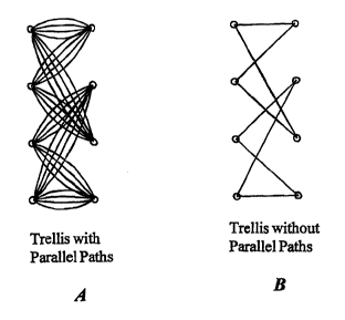
Figures 1a and 1b show a trellis with parallel paths and a
trellis without parallel paths respectively.
While reducing the complexity of the decoding algorithm,
making an immediate decision on the MSBs also increases the
likelihood of an error for the MSBs because the effect of the
LSBs is to shift the waveform nearer to the decision boundaries
of the MSBs. This makes the MSB decision more susceptible to
noise. Figure 2 illustrates this concept for an 8 PSK system.
It can be seen that the distance of the signal from the MSB
decision boundary depends on the values of the LSBs. These LSBs
then act as an interferer when deciding the MSBs.
Accordingly, it is an object of the present invention to
provide a novel method and system for reducing the likelihood of
errors induced by the LSBs in TCM.
It is another object of the present invention to provide a
novel system and method for eliminating the parallel paths of a
trellis in TCM.
Further, the computation of the trellis branch metrics using
textbook approaches are very intensive and require a great deal
of microprocessor cycles.
4
CA 02306842 2000-04-18
WO 99123760 PCT/US98/23282
Therefore, it is yet another object of the present invention
to provide a novel method and system for processing samples by
exploiting the inherent qualities of the form by which they are
represented.
In TCM, the decoding of the received signal may be
accomplished through the use of Viterbi decoders. Prior art (?)
Viterbi decoders exist which improve performance of a
convolutional decoder by 1.5 dB. However, such decoders greatly
increase the complexity of the algorithm.
It is yet a further object of the present invention to
provide a novel method and system to reduce the complexity of the
processing associated with Viterbi decoders without reducing the
performance of the algorithm.
Finally, when receiving a signal, a frequency estimate must
be made on a pure carrier. The effectiveness of the carrier
estimate will dictate the required length of the preamble of a
data waveform. The shorter the preamble the better for
applications such as networking. Processing should be as simple
as possible so that the estimate can be done and corrections made
before the data starts.
It is still a further object of the present invention to
provide a novel method and system for providing frequency
estimation of a carrier.
It is further an object of this invention to provide a novel
and improved radio frequency receiver that includes a simplified
arrangement for providing an estimate of the carrier signal of
CA 02306842 2000-04-18
WO 99/23760 PCT/US98/23282
the received signal and correlate the demodulator to the estimate
of the carrier signal.
It is also an object of this invention to provide a novel
and improved receiver for receiving and decoding TCM signals.
It is also and object of this invention to provide a novel
and improved radio frequency receiver for reducing the likelihood
of errors in decoding received TCM signals.
It is also an object of this invention to provide a novel
and improved radio frequency receiver for simplified decoding of
received TCM signals without significant degradation of
performance.
It is also an object of this invention to provide a novel
and improved radio frequency receiver for decoding TCM signals
involving a decoder arrangement including simplified polar
computations and Viterbi decoding.
These and many other objects and advantages of the present
invention will be readily apparent to one skilled in the art to
which the invention pertains from a perusal of the claims, the
appended drawings, and the following detailed description of the
preferred embodiments.
6
CA 02306842 2000-04-18
WO 99/23760 PCT/US98/23282
BRIEF DESCRIPTION OF THE DRAWINGS
Figure la illustrates a trellis having parallel paths.
Figure lb illustrates a trellis without parallel paths.
Figure 2 illustrates the MSB decision boundary for a 8 PSK
prior art system.
Figure 3 is a block diagram of a field programmable radio
frequency communications system, including a configurable digital
IF subsystem, that can be field configured to operate in the
receiver or transmitter mode of operation, the selected signaling
scheme or waveform, and tailor the circuits with corresponding
parameters for signal processing including polar conversion,
trellis modulation decoding, and frequency estimation and control
in the receiver mode of operation.
Figure 4 is an expanded block diagram of the field
configurable radio frequency communications system of Figure 3
illustrating the interconnection of various subsystems.
Figures 5A and 5B include a flow diagram explaining the
steps involved in configuring the field programmable radio
frequency communications system.
Figures 6A and 6B include an expanded block diagram of the
field configurable radio frequency communications system showing
interconnections between various subsystems when configured in
the transmit mode.
7
CA 02306842 2000-04-18
WO 99/23760 PCTNS98lZ3282
Figure 7 is a block diagram of the radio frequency sub-
system portion of the field configurable radio frequency
communications system.
Figure 8 is a block diagram of the intermediate frequency
(IF) sub-system portion of the field programmable radio frequency
communications system including a demodulation and signal
processing system, a modulation and signal processing system, a
baseband signal processing system, and bus structure, that can be
configured to provide the Cartesian to polar digital signal
conversion.
Figure 9 is a block diagram of the field configurable
digital IF demodulator and signal processing circuit of the of
the IF sub-system the for use in the receive mode of operation
including an input for frequency control.
Figure 10 is a block diagram of the field configurable radio
frequency communication system of Figure 3 and Figure 4
configured in the PSK receiver mode of operation and configured
to include the polar computation of branch metrics, modified
viterbi and TCM revisited algorithms.
Figure 11 is a diagram illustrating the MSB decision
boundary for one embodiment of the present invention.
Figure 12 a block diagram illustrating the revisiting
algorithm implemented for one embodiment of the present
invention.
8
CA 02306842 2000-04-18
WO 99/Z37b0 PCT/US98/23282
Figure 13 is a block diagram of the full configurable radio
frequency communications system of Figure 3 and Figure 4
configured in the receiver mode of operation including the least
square fit algorithm.
Figure 14 illustrates a preamble used in estimating the
frequency for receiving a signal.
DESCRIPTION OF PREFERRED EMBODIMENTS
The present invention finds applicability in programmable
digital processor type of radio frequency communications system.
Table of Contents
I. Field Programmable Radio Communications System Description
(Figures 3-8)
II. Receiver Demodulator (Figures 8-10)
A. TCM Revisiting Algorithm (Figures 10-12)
B. Polar Computation of Branch Metrics (Figure 10)
C. Modified Viterbi Algorithm (Figure 10)
D. Least Squares Phase Fit As Frequency Estimate
(Figures 13-14)
I. FIELD PROGRAMMABLE RADIO COMMUNICATIONS SYSTEM DESCRIPTION
9
CA 02306842 2000-04-18
WO 99/23760 PCT/US98/Z3282
Figure 3 describes a field programmable radio frequency
communications system that can be programmed by a user to form a
digital signal processing system 10 that is adapted to be coupled
to a radio frequency receiver and or transmitter subsystem 12 to
configure a radio frequency receiver and/or transmitter system to
operate with any of a plurality of radio frequency waveforms or
signaling schemes, such as, AM, AME, A3E, H3E, J3E, CW, SSB, M-
PSK, QAM, ASK, and angular modulation, such as, FM, PM, FSK, CMP,
MSK, CPFSK etc. The multi bit digital instructions, commands, and
software to configure the digital processing system 10 can be
provided from a remote location or stored in a configuration non-
volatile memory 14. When using the memory 14, instructions are
down loaded into the memory 14 from the configuration input
circuit 16 under the control of the configuration control system
18. In response to instructions provided from the user input
circuit 26, the configuration control system 18 (in response to
instructions or commands stored in the configuration memory 14)
connects selected ones of a plurality of configurable digital
signal processors (CDSP) 20 and 22, downloads the software
program, and configures the digital IF subsystem 24 in a receiver
or transmitter mode of operation with the radio frequency
subsystem 12 to function in accordance with the signaling scheme
selected by the user. Hence, the arrangement is such that a
single piece of equipment can be, in response to instructions
from the user, configured to operate with a radio frequency
subsystem 12 as a substantially universal type of radio frequency
CA 02306842 2000-04-18
WO 99/23760 PCTNS98/23Z82
communications system, controlled the configurations and software
programs inputted directly or loaded into the configuration
memory 14.
As illustrated in Figure 4, the configuration control system
.18 includes a re-programmable processor subsystem A (which, for
example, can be the central control digital signal processor
[BIOP] 28), coupled to the radio configuration download port 16,
the re-programmable keyboard display unit (KDU) or computer (CPU)
26, the architecture configuration storage device (which, for
example, can be a large memory 14), and a re-configurable
hardware element A (which, for example can be the central control
field programmable field array [CFPGA] 30). The central control
CFPGA 30 is also coupled to a re-programmable processor subsystem
E (which, for example can be the control digital signal processor
[CDSP] 32), the intermediate frequency (IF) subsystem which is
configurable as a digital IF modulator or demodulator and
configurable baseband signal processing system (which, for
example, can be in the form of an application specific integrated
circuit [ASIC] 24), the configurable digital signal processor 20
and the configurable digital signal processor 22. The IF
subsystem 24 is coupled to the radio frequency subsystem 12 and
is configurable to provide modulated IF signals to a transmitter,
or to receive RF signals to be demodulated.
The configurable digital signal processing circuit 20
includes a re-programmable processor subsystem B (which, for
11
CA 02306842 2000-04-18
WO 99/23760 PCTNS98/23282
example can be the auxiliary digital signal processor [ADSP] 34)
that is coupled through a re-configurable hardware element B
(which, for example can be the auxiliary FPGA [AFPGA] 36) to the
CFPGA 30. The configurable digital signal processing circuit 22
includes a re-programmable processor subsystem C (which for
example can be the voice/data DSP [VDSP] 38) that is coupled
through a re-configurable hardware element C (which for example
can be the voice/data FPGA [VFPGA] 40) to the CFPGA 30. The
configurable digital signal processing circuit 22 also includes a
re-programmable processor subsystem D (which, for example can be
the security processor system [SDSP] 42) that is coupled through
a re-configurable hardware element D (which, for example, can be
the security FPGA [SFPGA] 44) to the CFPGA 30. Although the
hardware elements A, B, C, and D are identified as field
programmable gate arrays (FPGA), the hardware elements can also
include a variety of signal processing circuits. Although the
digital signal processing system 10 includes a specific
combination of interconnected re-programmable processor
subsystems, re-configurable hardware element, architecture
configuration storage device, and intermediate frequency
subsystem, such elements and equivalents thereof could be used in
various other arrangements and still include the inventive
concepts of the digital signal processing system.
The BIOP 28 is the main control system which controls the loading
of the configuration multi bit commands, operating parameters and
12
CA 02306842 2000-04-18
WO 99/23760 PCT/US98/23282
configuration software from memory 14 (or directly from a remote
input) into the various subsystems of the digital signal
processing system. It also functions as the interface to the
user KDU 26 and down load port 16. The CFPGA 30 is the main
interconnect unit involved in configuration of the digital signal
processing system for receiver or transmitter modes of operation
and to tailor the system 10 for the particular signaling scheme
or waveform selected. As the central control element, the CFPGA
can be configured to provide two levels of control, ie the
software level and the circuit (hardware) function processes,
command signal flow, and interconnect. The CFPGA 30 can also
include a variety of digital signal processing circuits, such as,
for example, active signal processing circuit, (such as, a
veterbi decoder, RF AGC, peak sample registers, transmit gain,
thermal cut back, etc.) as well as providing inter processor
communications ( such as, reading signals in and out of the IF
ASIC 24, and assigning control values to various subsystems). In
the present invention, the CFPGA 30 can also be downloaded to
include the Efficient Modified Viterbi Algorithm 306 of Figure
10.
All other FPGAs in the system can also be configured to
include multi bit signal processing circuits. For example, the
AFPGA 36 can alternately be downloaded to include the Efficient
Modified Viterbi Algorithm 306 of Figure 10. The CDSP 32, which
functions with the BIOP 28 to operate the system once configured,
13
CA 02306842 2000-04-18
wo ~n3~6o Pcr~s9sn3zsz
can also be downloaded to include the Polar Computation of Branch
Metrics 300, the Polar Sample Storage 302, the Revisiting
Algorithm 304 functions of Figure 10, and the Least Square Fit
308 function of Figure 13. The VDSP 38 can, for example be
configured to process multi bit digital voice and data samples,
or signals for the selected signaling scheme or waveform. The
VDSP 38 can be programmed to include specific signal processing
functions, such as, voice or data compression. The SDSP 42 can
be programmed and connected in the system 10 to provide a special
functions, such as, for example voice and data encryption. In
the present invention, the CDSP 32 can alternately be downloaded
to include the Polar Computation of Branch Metrics 300, the Polar
Sample Storage 302, the Revisiting Algorithm 304 functions of
Figure 10, and the Least Square Fit 308 function of Figure 13.
The IF ASIC 24 can be programmed to be configured to provide the
demodulation function for multi bit digital signals in the
receive mode, the modulation function in the transmit mode, and
to provide multi bit digital signal baseband signal processing.
The various radio configurations are down laaded into the memory
14 from the download port 16 (or directly inputted from a remote
source) under the control of the BIOP 28. In the present
invention, the IF ASIC 24 will be configured in the receive mode
of operation to provide a polar output to the Polar Computation
of Branch Metrics 300 arrangement of Figure 10 and to receive a
frequency offset signal from the Least Square Fit 308 arrangement
of Figure 13 by the frequency offset registers of the wideband
14
CA 02306842 2000-04-18
WO 99/23760 PCT/US98/23282
NCO 164 of Figure 9 or the narrow band NCO 200 of Figure 8. If
configurations are loaded into the memory 14, all the user needs
to do is to select the receiver or transmitter mode of operation,
the signaling scheme or waveform, along with other communications
system parameters, push the enter button, and the digital signal
processing system 10 will automatically configure to the desired
RF communications system for the user selected mode of operation.
If the configuration is directly inputted, the~system selection
instruction are directly inputted.
The flow diagram of Figure 5 describes the various steps
involved in configuring the radio frequency communications
system. In step 48, the radio operator enters a change of mode
of operation in the KDU 26. The BIOP 28 processes the KDU 26
information and displays text on the KDU screen (step 50) and
determines if the mode requires FPGA changes and/or processor
software changes (step 52). If not , the radio communications
system keeps operating unchanged (step 54). If changes are
needed, the BIOP 28 puts the radio communications system in the
idle mode (step 56). A determination is made if the CFPGA 30 is
to be changed (step 58). If so, the BIOP 28 loads the new multi
bit commands or code from the memory 14 into the CFPGA 30 (step
60). For example, at this time the Efficient modified Viterbi
Algorithm software program of Figure 10 can be downloaded into
the CFPGA 30. A check is made if the load is complete (steps 62,
63 and 64).
CA 02306842 2000-04-18
WO 99/23760 PCT/US98/23282
If the step 58 determines that a CFPGA 30 changes is not
required, or the new multi bit code is successfully loaded (step
62), then a determination is made if the CDSP 32 software
requires change (step 66). If so, the BIOP 28 loads the new
software in the CDSP 32 (step 68) and a check is made if the load
is complete (steps 70, 72 and 74). If the step 66 determines
that a CDSP 32 change is not required, or the new code is
successfully loaded (step 70), then a determination is made if
the AFPGA 36 requires change (step 76). If so, then the BIOP 28
loads the new code in the AFPGA 36 (step 78) and a check is made
to verify that the load is complete (steps 80, 82 and 84). For
example, at this time the Polar Computation of Branch Metrics,
Polar Sample Storage, and the Revisiting Algorithm software
programs of Figure 10 and the Least Square Fit software program
of Figure 13 can be downloaded into the CDSP 32.
If the step 76 determines that a AFPGA 36 change is not
required, or the new code is successfully loaded (step 80), then
a determination is made if the ADSP 34 requires a software
change (step 86, Figure 5B). If so, then the BIOP 28 loads the
new software in the ADSP 34 (step 88) and a check is made if the
load is complete (steps 90, 92 and 94). For example, at this
time the Polar Computation of Branch Metrics, Polar Sample
Storage, and the Revisiting Algorithm software programs of Figure
and the Least Square Fit software program of Figure 13 can be
downloaded into the ADSP 34. If the load of step 90 is complete,
16
CA 02306842 2000-04-18
WO 99/23760 PCTNS98/23282
or no change is required, then in step 96 the BIOP 28 sends
commands to the VDSP 38 and SDSP 42 to configure the DSPs for the
new mode and a check is made to verify that the load is complete
(steps 90, 92 and 94). For example, at this time the Efficient
modified Viterbi Algorithm software program of Figure 10 can be
downloaded into the AFPGA 36.
At this time the process separates into three branches. In
branch B the step 98 determines if the VFPGA 40 requires a
change. If not, step 100 initializes the VDSP 38 and step 102
notifies the BIOP 28 that the VDSP is ready. If the VFPGA 40
needs a change, the step 104 has the VDSP 38 load new code into
the VFPGA 40. The steps 106, 108, and 110 monitor to determine
if the new code load in the VFPGA 40 is complete and allows the
step 100 to initialize the VDSP 38. In branch C, step 112
initializes the SDPS 42 and the step 114 tells the BIOP 28 that
the SDSP 42 is ready.
In the main branch of the process, in step 116 the BIOP 28
checks the status of the VDSP 38 and the SDSP 42. If the step
118 determines that the VDSP and/or the SDSP are not ready, the
step 120 delays the process until the VDSP and the SDSP are
ready. Thereafter, the BIOP 28 initializes the system. Once the
system initialization is complete, in the step 122 the CDSP 32
initializes the IF ASIC 24. For example, the Cartesian to polar
converter 206 of Figure 8 can be configured to provide received
signals in digital form for the Polar Computation of Branch
17
CA 02306842 2000-04-18
WO 99/23760 PCT/US98/Z3282
Metrics of Figure 10, and the IF ASIC can be configured in the
received mode of operation with the output of the Least Square
Fit output of Figure 13 of line DR3 applied to the frequency
offset input of the wideband NCO 164 receiver demodulator
configuration of Figure. 9 or the narrowband NCO 200 of Figure 8.
Thereafter, the step 124 indicates the radio frequency
communications system is now in operation in the new user
selected mode.
Figures 6A and 6B illustrate the interconnection of the
various subsystems of the digital RF communications system
interconnected to operate in a coded transmit mode. All the
subsystems are interconnected by a data 111, address 113 and
control 115 bus. In addition, some subsystems are interconnected
by a serial data bus 117. The DSP type subsystems 28, 32, 34, 38
and 42 include signal and control processing arrangements
including RAM memory 121 and a digital signal processor DSP 123
or microprocessor 119. In addition the DSP type subsystems 28,
32, 34 and 38 include input/output devices 109. The SDSP 42
includes encryption devices 101. The VFPGA 40 is configured to
include a FIFO 105 register, while the SFPGA 44 is configured to
include a UART 107. The multi bit signals to be transmitted are
inputted into the VDSP 38, encrypted by the SDSP 42, and coupled
through the SFPGA 44, the VFPGA 40, the CFPGA 30, the CDSP 32,
the IF ASIC 24 and the radio frequency subsystem 12 in the
transmit mode of transmission via the antenna 11.
18
CA 02306842 2000-04-18
WO 99123760 PCT/US98/23282
Figure 7 illustrates the receiver section 125 and the
transmitter section 126 of the radio frequency subsystem 12. The
receiver section 125 includes a tuner 127, a down converter 128
for converting the radio frequency modulated signals to
intermediate frequency modulated signals and an analog to digital
converter 129 for outputting received IF signals as multi bit
digital samples or signal to the IF ASIC 24. The transmitter
section 126 includes a digital to analog converter 130 for
converting multi bit digital IF modulated samples or signals
received from the IF ASIC 24 into analog form. The analog
signals are applied to an up converter 131 for converting the IF
modulated analog signals to RF modulated analog signals which are
amplified by a power amplifier stage 132 and applied to the
antenna 11 via a coupler circuit 133.
The IF subsystem 24 is embodied in a semiconductor chip in
the form of an application specific integrated circuit (ASIC) to
provide in field programmable semiconductor hardware the multi
bit digital demodulation, modulation and signal processing
functions for transceivers, capable of being configured into
digital receiver or transmitter modes of operation, and employing
various types of selected signaling schemes or waveforms, and
configured to select operating parameters for the various
circuits therein to conform to the selected mode of operation.
The advantage of processor configurable functions created in the
hardware of an ASIC, rather than totally in software, is that the
19
CA 02306842 2000-04-18
WO 99/23760 PCT/US98/23282
configurable hardware of the ASIC requires less physical space
and consumes less power than software running on general purpose
processors running DSP algorithms. This is because the
configurable ASIC hardware can be designed to be optimized in its
performance .
The IF ASIC 24 can be the flat pack manufactured by Gray
Chip Electronics. As illustrated in Figure 8, the IF ASIC 24
includes a front end portion 134, a backend portion 135, control
registers 136, a bus manager 137, and an interface 138. The
front end portion 134 includes a plurality of circuits,
responsive to digital commands, that can be selected and
interconnected, along setting operating parameters, as a
configured multi bit digital IF modulator and signal processing
circuit 152 for use in the transmit mode of operation, and as a
configured multi bit digital IF demodulator circuit and signal
processing circuit 150 for use in the receive mode of operation.
The IF ASIC 24 has several multi bit digital baseband signal
processing circuits included in the backend portion 135, that can
be configured in various ways, for processing the baseband signal
input in multi bit digital form to the configured IF modulator
152 in the transmit mode, and for processing the baseband output
signals in the multi bit digital form from the configured IF
demodulator 150 in the receive mode, depending type of signaling
scheme or waveform selected by the user. The various circuits of
the IF ASIC 24 are configurable by multi bit digital commands
CA 02306842 2000-04-18
WO 99/.13760 PCT/US98/23282
from the control registers 136 or directly from the memory 14.
The digital commands in the control registers 136 are down loaded
from the configuration memory 14 when the digital communications
system is configured.
In the configured transmitter mode of operation, the IF ASIC
24 receives multi bit digital signals or samples to be
transmitted via the FIFO 204. Digitally modulated carrier based
(IF) output signals from the IF ASIC 24 are outputted to the
radio frequency subsystem 12. In the configured receiver mode of
operation, the IF ASIC 24 receives carrier based (IF) modulated
multi bit digital signals or samples from the radio frequency
subsystem 12 and outputted via the FIFO 204. The back end portion
135 includes a narrow band NCO and mixer 200, a re-sampler
circuit 202 including a polyphase re-sampler and a re-sampling
NCO, a FIFO register 204 having primary and secondary portions,
and a Cartesian to polar conversion circuit 206, all of which are
connected to the bus 139. The Cartesian to polar conversion
circuit 206, in the present invention, is to be configured by
commands to provide a polar output to the Polar Computation of
Branch Metrics arrangement on the line of Figure 10.
The IF ASIC 24 may, for example, accept 16 bit input samples
at rates up to 5 MSPS in the receive mode and generate 16 bit
output samples at rates up to 5 MSPS in the transmit mode. The
minimum sample rate may, for example, be 100KSPS. The IF ASIC 24
is register based to allow access to the individual signal
21
CA 02306842 2000-04-18
WO 99lZ3760 PCT/US98n3282
processing blocks in that all the various configurable circuits
are connected to receive multi bit commands from the control
registers 136
By field programmable, it is meant that the configuration of
the IF ASIC 24 can be modified by the user at any time, not only
as a transmitter or receiver, but also as to the type of
signaling scheme or waveform involved and the parameters by which
'the signals are processed. The IF ASIC 24 is able to be
configured to provide signal schemes or waveforms, such as, but
not limited to, complex demodulation (quadrature IF down
conversion); data rate decimation to reduce the IF sample;
narrowband filtering; AM, AME, A3E, H3E, J3E, CW, SSB, M-PSK,
QAM, ASK, and angular modulation, such as, FM, PM, FSK, CMP, MSK,
CPFSK etc., symbol re-timing; and impulse noise blanking (to
reduce impulsive noise), complex modulation (data rate
interpolation to raise narrowband sample rate to the IF sample
rate); IF carrier generation to place the IF anywhere within half
the wideband sample rate; such as for SSB, CW, 2ISB, AME, FM,
QAM, AM, M-ary PSK etc.; data shaping and narrowband filters to
spectrally limit the IF modulation; and linear sampled data gain
scale control (GSC). The IF ASIC 24 can provide multiple output
for various signal schemes or waveforms, such as, I and Q and
phase and magnitude.
II. RECEIVER DEMODULATOR
22
CA 02306842 2000-04-18
WO 99/23760 PCT/US98/23Z82
As illustrated in Figure 8, the IF ASIC 24 includes the
various configurable circuits configured for use in the receiver
mode of operation for the above mentioned signal signaling
schemes or waveforms, as selected by the user. The configured
receiver demodulator and signal processing circuit 150
illustrated in Figure 9 includes a multi bit digital signal path
consisting of an analog to digital converter interface 154, a
gain scale control 156, an interpolator circuit 157, an impulse
blanker 158, a mixer circuit 159 including a wideband inphase
and quadrature mixers 160I and 160Q, a wideband numerical
controlled oscillator (NCO) 164 (including a offset frequency and
phase shift control circuit 165 and a numerical controlled
oscillator [NCOJ 167) and also inphase and quadrature signal
processing circuits each including an up-down sampler and filter
circuit 169 which includes a CIC decimation circuit 170 I or 170
Q, a compensating filter 172 I or 172 Q, a programmable filter
174I or 174Q and a gain circuit 176I or 176Q, respectively. The
multi bit digital outputs of the PFIR circuits 174I and 174Q are
connected to the backend bus 139 via the IF gain circuits 179I
and 179Q. In accordance with the invention, the receiver
demodulator is configured so that the output of the IF gain
circuits 179I and 179Q are applied to the backend bus 139 of
Figure 8. The Cartesian to polar converter 206 and the FIFO 204
are configured so that the outputs form the IF gain circuits are
converted to polar form are applied via line DR1 to the Polar
Computation of Branch Metrics of Figure 10.
23
CA 02306842 2000-04-18
WO 99/23760 PCT/US98/23282
As illustrated in Figure 10, the field configurable radio
frequency receiver may also be configured to include the polar
computation of branch metrics 300, modified viterbi algorithm
306, and TCM revisiting algorithm 304.
A. TCM Revisiting Algorithm
The TCM revisiting algorithm 304, downloadable to be
resident within the CDSP 32 {or ADSP 34), removes the need to
follow parallel paths in the decoder thus significantly reducing
the decoder complexity generally associated with TCM.
As previously mentioned, Trellis Coded Modulation creates a
trellis with parallel paths. Decoding operations which follow
these paths grow in complexity. The prior art reduces complexity
by making a hard decision on the uncoded bits of the modulation
before entering the decoder so that the parallel paths do not
need to be followed. The problem with this approach is that the
effect of the coded bits is to cause shifts in the signal that
are apparently random for the uncoded bits reference. This
reduces the minimum distance of the upper bits and therefore
makes them more prone to error.
The revisiting algorithm simplifies the trellis to one
without parallel paths by computing the best metric for all of
the states of the trellis directly before entering the decoding
algorithm. The decode can proceed without the added complication
of the parallel paths with the exception that both the symbol and
parity of the decoded symbol must be returned...{to/from???).
24
CA 02306842 2000-04-18
WO 99/23760 PCT/US98/23Z82
These two least significant bits are now of high confidence after
the decoding process. From the reference of the uncoded bits and
making a decision on them, the LSBs act as an interferer would to
the waveform. In this case, provided the decode is correct, the
interferer is exactly known and its effect on the waveform can be
removed. Figure 11 illustrates the 8 PSK example of Figure 2
after the effects of the LSB have been removed through
revisiting.
After the effect of the LSBs is removed, the uncoded bits
can be decided without loss of performance. This requires a
delay buffer having a delay equal to the delay of the decoding
algorithm so that the original signal samples can be matched up
to the LSBs for cancellation of the effects of the LSB. Figure
12 illustrates the algorithm used for one embodiment of the
present invention. In this embodiment, the Viterbi algorithm is
used as the decoder, but any decoder would suffice. The
performance of the revisiting algorithm is equivalent to
following the parallel path through the decoder and only slightly
more complicated than making the immediate decisions on the LSBs.
More specifically, a proprietary algorithm is used for
decoding the trellis code in a way that does not require
following the parallel paths through the trellis but does not
suffer from the performance degradation that results from making
a decision on the most significant bits independently of the
LSBs. Consider the following rule for creating the phase
CA 02306842 2000-04-18
WO 99/23760 PCT/US98/Z3282
difference from the four bits. The bit values in this case are 0
and 1.
e~ =bit3 ~~ -~ bit2~ ~ + bitl ~ ~ + bit0~ ~ ~ 1 ~
2 4 8
The first bit performs a binary modulation when the three
LSBs are zero. The first two bits performs a quadrature
modulation when the two LSBs are zero and so on. Each successive
bit operates as a subchannel to the one above it in the space
between the values of the upper channel. But because the lower
bits shift the phase value of the total symbol, they reduce the
minimum Euclidean distance of the upper channel. With reference
again to Figure 2, illustrating the effect for an 8 PSK
constellation, a zero in the MSB position can map onto a symbol
in any of four positions which vary in distance from the decision
boundary and none of which are maximally distance from that
boundary for the given signal energy. In light of this the
subchannels created by the LSBs may be viewed as interferers to
the upper channels. If the values of the LSBs are known, the
interferers could be removed from the upper channels moving them
to a maximum distance from the decision boundary, as illustrated
previously in Figure 11, to be decided with no loss of
performance.
This is the principle of the revisiting algorithm. In the
16-ary case, metrics are computed for the two LSBs only, by
taking the value the received 0~ modulo ~/2 and using this value
26
CA 02306842 2000-04-18
WO 99/23760 PCT/US98n3282
to compute the branch metrics for the Viterbi decoding operation.
This removes the parallel paths from the decoder, removing a
great deal of complexity from the decoder. The original
values are stored in a buffer equal to the decoding constraint
length of the Viterbi algorithm. When the LSBs are returned with
a high confidence the value
e~ '~e~ bicl ~ ~ + bito~ ~' ( 2 )
is computed which can be readily seen to be
eø '=bit3~a + bit2~ ~ ( 3 )
2
The effect of the interfering LSBs has been removed and bits
2 and 3 can now be decided optimally.
27
CA 02306842 2000-04-18
WO 99/237b0 PCT/US98/23282
B. Polar Computation of Branch Metrics for TCM
While rectangular coordinates may be used in calculating the
branch metrics, a preferred embodiment of the present invention
utilizes polar coordinates. With reference again to Figure 10,
these calculations are implemented within the CDSP 32 (or ADSP
34) by the Polar Computation of Branch Metrics 300.
Generally, the optimum metric for computing the branch metric
for Viterbi decoding algorithm in additive white Gaussian channel
is given by:
Ixn-yil2 (4)
where xn is the nth complex received signal sample and yi is ith
complex transmit signal constellation point. This metric is
computed for all the possible transmit signal constellation
points. So, in a 16-PSK modulation there will be 16 possible
transmit signal constellation point requiring 16 values of the
metric need to be computed for each received signal sample.
Further, these calculations are floating point complex number
operations.
If samples are taken in the in polar co-ordinate system,
then:
xn _ Rnejfn (5)
where Rr, is the amplitude of the received signal sample and fn is
the phase of the received signal sample. Similarly the phasor
equation can be written for yi which will have unit amplitude. It
has been found by simulation that ejfn can be approximated as fn
without performance loss of the Viterbi algorithm if the
28
CA 02306842 2000-04-18
WO 99/23760 PGT/US98/23282
constellation is collapsed from 16 to 4 points which may be
accomplished by encoding only the 2 LSBs. Thus (4) above is
reduced to:
~Rn fn ' fi ~2 (6)
where fi is the collapsed ith fixed point transmit signal
constellation point. For 16-PSK modulation this accordingly
reduces the number of metric computations from 16 to 4. Further,
the floating point complex number multiplication in (4) is
reduced to fixed point real number multiplication in (6). For an
AWGN channel the multiplication R~, fn can be approximated by fn
with very slight degradation in the Viterbi decoding algorithm
reducing (3) further for the case of AWGN channel to:
fn - fi ~Z (7)
Thus (7) can be used for computing the branch metric for the
Viterbi decoding algorithm instead of (4) without any appreciable
loss in the performance of the algorithm. The equation (7) is
much simpler to implement then (4). The reduction in complexity
from (4) to (7) is demonstrated in that the number of metric
computation is reduced from 16 to 4 for each received signal
sample and two multiplication operations are reduced to one
multiplication operation.
Equation (6) will be more appropriate for computation of
branch metric in a fading channel. Even in that case, (6) is more
efficient than (4) as the metric computation is reduced from 16
to 4 for each received signal sample.
29
CA 02306842 2000-04-18
wo ~n3~6o rrrms9sr~zsZ
The constellation has to be collapsed from 16 to 4 in order
for the approximation ejfn to be equal to fn. This also reduces
the number of branch metric computations. Also it helps to
preserve the soft decision information necessary for the trellis
revisiting concept. This has been achieved by exploiting the fact
that the fixed point value of the phase samples is in a form
where one full circle equals 2n. This fact allows simple masking
operation to be used for collapsing the constellation from 16 to
4 instead of using complex modulo arithmetic.
C. Modified Viterbi Alcrorithm
While any decoder would suffice to implement the TCM
revisiting algorithm, one embodiment of the present invention
uses a modified Viterbi algorithm that yields 1.5 dB performance
advantage for the non-coherent systems [See equation 8]. As
illustrated in Figure 10, the modified Viterbi algorithm 306 is
resident within the CFPGA 30 (or AFPGA 36). For this modified
Viterbi algorithm the branch metric computation is given by
following equation:
~ejDfn- ejDti~2 + ~ ejDfnejDfn-1- ejDfiejDfi-1~3 + ~ejDiDejDt~-lejDfn_z-
ejDfiejDfi-,ejDfi-Z~2
where Dfn, Dfn_1, and Dfn_2 are the differential phase samples
received in time t, t-1, and t-2 respectively. Dfi, Dfi_~, and Dfi_
2 are the differential phase corresponding to the differential
phase of the transmit signal constellation point at the time
instant t, t-1 and t-2.
The metric in (8) has to be computed for all the possible
combinations of Dfi, Dfi_1, and Dfi_2. Thus if 16-PSK modulation is
CA 02306842 2000-04-18
WO 99/23760 PCTNS98/23282
being used then there are 16 different values possible for each
differential phase. Thus the third term in (8) can have 16*16*16
- 4096 different values. Thus (8) has to be computed for 4096
different values of Dfi, Dfi_1, and Dfi_2 each time a sample is
received.
By using the approach of the polar computation of branch
metric (8) can be reduced to:
Df"-Dfi ~ ~ + ~ Df"+Df"_1-Dfi-Dfi.l ~ ~ + ~ Df"+Df"_1+Df"_s-Df i-Dfi_1-Dfi_z ~
Z ( 9 )
In (9) the reference differential phase for 16-PSK TCM can take
only 4 different values. Thus the number of metric computation
reduces from 4096 to 4*4*4 - 64 for each of the received samples.
This is still too much computation.
In one embodiment of the present invention, instead of
computing the branch metric given by (9) the following metrics
were computed:
fn fn_1 Df ~ 2 (10)
- -
fn f"_2 Df I2 (11)
- -
( f n_3 Df ~ 2 ( 12 )
fn -
-
where Df is the reference signal differential phase for this case
can have 4 different values. Thus the number of metric
computation is now reduced to 12 as compared to 64 by (9) and
4096 by (8).
31
CA 02306842 2000-04-18
WO 99/23760 PCT/US98/23282
In order to make use of these branch metric values some
additional one time computations need to be performed. In one
embodiment these additional computations result in the generation
of two tables. The first table contains the current symbol and
the previous symbol in the trellis which are needed to bring the
trellis to the given state. The second table contains the current
symbol, the previous symbol and symbol previous to the previous
symbol which are necessary to bring the trellis to the given
state.
The symbol information contained within these tables is
indexed into the appropriate branch metric values computed by
(10), (11) and (12) and the path metric for the Viterbi algorithm
is computed. The generation of these tables is a one time
operation and once these tables are generated they are fixed for
a given code. As the information in these tables is used as an
index to the appropriate branch metric there is no computation
involved in getting the actual index.
Thus by using these tables the branch metric computation can
be reduced significantly, from 4096 to 12, can be easily
implemented on a fixed point DSP. The tables can be generated
and stored in the ROM, a one time operation, before the execution
of the decoding algorithm.
Even though in the above the advantage of the look-up table
approach has been explained for the branch metric computed in
polar form, this approach can be used equally effectively even if
the branch metric is in rectangular form. In fact, this look-up
32
CA 02306842 2000-04-18
WO 99/23760 PCT/US98/Z3282
table approach is completely independent of how the branch metric
is computed. The look-up tables are used to compute the path
metric for the modified Viterbi algorithm. These look-up tables
contain information regarding the current symbol, previous symbol
and previous to previous symbol which can bring the trellis to
the given state. So continuing with the example of 16 PSK , the
received signal samples can be mapped in the first quadrant of
the circle therby effectively collapsing the constellation from
16 point to 4 point. Then the branch metric equations are given
by:
z
xnxn-1*-yi ~ ( 13 )
xnxn-2*-yi ~ 2 ( 14 )
xnxn-3*-yi ~ z ( 15 )
Here xn, xn-~, xn-z. are the nth, (n-1) th, and (n-2) th complex
received signal samples. yi is the complex differential transmit
signal constellation point. Now, the symbol information given by
the tables can be index into the appropriate branch metric and
the path metric can be computed. Thus using these look-up tables
the path metric required by the Viterbi algorithm can be computed
by using either polar or rectangular form of branch metric, in a
very efficient manner.
Least Squares Phase Fit As Frequency Estimate
As illustrated in Figure 13, in one embodiment of the
present invention, the field configurable radio frequency
receiver may also be configured to include a least square fit
33
CA 02306842 2000-04-18
WO 99I237b0 PCT/US98/23282
algorithm 308 resident within the CDSP 32 (or the ADSP 34) for
estimating the frequency when receiving a signal.
Figure 14 illustrates a preamble which consists of a 31
symbol length Maximal Length Sequence (MLS) at a 16 kbps rate, FM
modulated with a 5 kHz deviation followed by a period of pure
carrier at the center frequency. The Maximal Length Sequence is:
-1,1,-1,1,1,1,-1,1,1,-l,-1,-1,1,1,1,1,1,-l,-1,1,1,-1,1,-1,-1,1,-
1,-1,-1,-1,1. The MLS is used for both signal presence and
symbol timing acquisition. In this case, the radio frequency
communication system of Figure 3 and 4 and the receiver
demodulator of Figure 9 will be configured for the FM mode of
operation. The choice of an FM modulated waveform was made for
the following reasons. An FM discriminator operates well over.
the usable range of the 64 kbps waveform. It will therefore be
able to receive the preamble whenever the signal is good enough
to support 64 kbps. An FM discriminator does not require carrier
phase or frequency information in order to demodulate. Therefore
signal presence can be simply detected without the need to
estimate the waveform parameters at the same time. The simpler
the detection algorithm, the less power the receiver will take
when in standby mode. This is important for battery operated
tactical receivers. A simple detection algorithm also allows the
radio to search for the waveform while it is able to receive FM
voice. This allows for a mode that can receive either voice or
data transmissions without operator intervention. When FM squelch
34
CA 02306842 2000-04-18
WO 99/23760 PCT/US98/23282
is broken by something other than the waveform, the radio reverts
to pure FM mode. When the MLS is detected, the FM mode is
dropped until the TCM mode determines end of message. To
detect signal presence on the 64 kbps waveform correlations are
run each sample against the maximal length sequence in binary
antipodal form. Every fourth sample is used in the correlation.
The result of the correlation is squared and stored. The
squared signal is put into a running summer of the same length
as the MLS. Presence is decided according to the following rule:
If ( (E - AxS) ~ 0) Waveform present
else Waveform not present.
where E is the Sum Square Energy of the Signal Plus noise (i.e.,
the output of the running summer), S is the Square Correlated
Energy of the Signal, and A is a threshold constant based on
tolerable false alarm and miss rates for a given Signal to Noise
ratio.
Once presence is detected, a series of correlations are
performed using every sample rather than every fourth sample. In
these correlations a local replica of the filtered transmit
waveform is used as the reference because this provides greater
time resolution. The maximum correlation (C1), the one preceding
(Co) and the one after it (C2) are used in a second order curve
fit that will estimate where in continuous time the correlation
maximum is likely to have occurred. This is probably not on any
of the sampled points. Three correlations (Ca, C1, CZ) are used
CA 02306842 2000-04-18
WO 99/23760 PGT/US98/23282
in the following equation to determine time to a finer
resolution:
t= Co -Cz * (0.5)
Co - 2C, + Cz
t is then treated as an offset to the peak correlation sample.
The offset is loaded into the phase offset register of the NCO
that controls the position of the polyphase filter bank in the
resampler built into our digital IF ASIC. The resampler provides
time correction to a resolution of 1/128th of it input sample
time. Signal presence and symbol timing has now been achieved.
The next part of the preambla is pure carrier. The duration
of the pure carrier is 1.66 ms. This is used to estimate the
frequency offset of the signal in order to compensate for it
using a complex NCO/ mixer in the digital IF ASIC.
The method of estimating the frequency of the pure carrier
is as follows. Phase samples are taken from the polar output of
the Digital IF ASIC and are input into a least squares linear
regression curve fit to extract the coefficient a in the
equation: ax + b = y where y are the received phase samples, x is
time and a is the slope of the phase and therefore the frequency
offset of the signal. The coefficient b is not computed. Since
the nominal carrier frequency of the signal is sent during this
phase of the preamble, the slope represents the difference in
frequency between the transmitting and receiving radios. The
slope is multiplied by a conversion factor and loaded into the
frequency offset register of the wideband NCO 164 or the
36
CA 02306842 2000-04-18
WO 99/23760 PCT/US98/Z3282
narrowband NCO mixer in the IF ASIC 24. The equations for the
least squares linear curve fit have been reworked so that they
could be implemented by the very efficient FIR filter commands
available in the DSP. The standard form and the recast to FIR
form are given below:
x x x
S( x) : _ ~ 1 Sx~( x) : =' ~ k2 Sxi x) : - ~ k
k= 1 k= 1 k= I
e(x) :=S(x)~Sx~(x)- Sx(x)
x x
Sxy( x) : _ ~ k~ yk Sy( x) : :_ ~ yk
k= 1 k= 1
Slope formula:
S( x). Sxy( x) - s~( x)~ Sy( x)
a : _ _._
e(x)
Derivation of Slope formula as FIR coefficients:
x x
a :- S(x). ~' k _ Six).
e(x) ~1 .Yt e(x) ~l Yk
e(x)~s(x).sx~(x)- Sxtx)
x
S( x) S~ x)
a w k'~(X~ - e(x) 'Yk
k= 1
The values k.S(x) _ Sx(x) are the coefficients that are dotted with
0(x) ~(x)
the phase samples to give the frequency estimate.
In operation, the radio frequency system described herein is
configured in the FM mode of operation and the least square fit
37
CA 02306842 2000-04-18
WO 99/23760 PCT/US98/23282
process 303 in the CDSP 32 (or ADSP 34) initially detects the
presence of a signal from a known signal pattern in the signal
preamble of Figure 14 and makes a first cut of detecting signal
presence and symbol timing correlation. Thereafter a series of
three correlations are made and processed for finer resolution
and a phase or frequency offset signal is generated and applied
via line DR3 to either the wideband NCO '64 offset input or the
narrowband NCO 200 offset input. The IF ASIC 24 can be
configured so that the NCO 200 controls the position of a
polyphase filter bank included in the re-sampler 202, which
provides the time correction. Signal presence and symbol timing
has now been achieved and the mode of operation now configured
for the TCM mode.
A repetitive decoding process now takes place. The I and Q
demodulated digital signal output from the IF gain circuits 179I
and 179Q of Figure 9 are converted into polar form by the
Cartesian to polar converter 200 of Figure 8 and outputted via
the CFPGA 30 (or AFPGA 36) to the CDSP 32 (or ADSP 34) to store
the polar samples in the polar sample storage 302 and inputed
into the Polar Computation of Branch Metrics function 300 in the
CFPGA 30 {or AFPGA 36). When the Polar Computation of Branch
Metrics function is completed, the results are sent to the
Efficient Modified Viterby Algorithm function 306 (which has been
processing the last group of samples). The last iteration of
samples being processed by the Efficient Modified Viterbi
Algorithm 306 and the stored polar signals from the polar sample
38
CA 02306842 2000-04-18
WO 99/23760 PGTNS98n3282
storage 302 are applied to the TCM Revisiting Algorithm function
304, which in turn completes the decoding process. When the
processing of the TCM message is complete, the mode of operation
is re-configured back to the FM mode.
While preferred embodiments of the present invention have
been described, it is to be understood that the embodiments
described are illustrative only and the scope of the invention is
to be defined solely by the appended claims when accorded a full
range of equivalence, many variations and modifications naturally
occurring to those of skill in the art from a perusal hereof.
39