Note: Descriptions are shown in the official language in which they were submitted.
CA 02306845 2003-04-16
WO 00113051 PCTIUS99119694
DIFFRACTIVE VERTICAL CAVITY SURFACE EMITTING LASER
POWER MONITOR AND SYSTEM
Cross-references to Related Applications
The present application claims priority under 35 U.S.C. ~ 119 to U.S.
Provisional
Application No. 60/097,830 filed on August 31, 1998.
BACKGROUND OF THE INVENTION
Field of the Invention
The present invention is directed to monitoring power of a light emitting
device,
specifically for a diffractive power monitor for use with vertical cavity
surface emitting
lasers (VCSELs).
Description of Related Art
- Light emitting devices such as VCSELs need some form of power control to
maintain a constant output. Such control is typically automatically performed
by
measuring an output of a light emitting device during operation and using this
measurement to control the power supplied to the light emitting device.
Such control may be easily achieved when the light emitting device to be
controlled is an edge emitting laser because edge emitting lasers output light
from two
CA 02306845 2000-04-18
WO 00/13051 PCT/US99/19694
ends thereof. Thus, one output may be used for the desired application, while
the other
output may be used for the power control.
In contrast, a VCSEL typically only emits light from one surface. Hence, any
monitoring of the light must be from the same output as used for the desired
application
of the VCSEL. VCSELs are much cheaper and their surface emissions make them
easier
to integrate with other optical devices than the edge emitting lasers, so the
use of
VCSELs is very desirable.
Previous attempts to monitor the power of VCSELS typically involve splitting
off
of a portion of the output beam to use as a monitor beam. Examples of such
configurations are disclosed in U.S. PatentNos. 5,757,836 and 5,774,486.
However, such
splitting off obscures part of the beam which may affect the wavefront and
imaging, and
hence coupling, of the light. Further, if the intensity distribution changes,
such as when
there is a change in lasing mode, the monitored power may change in a way
which does
not represent the overall output power of the VCSEL.
Additionally, splitting off of the beam may require the output of the VCSEL to
be
increased in order to maintain the requisite power level while allowing
detection.
Previous uses of scattering the beam to create a monitor beam relied on
reflection for
directing the beam and did not provide an optimal signal to the monitor
detector.
-2-
CA 02306845 2000-04-18
WO 00/13051 PC'T/US99/19694
Further, previous scattering did not insure the entire beam was being
monitored.
SUMMARY OF THE INVENTION
The present invention is therefore directed to power monitoring which
substantially overcomes one or more of the problems due to the limitations and
disadvantages of the related art.
These and other object may be realized by monitoring power over a light beam
to
be used in an application. Such monitoring may be performed using a
diffractive to
separate a percentage of the beam to be used to form a monitor beam and
detecting the
power of the monitor beam.
. These and other objects of the present invention will become more readily
apparent from the detailed description given hereinafter. However, it should
be
understood that the detailed description and specific examples, while
indicating the
preferred embodiments of the invention, are given by way of illustration only,
since
various changes and modifications within the spirit and scope of the invention
will
become apparent to those skilled in the art from this detailed description.
BRIEF DESCRIPTION OF THE DRAWINGS
The foregoing and other objects, aspects and advantages will be described with
-3-
CA 02306845 2000-04-18
WO 00/13051 PCT/US99/19694
reference to the drawings, in which:
FIG. 1 a and 1 b are side views of an embodiment of the present invention
incorporating a reflection diffractive element for forming a monitor beam;
FIG. 2 is a side view of another embodiment of the present invention
incorporating a collimating transmission diffractive element for forming a
monitor beam;
FIG. 3a and 3b are side view of systems incorporating the power monitor of the
present invention;
FIG. 4 is a side view of an embodiment of the present invention incorporated
with
a can housing the light emitting device;
FIG. 5 is a side view of another embodiment of the present invention
incorporating a collimating transmission diffractive element for forming a
monitor beam;
and
FIG. 6 is a side view of a power monitor of the present invention in
conjunction
with an array of light emitting devices.
DETAILED DESCRIPTION OF THE PREFERRED EMBODIMENTS
While the present invention is described herein with reference to illustrative
embodiments for particular applications, it should be understood that the
present
invention is not limited thereto. Those having ordinary skill in the art and
access to the
teachings provided herein will recognize additional modifications,
applications, and
embodiments within the scope thereof and additional fields in which the
invention would
-4-
CA 02306845 2000-04-18
WO 00/13051 PCTNS99/19694
be of significant utility without undue experimentation.
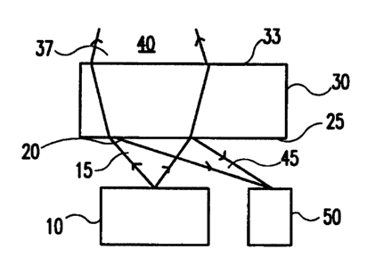
A configuration for monitoring power of an entire beam is shown in FIG. 1 a. A
light emitting device 10, e.g., a VCSEL or a light emitting diode, emits a
light beam 15
to be used in a desired application. The light beam 15 impinges upon a
diffractive
element 20, preferably on a first surface 25 of a substrate 30. The
diffractive element 20
is preferably a shallow diffractive structure, i.e., having phase depths of
less than 2n, the
depth of which is determined by the wavelength of the light emitting device 10
and the
desired efficiency of the diffractive element. Use of a shallow diffractive
structure
reduces the amount of light diffracted into the first order, i.e., into the
monitor beam.
Alternatively, this same effect may be realized may varying the width of the
step heights
so they are not equal to one another.
The diffractive element 20 transmits a majority of the beam into the zeroth or
undiffracted order to form an application beam 40, while typically
transferring a small
percentage into other orders, including a reflective order. In some
embodiments, up to
50% of the light may be deflected into higher orders to form the monitor beam.
Light
transferred into the reflective order is across the entire light beam and
forms a monitor
beam 45. Since angles associated with a reflective order to be monitored,
typically the
first reflected order, are known, an appropriately positioned monitor 50,
e.g., a
photodetector, measures the power of the monitor beam 45 and the measured
power is
-5-
CA 02306845 2000-04-18
WO 00/13051
PCTNS99/19694
then used to control the operation of the light emitting device 10 in a known
manner. A
surface 35 opposite the diffractive element may include additional optical
elements 37,
either diffractive, refractive or hybrid, for performing further optical
functions on the
application beam 40, such as collimating, focusing, and/or coupling the light
into a fiber.
As an illustrative example, if the light 15 has a wavelength of 830 nm, a
diffractive element having an eight level blazed grating made in fused silica
was
designed to have a total structure depth of approximately 2300. This depth was
chosen
so that approximately 90% of the light is transmitted into the zeroth order to
form the
application beam 40, approximately 2% of the light is reflected into the first
reflected
order to form the monitor beam 45, approximately 1.4% of the light is
transmitted into
the first transmission order, with the remainder of the light being
transferred to higher
orders in decreasing percentages.
In both Figures 1 a and 1 b, the diffractive element 20 also focuses the
monitor
beam onto the detector 50. The focusing of the monitor beam avoids VCSEL
feedback
encountered when a grating is used to simply scatter the light. Further, the
focusing
allows the detector to be smaller. In general, it is preferable that the
diffractive optical
element used in the present invention provides optical functioning, e.g.,
collimation,
focusing, to the monitor beam, particularly when the diffractive optical
element reflects
the monitor beam so no other additional surfaces are available on which to
provide an
-6-
CA 02306845 2000-04-18
WO 00/13051 PCTNS99/19694
optical element for further optical functioning to the monitor beam. Such a
diffractive
element is preferably a computer generated hologram.
As shown in FIG. lb, additionally or alternatively, a transmission diffractive
element for performing at least one of the further optical functions on the
application
beam 40 may be incorporated with the reflective diffractive element 20 to form
a
combined diffractive 22. As can be seen in FIG. 1 b, the application beam 40
is
converging after leaving the first surface 25 of the substrate 30. The
incorporation may
be achieved by multiplexing the transmission hologram for forming the
transmission
diffractive element with the reflective hologram for forming the reflective
diffractive
element, discussed below.
For a transmission hologram, the physical step height d needed to get a phase
depth of phi (~) is:
d=~.*~/{2~*(n-1)}
where n is the refractive index.
For a reflection hologram, the physical step height d needed to get a phase
depth of phi (~) is:
d=~,*~/(2*2n)
To get a phase depth of 2~, the etch depth is ~./(n-1 ) for a transmission
hologram
and ~./2 for a reflection hologram. Thus, depending on the refractive index of
the
CA 02306845 2000-04-18
WO 00/13051 PCT/US99119694
material, the reflection hologram may be much shallower than the transmission
hologram
for the same phase depth. When combining these two types of holograms, the
transmittance functions for the reflection hologram and transmission hologram
are
multiplied, i.e., their phase functions are added together. However, the phase
values for
the two types of holograms are encoded differently in accordance with the
above
equations. For example, ifthe index n=1.5, then a phase depth of 2~ for the
transmission
hologram is 2~., four times greater than the ~,/2 for the reflection hologram.
If sixteen
levels are used to encode the transmission hologram, then the four shallowest
levels will
correspond to 0, n/2, ~c and 3 n/2 for the reflection hologram.
When the phase functions are added for sufficiently low index materials, the
reflection hologram function will only be a small modulation on the
transmission
hologram function, since the depth of the reflection hologram is much
shallower; so there
is not a large effect of one function degrading the other. Indeed, when using
a plurality
of levels, often the shallower levels needed for the transmission hologram
correspond to
many of the levels needed for the reflection hologram. Of course, if needed,
either one
or both of the hologram could incorporate levels having phase depths in excess
of 2~.
An embodiment employing a transmission hologram for forming the monitor
beam is shown in FIG. 2. The light emitting device 10 again outputs a beam of
light
which is incident on a substrate 30 having a first surface 25 and a second
surface 35. The
_g_
CA 02306845 2000-04-18
WO 00/13051 PCTNS99/19694
diffractive element 5 S on the first surface deflects some light 60 off to the
side. As can
be seen .in FIG. 2, the diffractive element 55 also collimates the monitor
beam . This
additional optical functioning may be realized by simply adding the two
transmission
functions together. Such collimation insures more light will be delivered to
the detector
50 and allows greater separation between the VCSEL and detector, since the
monitor
beam is no longer expanding.
The deflected light 60 is then reflected off of the second surface by total
internal
reflection if the deflection angle is sufficiently steep, i.e., exceeds the
critical angle at the
second surface interface, or by an appropriately placed reflector on the
second surface,
such as a patch of metal 65. The reflected beam 70 then returns to the first
surface, where
it is incident on another transmission hologram 72 which focuses the monitor
beam 75
onto the detector 50.
Again, the second surface may include optical elements for performing further
optical functioning on the application beam 40. In the example shown in FIG.
2, the
further optical element 37 on the second surface 35 of the substrate 30
focuses the
application beam 40 in order to couple the light into an optical fiber 78.
The another transmission hologram 72 for focusing the deflected light onto the
detector may be omitted if the diffractive element 55 is designed to provide
focus to the
-9-
CA 02306845 2000-04-18
WO 00/1305t PCT/US99/19694
deflected light beam. Such a design would eliminate the additional loss
incurred if the
light passes through another diffractive optical element having power.
Further, as shown
in FIG. 2, the deflected light may be reflected a plurality of times if the
angle is
appropriate or if reflectors 65 are provided on the first surface of the
substrate. This
increases flexibility regarding placement of the detector. Further, as
discussed above in
conjunction with the reflection diffractive, additional optical elements may
be
incorporated with the transmission diffractive to provide further optical
functioning on
the application beam 40, either on the first surface or the second surface of
the substrate
30.
The entire system may be integrated as shown, for example, in FIG. 3a and 3b.
When the light emitting device is directly attached to a glass substrate as
shown in FIG.
3a, the configuration shown in FIG. 2 is preferred. In FIG. 3b, the light
emitting device
is attached to a second substrate 80 which is separated from the substrate by
spacer
blocks 85, resulting in sufficient room to use either power monitor
configuration. For
either of these configurations, the integration may occur on a wafer level.
As an alternative to the use of substrates, the reflection diffractive element
may
be incorporated into a plastic or glass cap 90 which may go inside a can 95
housing the
light emitting device as shown in FIG. 4. The cap forms a protective,
potentially
hermetic, seal for the light emitting device. The cap 85 may be made in many
ways,
-10-
CA 02306845 2000-04-18
WO 00/13051 PCT/US99/19694
including injection molding.
Another configuration is shown in Figure 5. A shown therein, light from the
VCSEL 15 impinges upon a diffractive element which both splits off a portion
of the
beam to form a monitor beam and collimates both the monitor beam and the
application
beam. Such collimation allows increased flexibility in placement of the
detector 10,
since the monitor beam is no longer expanding. Additionally, the diffractive
element 55
may also be used to focus the monitor beam on the detector 50. Alternatively,
a
refractive element may be provided on a surface adjacent the diffractive
element 55 to
provide the focusing. When placed near each other, i.e., the elements are
close enough
that the deflection created by the diffractive element still allows the beam
to be focused
by the focusing element, the relative order of the diffractive element and the
focusing
element doesn't matter. Preferably, the two substrates used in Figure 5 are
created and
bonded together on a wafer level and them diced in order to form the optical
system for
both the monitor beam and the main or application beam shown therein.
An example of a configuration for monitoring an array of VCSELs is shown in
Figure 6. A monitor detector is provided for at least one of the VCSELs. The
at least
one detector, typically a corresponding array of detectors, is positioned in
the plane of the
drawing and a front view of each VCSEL 10 with a corresponding detector 55
would
look like Figure 5. Again, the monitor beam may be collimated and/or focused
by the
-11-
CA 02306845 2000-04-18
WO 00/I3051 PCT/US99/19694
diffractive element. This collimation and/or focusing is particularly
important when
monitoring more than one beam of the array in order to insure the monitor
beams do not
influence one another.
Another alternative to the use of substrates, when the light is to be coupled
to a
fiber, includes incorporating the diffractive element for forming the monitor
beam in a
rod attached to the fiber.
While typically the entire beam is to be used, if only part of the beam is
used, the
diffractive element may create the monitor beam only from the portion of the
beam to be
used in the application. For example; if coupling the light to a fiber, only
the portion of
the beam which will be delivered to the core region of the fiber may be
monitored.
Although preferred embodiments of the present invention have been described in
detail herein above, it should be clearly understood that many variations
and/or
modifications of the basic inventive concepts taught herein, which may appear
to those
skilled in the art, will still fall within the spirit and scope of the present
invention as
defined in the appended claims and their equivalents.
-12-