Note: Descriptions are shown in the official language in which they were submitted.
CA 02306846 2000-04-18
WO 99/23762 PCT/US98I23285
RECONFIGURABLE RADIO SYSTEM ARCHITECTURE
BACKGROUND OF THE INVENTION
This application claims the benefit of the U.S. Provisional Applications
Serial
Number 60/064,097, filed November 3, 1997; Serial Number 60/064,098, filed
November 3, 1997; and Serial Number 60/064,132, filed November 3, 1997.
This application relates to field programmable radio frequency communications
systems in general, and more particularly to a field programmable digital
radio frequency
communications system that is field programmable in either the transmit or
receive mode
and to operate with a variety of signaling schemes.
Descriptions of the various components of the system are contained in co-
pending
patent applications owned by the assignee hereof and filed concurrently
herewith,
specifically: U.S. Patent Application S.N. , entitled "Reconfigurable Radio
System Architecture And Method Therefor"; U.S. Patent Application S.N. ,
entitled "A Control System For Controlling the Processing Data of a First In
First Out
Memory and Method Therefor"; U.S. Patent Application S.N. , entitled
"Configurable Circuits for Field Programmable Radio Frequency Communications
Equipment and Methods Therefor"; U.S. Patent Application S.N. , entitled
"A System For Accelerating the Reconfiguration of a Transceiver and Method
Therefor";
U.S. Patent Application S.N. , entitled "A Field Programmable Radio
Frequency Communications Equipment Including A Configurable IF Circuit, And
Method Therefore" ; U.S. Patent Application S.N. , entitled "A Field
Programmable Modulator-Demodulator Arrangement For Radio Frequency
Communications Equipment, And Method Therefor"; U.S. Patent Application S.N.
entitled "A-Digital Noise Blanker For Communications Systems And
entitled TCM
Methods Therefor"; U. S. Patent Application S.N. "
Revisiting System and Method"; U.S. Patent Application S.N. , entitled
"Least Squares Phase Fit As Frequency Estimate"; U.S. Patent Application
S.N. , entitled "Polar Computation of Branch Metrics For TCM"; U.S.
Patent Application S.N. , entitled "Efficient Modified Viterbi Decoder";
CA 02306846 2000-04-18
WO 99/23762 PCTNS98n3285
2
U.S. Patent Application S.N. . entitled "Receiver For a Reconfigurable
Radio System and Method Therefor"; each of which is incorporated herein by
reference.
In the use of radio frequency equipment for communications, there is a need
for of
a large a variety of types communication devices, such as receivers,
transmitters and
transceivers that are able to operate with a large variety of communications
schemes, or
waveforms such as, AM, AME, A3E, H3E, J3E, CW, SSB, M-PSK, QAM, ASK, angular
modulation, including FM, PM, FSK, CMP, MSK, CPFSK etc., as well a need of
being
able to process the signals within the communications devices, such as by
filtering, gain
control, impulse noise rejection, etc. To acheive this in the past, a
plurality of different
dedicated pieces of equipment was required, such as, receivers, transmitters
and
transceivers, each designed to operate with separate communication schemes or
waveforms, or a limited group of schemes or waveforms. Hence it would be
desirous to
have a configurable type of radio frequency communications equipment that is
readily
field programmable to function as a transmitter and receiver and to be able to
be
programmed to function with any of the above mentioned communications schemes
or
waveforms.
In the addition, quite often there is a need for portable battery operated
radio
frequency communication equipment. Hence it is desirous with battery operated
type of
equipment to make the equipment as small and as light as practical for ease of
handling,
and to reduce the power drain on the equipment battery to extend the portable
life of the
equipment.
Is therefor an object of this invention to provide a new and improved digital
radio
frequency communications equipment that can be readily configured by the user
in the
field as functioning as either a receiver or transmitter.
Is also an object of this invention to provide a new and improved type of
radio
frequency communications equipment that can be readily configured by the user
in the
field to operate with any of a plurality of communications schemes or
waveforms.
CA 02306846 2000-04-18
WO 99/Z3762 PCT/US98/232$5
3
Is also an object of this invention to provide a new and improved radio
frequency
communications equipment that can be readily configured by the user in the
field to
operate in any of a plurality of communications schemes or waveforms and
configured to
provide filtering and wave shaping parameters in accordance with the selected
communications scheme or waveform.
Is also an object of this invention to provide a new and improved radio
frequency
communications equipment that can be readily configured by the user in the
field that is
relatively light weight.
Is also an object of this invention to provide a new and improved radio
frequency
communications equipment that can be readily reconfigured by the user in the
field that is
designed to use reduced battery power to extend the life of the portable mode
of
operation.
These and other objects and advantages of the present invention will be
readily
apparent to one skilled in the art to which the invention pertains form a
perusal of the
claims, the appended drawings, and the following detailed description of the
preferred
embodiments.
CA 02306846 2000-04-18
WO 99/23762 PGT/US98I23285
4
.BREIF DESCRIPTION OF THE DRAWINGS
Figure 1 is a block diagram of a field programmable radio frequency
communications system, including a configurable digital IF subsystem, that can
be field
configured to operate in the receiver or transmitter mode of operation, the
selected
signaling scheme or waveform, and tailor the circuits with corresponding
parameters for
signal processing.
Figure 2 is an expanded block diagram of the field configurable radio
frequency
communications system of Figure 1 illustrating the interconnection of various
subsystems.
Figures 3A and 3B include a flow diagram explaining the steps involved in
configuring the field programmable radio frequency communications system.
Figures 4A and 4B include an expanded block diagram of the field configurable
radio frequency communications system showing interconnections between various
subsystems when configured in the transmit mode.
Figure 5 is a block diagram of the radio frequency sub-system portion of the
field
configurable radio frequency communications system.
Figure 6 is a block diagram of the intermediate frequency (IF) sub-system
portion
of the field programmable radio frequency communications system including
demodulation and modulation and signal processing systems, a baseband signal
processing system, and bus structure, adapted to be implemented as a applied
specific
integrated circuit device (ASIC).
Figure 7 includes a simplified block diagram of a radio frequency transceiver
including the IF sub-system
Figure 8 includes a block diagram of the field configurable digital IF sub-
system
configured as an IF demodulator and signal processing circuit for use in the
receive mode
of operation.
CA 02306846 2000-04-18
WO 99/23762 PGTNS98n3285
Figure 9 includes a block diagram of the field configurable digital IF sub-
system
configured as an IF modulator and signal processing circuit for use in the
transmit mode
of operation.
Figure 10 is a layout of the IF sub-system control registers.
Figure 11 is a block diagram of the digital IF subsystem configured as a
digital
demodulator and signal processing circuit including abbreviated digital
control
commands for programming operating parameters for various circuits for the
receive
mode of operation, signaling scheme or waveform, and signal processing
thereof.
Figure I2 is a block diagram of the IF subsystem configured as a modulator and
signal processing circuit including abbreviated digital control commands for
programming operating parameters for various circuits for the transmit mode of
operation, signaling scheme or waveform, and signal processing thereof.
Figure 13 is a block diagram of the IF subsystem configured as modulator and
signal processing circuit including abbreviated digital control commands for
programming operating parameters for various circuits for the angle modulation
for the
transmit mode of operation.
Figure 14 is a block diagram of the circuits of the backend circuits of the IF
subsystem including abbreviated digital control commands for configuring and
programming various baseband circuits for the selected mode of receiver or
transmitter
operation, and baseband signal processing.
Figure 15 is a block diagram of the system clock circuit of the IF subsystem
including abbreviated digital control commands for programming the system
clock
circuit.
Figure 16 is a block diagram of the turn around accelerator circuit of the IF
subsystem including abbreviated digital control commands for programming the
turn
around accelerator circuit.
CA 02306846 2000-04-18
WO 99/23762 PGT/US98/23285
6
Figure 17 is a block diagram of the mode registers of the IF subsystem
including
abbreviated digital control commands for programming the various circuits in
the
semiconductor chip.
Figure 18 is a block diagram of the keep alive clock circuit of the IF
subsystem
including abbreviated digital control commands for programming the keep alive
clock
circuit.
Figure 19 is a block diagram of the interrupt control circuit of the IF
subsystem
including abbreviated digital control commands for programming the interrupt
control
circuit.
Figure 20 is a block diagram of digital to analog converter interface circuit
of the
transmitter modulator configuration.
Figure 21 is a block diagram of analog to digital converter interface circuit
of the
receiver demodulator configuration.
Figure 22 is a block diagram of a gain scale control circuit of the receiver
demodulator configuration.
Figure 23 is a block diagram of a impulse noise blanker circuit of the
receiver
demodulator configuration.
Figure 24 is an expanded block diagram of the impulse noise blanker of Figure
23
including abbreviated configuration commands applied thereto.
Figure 25 is a block diagram of a log-linear and take largest of two circuit
of the
impulse noise blanker circuit of Figure 24.
Figure 26 is a block diagram of a widebaod interpolator circuit of the
receiver
demodulator configuration.
Figure 27 is a block diagram of a wideband mixer circuit of both the
transmitter
modulator and receiver demodulator configuration
CA 02306846 2000-04-18
WO 99/2362 PCT/US98/23285
7
Figure 28 is a block diagram of a wideband numerical control (NCO) circuit of
both the transmitter modulator and receiver demodulator configuration.
Figure 29 is a block diagram of a wideband decimation and compensating FIR
filter circuit of the receiver demodulator configuration.
Figure 30 is a block diagram of a wide band interpolation and compensating FIR
filter circuit of the transmitter modulator configuration.
Figure 31 is a block diagram of a CIC decimation circuit of the receiver
demodulator configuration.
Figure 32 is a block diagram of a CIC interpolator circuit of the transmitter
modulator configuration.
Figure 33 is a block diagram of a compensation FIR filter (CFIR) circuit of
the
receiver demodulator configuration.
Figure 34 is a block diagram of a compensation FIR filter (CFIR) circuit of
the
transmitter modulator configuration.
Figure 35 is an illustration of the frequency response of the CIC circuit.
Figure 36 is an illustration of the frequency response of the CFIR.
Figure 37 is an example plot of the combined operation of the CIC and CFIR
filters
Figure 38 is a block diagram of a programmable FIR (PFIR) filter circuit of
the
receiver demodulator configuration.
Figure 39 is a block diagram of a programmable FIR (PFIR) filter circuit of
the
transmitter modulator configuration.
Figure 40 is a block diagram of a gain control circuit of both the receiver
demodulator and transmitter modulator configuration.
CA 02306846 2000-04-18
WO 99123762 PGT/US98/23Z85
8
Figure 41 is a block diagram of an example of a baseband signal processing
circuit configured to include a combination of the re-sampler, the narrow band
mixer and
the Cartesian to polar converter.
Figure 42 is a block diagram of a polyphase re-sampler model of the baseband
signal processing circuit.
Figure 43 is an example plot of the aliasing stop band of the polyphase re-
sampler
model.
Figure 44 illustrates the input and output signals of the block diagram of a
Cartesian to polar converter circuit.
Figure 45 is a block diagram of an example of a baseband processing circuit
configured to include a combination of the narrow band mixer and the Cartesian
to polar
converter.
Figure 4G is an example plot of the phase accuracy of the Cartesian to polar
example of Figure 45.
Figure 47 is a block diagram of a narrow band complex mixer circuit of the
baseband signal processing arrangement.
Figure 48 is a block diagram of the combined narrow band NCO and narrow band
complex mixer circuits of the baseband signal processing arrangement.
Figure 49 is a block diagram of FIFO de-tagging arrangement.
Figure 50 is a block diagram of the turnarround accelerator and flush and
queue
arrangement.
Figure 51 is a block diagram of the receiver demodulator configuration for use
in
the flush mode.
Figure 52 is a block diagram of an interrupt service functional block diagram.
Figure 53 is a process for calculating the configuration changes to be make in
the
IF ASIC, checking the changes, and loading the changes into memory.
CA 02306846 2000-04-18
WO 99/23962 PCT/US98/23285
9
Figwes 54A and 54B include an expanded process for the selecting configuration
changes steps of Figure 53.
Figures SSA and SSB include a block diagram of the field programmable radio
frequency communications system configured as a FM voice transmitter.
Figures 56A and 56B include a block diagram of the field programmable radio
frequency communications system configured as a FM voice receiver.
Figwes 57A, 57B and 57C include a block diagram of the field programmable
radio frequency communications system configured in a receiver mode for single
sideband, AME and A3E signaling schemes.
Figures 58A and 58B include a block diagram of the field programmable radio
frequency communications system configured in a transmitter mode for single
sideband,
AME and A3E signaling schemes.
Figwe 59 includes a block diagram of the IF subsystem configured to function
with the receiver block diagrams of Figures 57A , 57B and 57C.
Figure 60 includes a block diagram of the IF subsystem configured to function
with the transmitter block diagrams of Figures 58A and 58B.
Figures 61 A and 61 B include a flow diagram for explaining the operation of
Figure 49.
Figwe 62 includes a buffered arrangement for the IF ASIC.
DESCRIPTION OF PREFERED EMBODIMENTS
The invention uses an IF (carrier based) digital multi bit signal processing
circuits
to implement field programmable digital processor type of radio frequency
communications functions in configurable hardware under control of a field
programmable radio communications system, or a computer. Carrier based, as
used
herein, means that the signals can be processed at a system intermediate
frequency, or at
the RF system carrier frequency, although the invention is to be described
herein as
operating at the intermediate frequency.
CA 02306846 2000-04-18
WO 99/Z3762 PCT/US98/23285
1 ) Field Programmable Radio Communications Svstem Description
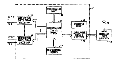
Figure I describes a field programmable radio frequency communications system
that can be programmed by a user to form a digital signal processing system 10
that is
adapted to be coupled to a radio frequency receiver and or transmitter
subsystem 12 to
configure a radio frequency receiver and/or transmitter system to operate with
any of a
plurality of radio frequency waveforms or signaling schemes, such as, AM, AME,
A3E,
H3E, J3E, CW, SSB, M-PSK, QAM, ASK, and angular modulation, such as, FM, PM,
FSK, CMP, MSK, CPFSK etc. The mufti bit digital instructions, commands and
software
configure the digital processing system 10 can be provided from a remote
location or
stored in a configuration non-volatile memory 14. When using the memory 14,
instructions are down loaded into the memory 14 from the configuration input
circuit 16
under the control of the configuration control system 18. In response to
instructions
provided from the user input circuit 26, the configuration control system 18
{in response
to instructions or commands stored in the configuration memory 14) connects
selected
ones of a plurality of ccinfigurable digital signal processors (CDSP) 20 and
22, and
configures the digital IF subsystem 24 in a receiver or transmitter mode of
operation with
the radio frequency subsysteml2 to function in accordance with the signaling
scheme
selected by the user. Hence, the arrangement is such that a single piece of
equipment can
be, in response to instructions from the user, configured to operate with a
radio frequency
subsystem 12 as a substantially universal type of radio frequency
communications
system, controlled the configurations inputted directly yr loaded into the
configuration
memory 14.
As illustrated in Figure 2, the conf guration control system I 8 includes a re-
programmable processor subsystem A (which, for example, can be the central
control
digital signal processor [BIOP] 28), coupled to the radio configuration
download port 16,
the re-programmable keyboard display unit (KDU) or computer (CPU) 26, the
architecture configuration storage device (which can for example be a large
memory 14),
and a re-configurable hardware element A (which, for example can be the
central control
field programmable field array [CFPGA] 30). The central control CFPGA 30 is
also
CA 02306846 2000-04-18
WO 99123762 PGT/US98123285
11
coupled to a re-programmable processor subsystem E (which, for example can be
the
control digital signal processor (CDSP] 32), the intermediate frequency (IF)
subsystem
which is a configured as a digital IF modulator or demodulator and
configurable
baseband signal processing system ( which, for example, can be in the form of
an
application specific integrated circuit [ASIC] 24), the configurable digital
signal
processor 20 and the configurable digital signal processor 22. The IF
subsystem 24 is
coupled to the radio frequency subsystem 12 and is configured to provide
modulated IF
signals to a transmitter, or to receive RF signals to be demodulated.
The configurable digital signal processing circuit 20 includes a re-
programmable
processor subsystem B (which, for example can be the auxiliary digital signal
processor
[ADSP] 34) that is coupled through a re-configurable hardware element B
(which, for
example can be the auxiliary FPGA [AFPGA] 3G) to the CFPGA 30. The
configurable
digital signal processing circuit 22 includes a re-programmable processor
subsystem C
(which for example can be the voice/data DSP [VDSP] 38) that is coupled
through a re-
configurable hardware element C (which for example can be the voice/data FPGA
[VFPGA] 40) to the CFPGA 30. The configurable digital signal processing
circuit 22
also includes a re-programmable processor subsystem D (which, for example can
be the
security processor system [SDSP] 42) that is coupled through a re-configurable
hardware
element D (which, for example, can be the security FPGA [SFPGA] 44) to the
CFPGA
30. Although the hardware elements A,B, C, and D are identified as field
programmable
gate arrays (FPGA), the hardware elements can also include a variety of signal
processing
circuits. Although the digital signal processing system 10 includes a specific
combination of interconnected re-programmable processor subsystems, re-
configurable
hardware element, architecture configuration storage device, and intermediate
frequency
subsystem, such elements and equivalents thereof could be used in various
other
arrangements and still include the inventive concepts of the digital signal
processing
system.
The BIOP 28 is the main control system which controls the loading of the
configuration multi bit commands, operating parameters and configuration
software from
CA 02306846 2000-04-18
wo 99n3~6z rcr~rs9sn3zss
12
memory 14 (or directly from a remote input) into the various subsystems of the
digital
signal processing system. It also functions as the interface to the user ICDU
26 and down
load port 16. The CFPGA 30 is the main interconnect unit involved in
configuration of
the digital signal processing system for receiver or transmitter modes of
operation and to
tailor the system 10 for the particular signaling scheme ar waveform selected.
As the
central control element, the CFPGA can be configured to provide two levels of
control, ie
the software level and the circuit (hardware) function processes, command
signal flow,
and interconnect. The CFPGA 30 can also include a variety of digital signal
processing
circuits, such as, for example, active signal processing circuit, (such as, a
veterbi decoder,
RF AGC, peak sample registers, transmit gain, thermal cut back, etc.) as well
as
providing inter processor communications ( such as, reading signals in and out
of the IF
ASIC 24, and assigning control values to various subsystems).
All other FPGAs in the system can also be configured to include mufti bit
signal processing circuits. The CDSP 32 functions with the BIOP 28 to operate
the
system once configured. The VDSP 38 can, for example be configured to process
mufti
bit digital voice and data samples, or signals for the selected signaling
scheme or
waveform. The VDSP 38 be programmed to include specific signal processing
functions,
such as, voice or data compression. The SDSP 42 can be programmed and
connected in
the system 10 to provide a special functions, such as, for example voice and
data
encryption. The IF ASIC 24 can be programmed to be configured to provide the
demodulation function for mufti bit digital signals in the receive mode, the
modulation
function in the transmit mode, and to provide mufti bit digital signal
baseband signal
processing. The various radio configurations are down loaded into the memory
14 from
the download port 16 (or directly inputted from a remote source) under the
control of the
BIOP 28. If configuration are loaded into the memory 14, all the user needs to
do is to
select the receiver or transmitter mode of operation, the signaling scheme or
waveform,
along with other communications system parameters, push the enter button, and
the
digital signal processing system 10 will automatically configure to the
desired 1tF
CA 02306846 2000-04-18
WO 99/Z3762 PCTNS98J23285
13
communications system for the user selected mode of operation. If the
configuration is
directly inputted, the system instruction are directly inputted.
The flow diagram of Figure 3 describes the various steps involved in
configuring
the radio frequency communications system. In step 48, the radio operator
enters a
change of mode of operation in the KDU 26. The BIOP 28 processes the KDU 26
information and displays text on the KDU screen (step SO) and determines if
the mode
requires FPGA changes and/or processor software changes (step 52). If not ,
the radio
communications system keeps operating unchanged (step 54). If changes are
needed, the
BIOP 28 puts the radio communications system in the idle mode (step 56). A
determination is made if the CFPGA 30 is to be changed (step 58). If so, the
BIOP 28
loads the new multi bit commands or code from the memory 14 into the CFPGA 30
(step
60). A check is made if the load is complete (steps 62, G3 and 64).
If the step 58 determines that a CFPGA 30 changes is not required, or the new
muilti bit code is successfully loaded (step 62), then a determination is made
if the CDSP
32 software requires change (step 66). If so, the BIOP 28 loads the new
software in the
CDSP 32 (step 68) and a check is made if the load is complete (steps 70, 72
and 74). If
the step 66 determines that a CDSP 32 change is not required, or the new code
is
successfully loaded (step 70), then a determination is made if the AFPGA 3G
requires
change (step 76). If so, then the BIOP 28 loads the new code in the AFPGA 36
(step 78)
and a check is made to verify that the load is complete (steps 80, 82 and 84).
If the step 76 determines that a AFPGA 3G change is not required, or the new
code is successfully loaded (step 80), then a determination is made if the
ADSP 34
requires a software change (step 86, Figure 3B). If so, then the BIOP 28 loads
the new
software in the ADSP 34 (step 88) and a check is made if the load is complete
(steps 90,
92 and 94). If the load of step 90 is complete, or no change is required, then
the BIOP 28
sends commands to the VDSP 38 and SDSP 42 to configure the DSPs for the new
mode
and a check is made to verify that the load is complete {steps 90, 92 and 94).
CA 02306846 2000-04-18
WO 99/23762 PCT/US98n3Z85
14
. At this time the process separates into three branches. In branch B the step
98
determines if the VFPGA 40 requires a change. If not, step 100 initializes the
VDSP 38
and step 102 notifies the BIOP 28 that the VDSP is ready. If the VFPGA 40
needs a
change, the step 104 has the VDSP 38 load new code into the VFPGA 40. The
steps
I06, 108, and 110 monitor to determine if the new code load in the VFPGA 40 is
complete and allows the step 100 to initialize the VDSP 38. In branch C, step
112
initializes the SDPS 42 and the step 114 tells the BIOP 28 that the SDSP 42 is
ready.
In the main branch of the process, in step 116 the BIOP 28 checks the status
of the
VDSP 38 and the SDSP 42. If the step 118 determines that the VDSP and/or the
SDSP
are not ready, the step 120 delays the process until the VDSP and the SDSP are
ready.
Thereafter the BIOP 28 initializes the system. Once the system initialization
is complete,
in the step 122 the CDSP 32 initializes the IF ASIC 24. Thereafter, the step
124 indicates
the radio frequency communications system is now in operation in the new user
selected
mode.
Figures 4A and 4B illustrate the interconnection of the various subsystems of
the
digital RF communications system interconnected to operate in a coded transmit
mode.
All the subsystems are interconnected by a data 111, address 113 and control
115 bus. In
addition, some subsystems are interconnected by a serial data bus 117. The DSP
type
subsystems 28, 32, 34, 38 and 42 include signal and control processing
arrangements
including RAM memory 121 and a digital signal processor DSP 123 or
microprocessor
119. In addition the DSP type subsystems 28, 32, 34 and 38 include
input/output devices
109. The SDSP 42 includes encryption devices I01. The VFPGA 40 is configured
to
include a FIFO 105 register, while the SFPGA 44 is configured to include a
UART 107.
The multi bit signals to be transmitted are inputted into the VDSP 38,
encrypted by the
SDSP 42, and coupled through the SFPGA 44, the VFPGA 40, the CFPGA 30, the
CDSP
32, the IF ASIC 24 and the radio frequency subsystem 12 in the transmit mode
of
transmission via the antenna 11.
Figure 5 illustrates the receiver section 125 and the transmitter section 126
of the
radio frequency subsystem 12. The receiver section 125 includes a tuner 127, a
down
CA 02306846 2000-04-18
WO 99/23762 PCT/US98/23285
converter 128 for converting the radio frequency modulated signals to
intermediate
frequency modulated signals and a analog to digital converter 129 for
outputting received
IF signals as multi bit digital samples or signal to the IF ASIC 24. The
transmitter
section 126 includes a digital to analog converter 130 for converting mufti
bit digital IF
modulated samples or signals received from the IF ASIC 24 into analog form.
The
analog signals are applied to an up converter 131 for converting the IF
modulated analog
signals to RF modulated analog signals which are amplified by a power
amplifier stage
132 and applied to the antenna 11 via a coupler circuit 133.
The IF subsystem 24 is embodied in a semiconductor chip in the form of an
application specific integrated circuit (ASIC) to provide in field
programmable
semiconductor hardware the mufti bit digital demodulation, modulation and
signal
processing functions for transceivers, capable of being configured into
digital receiver or
transmitter modes of operation, and employing various types of selected
signaling
schemes or waveforms, and configured to select operating parameters for the
various
circuits therein to conform to the selected mode of operation. The advantage
of processor
configurable functions created in the hardware of an ASIC, rather than totally
in software,
is that the configurable hardware of the ASIC requires less physical space and
consumes
less power than software running on general purpose processors running DSP
algorithms.
This is because the configurable ASIC hardware can be designed to be optimized
in its
performance.
The IF ASIC 24 can be the flat pack manufactured by Gray Chip Electronics. As
illustrated in Figure 6, the IF ASIC 24 includes a front end portion 134, a
backend portion
135, control registers 136, a bus manager 137, and an interface138. The front
end
portion 134 includes a plurality of circuits, responsive to digital commands,
that can be
selected and interconnected, along setting operating parameters, as a
configured mufti bit
digital IF modulator and signal processing circuit 152 for use in the transmit
mode of
operation, and as a configured mufti bit digital IF demodulator circuit and
signal
processing circuit 150 for use in the receive mode of operation. The IF ASIC
24 has
several mufti bit digital baseband signal processing circuits included in the
backend
CA 02306846 2000-04-18
WO 99/Z3762 PGTNS98/23285
16
portion 135, that can be configured in various ways, for processing the
baseband signal
input in mufti bit digital form to the configured IF modulator 152 in the
transmit mode,
and for processing the baseband output signals in the mufti bit digital form
from the
configured IF demodulator 150 in the receive mode, depending on the type of
signaling
scheme or waveform selected by the user. The various circuits of the IF ASIC
24 are
configurable by mufti bit digital commands from the control registers 136 or
directly
from the memory 14. The digital commands in the control registers 136 are down
loaded
from the configuration memory 14 when the digital communications system is
configured.
In the configured transmitter mode of operation, the IF ASIC 24 receives mufti
bit digital signals or samples to be transmitted via the FIFO 204. Digitally
modulated
carrier based (IF) output signals from the IF ASIC 24 are outputted to the
radio frequency
subsystem 12. In the configured receiver mode of operation, the IF ASIC 24
receives
carrier based (IF) modulated mufti bit digital signals or samples from the
radio frequency
subsystem 12 and outputted via the FIFO 204. The back end portion 135 includes
a
narrow band NCO and mixer 200, a re-sampler circuit 202 including a polyphase
re-
sampler and a re-sampling NCO, a FIFO register 204 having primary and
secondary
portions, and a Cartesian to polar conversion circuit 206, all of which are
connected to the
bus 139.
The IF ASIC 24 may, for example, accept 16 bit input samples at rates up to S
MSPS in the receive mode and generate 16 bit output samples at rates up to 5
MSPS in
the transmit mode. The minimum sample rate may, for example, be 100KSPS. The
IF
ASIC 24 is register based to allow access to the individual signal processing
blocks in
that all the various configurable circuits are connected to receive mufti bit
commands
from the control registers 136
By field programmable, it is meant that the configuration of the IF ASIC 24
can
be modified by the user at any time, not only as a transmitter or receiver,
but also as to
the type of signaling scheme or waveform involved and the parameters by which
the
signals are processed. The IF ASIC 24 is able to be configured to provide
signal schemes
CA 02306846 2000-04-18
WO 99/Z3~62 PGT/US98/23285
17
or waveforms, such as, but not limited to, complex demodulation (quadrature IF
down
conversion); data rate decimation to reduce the IF sample; narrowband
filtering; AM,
AME, A3E, H3E, J3E, CW, SSB, M-PSK, QAM, ASK, and angular modulation, such as,
FM, PM, FSK, CMP, MSK, CPFSK etc., symbol re-timing; and impulse noise
blanking
(to reduce impulsive noise), complex modulation (data rate interpolation to
raise
narrowband sample rate to the IF sample rate); IF carrier generation to place
the IF
anywhere within half the wideband sample rate; such as for SSB, CW, 2ISB, AME,
FM,
QAM, AM, M-ary PSK etc.; data shaping and narrowband filters to spectrally
limit the IF
modulation; and linear sampled data gain scale control (GSC). The IF ASIC 24
can
provide multiple output for various signal schemes or waveforms, such as, I
and Q and
phase and magnitude.
In Figure 7, the IF ASIC 24 is connected in a simpler transceiver system
wherein
the configuration of the IF ASIC 24 is controlled by a configuration processor
99
pursuant to instructions from the configuration input circuit 97. The received
digital
output signals in mufti bit form from the IF ASIC 24 are applied to the output
digital to
analog converter 103. Input signals to be transmitted are received in mufti
bit form by the
IF ASIC 24 via the analog to digital converter 101. The IF ASIC and the radio
frequency
communciations system including the IF ASIC described herein is the subject of
a
separate patent application filed concurrently herewith.
2) Receiver Demodulator Block Dial
Although the receiver section 150 and the transmitter section 152 are
described
herein as separate circuits for purposes of simplying the explanation, it
should be
understood that both the receiver and the transmitter sections are
configurable that
include a plurality common circuits, that in response to digital commands, can
be
interconnected in the form of a demodulator, a modulator and corresponding
signal
processing circuits.
CA 02306846 2000-04-18
WO 9913762 PCT/US98/23285
18
As illustrated in Figure 8, the IF ASIC 24 includes the various configurable
circuits for use in the receiver mode of operation for the above mentioned
signal signaling
schemes or wavforms, as selected by the user. The configured receiver
demodulator and
signal processing circuit 150 includes a multi bit digital signal path
consisting of an
analog to digital converter interface 154, a gain scale control 156, an
interpolator circuit
157, an impulse blanker 158, a mixer circuit 159 including a wideband inphase
and
quadrature mixers 160I and 160Q, a wideband numerical controlled oscillator
(NCO)
164 (including a offset frequency and phase shift control circuit165 and a
numerical
controlled oscillator [NCO] 167) and also inphase and quadature signal
processing
circuits each including an up-down sampler and filter circuit 169 which
includes a CIC
decimation circuit 170 I or 170 Q, a compensating filter 172 I or 172 Q, a
programmable
filter 1741 or 174Q and a gain circuit 176I or 176Q, respectively. The multi
bit digital
outputs of the PFIR circuits 174I and 174Q are connected to the backend bus
139 via the
IF gain circuits 179I and 179Q.
3) Transmitter Modulator Block Diag~
As illustrated in Figure 9, the IF ASIC 24 includes the various configurable
circuits for the transmitter mode of operation for the above mentioned signal
signaling
schemes or waveforms as selected by the user. The configured transmitter
section 152
includes a mufti bit digital input signal processing path I81 consisting of an
inphase and
quadarture down and up sampling and filter circuits each including a
programmable filter
(PFIR) 180I or 180Q receiving input mufti bit signals from the bus 139 via the
IF gain
circuits 183I and 183Q, gain circuits 182I or 182Q, a compensating filter
(CFIR) 184I or
184Q, a CIC interpolation circuit 186I or 186Q. The mufti bit output from the
OR gates
185I and 185Q connect the output of the gain circuits 182I and 182Q to mixer
circuit 187
which includes a wideband NCO 192 including a offset frequency and phase shift
control
circuit193 inphase and quaduature mixers 188I and 188Q and a NCO 195, a
modulator
adder 194, and a digital to analog interface output circuit 196. If the
circuit is configured
to function a FM or phase modulator, the mufti bit output signals from the
gain control
CA 02306846 2000-04-18
WO 99/23762 PCT/US98n3285
19
182 I are routed through the gate 191 in case of FM modulation and through
gate 193 in
the case of phase modulation.
As previously mentioned, the receiver section 150 and the transmitter section
152
are configurable in response to digital commands into the corresponding
demodulator and
modulator circuits which involves the interconnection of various common
circuits into
the selected circuit configuration. The common circuits that can be
interconnected and
configured into both de-modulator and modulator modes of operation include the
wideband mixers 1601, 160Q, 188I and 188Q, the decimator and interpolator
circuits
1701, 170Q, 186I and 186Q, the gain circuits 176I, 176Q, 182I and 182Q, the
CFIR 172I,
172Q, 184I and 184Q, the PFIR 174I, 174Q, 180I and 180Q, the IF gain 179I,
179Q,
1831 and 183Q, the NCO 167 and 195 and the frequency word, phase offset 165
and 190.
4) Control Resisters and Commands
Figure 10 includes a layout of the various registers included in the control
registers 136. The register address mapped is divided into four 256 16-bit
blocks
consisting of configuration lock (CL) 122, mode lock (ML) 114, double buffered
(DB),
and double buffered (-S; M) register types 124 and PRIR coefficients (ML) 126.
Within
the blocks, registers are further subdivided into two 128 16-bit pages (for
compatibility
and ease of programming by external processors). The mode registers contain
the bits for
the mufti bit digital commands that perform the following functions: IF ASIC
24 reset
both core and clock reset), enable internal self test bit, transmit and
receive mode bit, start
acceleration mode, wideband interpolator zero insert, and back end clock
decimation
(used to reduce the clock rate to the back end functions).
The names of the various mufti bit digital commands of the registers and their
abbreviations are listed in Table 1, including the address number, the type of
register, and
the configuration values (decimal) column and the configuration values (HEX)
column
contain the values in the control registers 136 for configuring the IF ASIC 24
in the
transmit configuration for a 20K wideband FSK system.
CA 02306846 2000-04-18
WO 99/Z3762 PGT/IIS98n3285
TABLE 1
Register Register Configuration
Long Names Short Names Value (HEX)
CLOCK GEN CGEN OXOOF8
KEEP ALIVE KEEP 0X0000
IO CTL IOC OXOSC 1
WB RAMP WRMP OXOOOA
NCO CONFIG NCOC 0X0085
CIC FACTOR CIFC 0X0004
FIR CONFIG FIRC 0X0071
NB RAMP MRMP OXOOOA
CART RES ID CRID 0X0080
FIFO CLTA FCTA 0X0000
FIFO CLTB FCTB 0X0800
MODE MODE 0X0000
BLK COUNT BCNT 0
BLK LONG AVE BIGA OXOOOC
BLK DUR THRESH BDTH OX7FFF
BLK THRESH BTH OX7FFF
BLK LONG VALUE BIGV 0
BLK SHORT AVE BSHT OXOOOC
BLK DUR GAIN BDGN 0X0000
CA 02306846 2000-04-18
WO 99/23762 PCT/US98n3285
21
BLK ENABLE BEN 0X0002
WNCO CNTR FREQ_S WCFS 0X0000
WNCO CNTR FREQ M WCFM OXFC00
WNCO OFST FREQ WOF 0X0000
WNCO OFST PH WOP 0X0000
NNCO CNTR FREQ_S NCFS OX2C3D
NNCO CNTR FREQ_M NCFM 0X0054
NNCO OFST FREQ NNOF 0X0000
NNCO OFST PH NNOP 0X0000
ID O IDO 0
ID * ID1 0
ACCEL COUNT ACNT 0X07CF
LOCK LOCK 0X0000
ISR ISRA OXOOFF
IMR IMRA 0X0070
WB CHECKSUM WCHK 0
IF GAIN GAON OX7FC 1
PRI FIFO IFIF 0
SEC FIFO GFIF 0
NB CHECKSUM NCHK 0
FIFO COUNT FCNT 0
FIFO THRESH FTH OXOOOA
RNCO DECIMATE F RSDF 0X0000
CA 02306846 2000-04-18
WO 99/23762 PCT/US98n3285
22
RNCO DECIMATE I RSDI 0X0080
RNCO ADJUST RSAD 0X0000
INPH MIXER REG IPMR 0X0000
QUAD MIXER REG QPMR 0X0000
TAGVAL 0X0000
5) Receiver Demodulator and Transmitter Modulator with Abbreviated Commands
Figure 11 includes the various processing circuits of the configured receiver
circuit 150 with various mufti bit command signals from the control registers
136 being
applied thereto (as indicated by the various abbreviated commands in the
dashed blocks
and designated with the letters CR). However the embodiment of the configured
receiver
section 150 of Figure 11 includes wideband interpolator circuits 162I and 162Q
after the
inphase and quadrature mixer 160I and 160Q instead of before the mixers of
Figure 8
Figure 12 includes the various processing circuits of the configured
transmitter
circuit 152 with various mufti bit control command signals from the control
registers
being applied thereto (as indicated by the various abbreviated commands in the
dashed
blocks and the letters CR adjacent to the command line). However, the
embodiment of
Figure 12 includes the IF gain circuits 182 I and 182 Q between the PFIR
filters and the
CFIR filters instead of to the bus 139 of Figure 9.
6)AJn ale Modulator
The angle modulator described herein is the subject of a separate patent
application filed concurrently herewith.
Figure 13 includes a block diagram of the configured modulator circuit 152 of
Figure 12, with abbreviated mufti bit commands from the control registers
applied to
various circuits, illustrating how the modulator circuit is configured to
operate with angle
CA 02306846 2000-04-18
WO 99/23762 PCT/US98/23285
23
modulation, such as CPM, FM, PM, MSK and CPFSK. Although, the block diagram of
Figure 13 is more specifically described with regard to FM and PM, the
concepts will
apply to all types of angle modulation. Only a portion of the configurable
modulator
circuit 152 is used for angle modulation. Only that portion of the dual paths
marked I are
used, and that marked Q is not. The multi bit signal or samples, such as 16
bit digital
signals, to be transmitted, are applied via the FIFO 204 at a 8K clock rate to
the PFIR
180I. An 18 bit signal is outputted from the PFIF 180I at a 16K clock rate to
the gain
scale 182I, which provides a 16 bit signal at the 16K clock rate. The CFIR
184I outputs
the input from the gain scale at 18 bits at a 32K clock rate to the CIC
interpolator and
scale factor circuit 186I, which in turn provides a mufti 18 bit signal at a
960K clock rate.
Depending if the FM or phase modulation is to be used, the offset frequency
gate
191 or offset phase gate 193 is enabled. In such case, 18 bit digital signals
at the 960K
clock rate are applied to the wideband offset frequency shift circuit 197 or
the wideband
offset phase shift circuit 199, respectively. A 28 bit signal at the 960K
clock rate is
applied from either the offset frequency shift circuit 197 or the offset phase
shift circuit
199 are applied to the wideband NCO 195 to frequency, or phase, modulate the
NCO
about the programmed NCO center frequency. Only the COS output from the NCO
195
is allowed to pass to the wideband mixer adder 194 as a modulated 18 bit
signal at the
960K clock rate and outputted via the DAC interface 196. This arrangement has
the
particular advantage of allowing the FIFO 204 to operate at a low sample rate
(such as
8K) for all types of modulation and demodulation schemes, while the up sampler
and
filter circuits 181 can be used to increase the signal sample rate to the IF
center frequency
(960K) for the angle modulation scheme as described..
7) Block Diagrams of Backend
Figure 15-19 includes the various processing circuits of the backend section
135
with various control command signals from the control registers 136 being
applied
thereto (as indicated by the various abbreviated mufti bit commands in the
dashed blocks
and designated as CR). Figures 15, 16, 17, 18 and 19 are the various other
processing
circuits including the system clock 210, turns around accelerator 212, the
mode registers
CA 02306846 2000-04-18
WO 99/23762 PGT/US98123285
24
214, and the keep alive clock 218 with various control command signals from
the control
registers 13G being applied thereto (as indicated by the various abbreviated
commands in
the dashed blocks).
8) Digital to Analo Cg onverter Interface
A block diagram of the of the digital to analog converter (DAC) interface
circuit
154 in the configured transmitter circuit 152 is illustrated in Figure 20. The
DAC
interface circuit includes a numerical conversion circuit 230 and an output
register 232.
The inputs to the interface 154 are the sample output enable and carrier based
modulated
data. The sample output type is controlled by the processor and is parallel
numeric
formatted data.
A block diagram of the of the analog to digital converter (ADC) interface
circuit
154 in the configured receiver circuit 150 is illustrated in Figure 21. The
ADC interface
circuit 154 includes a rising edge sampling register 236, a falling edge
sampling register
238, a synd register 240, a mux 242, a bit select 244, a bit select and delay
24G and a
numeric conversion 248.
The ADC interface 154 accepts 12 to 16-bit data samples multiplexed with 4 to
O-
bit gain index values. ADC value bits that are not used should be tied low.
The data is
registered on both the rising and falling edge of the receive clock as
selected by the
configuration processor for input into the numeric conversion sub-functions.
The ADC
interface 154 shall provide weak internal pull-downs to logic '0' allowing for
data widths
less than a preset number of bits to be zero extended. Following the
registering of
samples, the input sample data numeric format as programmed by the
configuration
processor is converted to the internal numeric data. Attenuation indexes to
the IF ASIC
24 are selected by the configuration processor. A n-bit Gain Delay (GAIN DLY)
0 <_
Gain Index 5 GAIN_BITS value shall allow for programmable delays for alignment
of
the gain into the GSC. The n-bit Gain Index (Gi) shall be time delayed within
the ADC
interface 154 to align Gi with the sample data. The inputs to the ADC
interface 154 is the
gain delay as configured by the processor and the data/gain index. The sample
input type
CA 02306846 2000-04-18
WO 99123762 PCT/US98123285
and the sample register select are also configured by the configuration
processor. The
output includes the gain index value and the ADC data.
The configuration commands applied to the ADC interface 154 are listed in
Table
2.
TABLE 2
Re ister IO CLT (IOC)
Command Description
SMPL INP TYPE Receive - type of AID converter, selects
sample input numeric format of conversion
to internal data format.
Command Description
SMPL REG_ SEL Selects rising or falling edge sample
Command Description
GAIN BITS Selects the number of least significant bits
input to the gain scalar
Command Description
GAIN DLY Delay gain compensation by n samples
Command Description
SMPL OUT TYPE Transmit - selects conversion of internal
numeric formatted data to DAC format
9) Gain Scale Control
Figure 22 includes a block diagram of the gain scale control (GSC) circuit 1
SG in
the configured receiver circuit 1 SO including a multiplier 250. The purpose
of the GSC
CA 02306846 2000-04-18
WO 99123762 PCT/US98I23285
26
circuit 156 is to correct the input sample data for external attenuation. This
is
accomplished by passing the sample data through the 2"-ga'"B"~ multiplier 250.
The GSC
circuit 156 accepts n-bit data from the ADC interface 154. Prior to entering
the IF ASIC
24, the sample data has been adjusted by a modulo 2 attenuation supporting
zero to four
steps. For example, if a 12 bit A/D is used then the data outputs of the A/D
are attached
to the MSB of 16 bit inputs. The l2bit number is sign extended and scaled by
2'~A~N B~Ts
to put it into the LSB of the 16 bit word. Lastly, the value is shifted up by
the Gain
Index. The input to the GSC circuit 56 is the gain index from the analog to
digital
converter and the output is gain controlled data to the impulse blanker
circuit 158.
10) Adder
The adder 194 of the configured transmitter circuit 152 accepts inputs from
the in
phase and quadrature phase components of the modulator mixers 188I and 188Q.
The
inputs are added together and outputted in real form to the DAC interface 196:
11) Impulse Noise Blanker
The impulse noise blanker circuit and the exponential averaging circuit
described
herein are the subjects of a separate patent application filed concurrently
herewith.
Figure 23 includes a block diagram of the impulse blanking circuit 158 used in
the
receive mode of operation. The purpose of the impulse noise blanker 158 is to
prevent
impulse noise from ringing the narrowband filters downstream with high energy,
short
duration, impulse noise. The input noise blanker 158 uses mufti bit digitized
signal
samples. The method of comparison used for noise blanking is to compare energy
that is
around for a long time to energy of short duration. Radio frequency noise can
be
characterized as short term wide bandwidth energy while signals of interest
can be
characterized as long term limited bandwidth energy. Signal of short duration
compared
to the signal of interest is assumed to be impulse noise and is to blanked. A
long term
average energy is made and compared to the short term average energy. The
absolute
value of the signal is used as an approximation for the signal energy. The
difference
between the long term average energy and the short term average energy is used
as a
decision metric and is compared to a threshold and a blanking decision is
made. The
CA 02306846 2000-04-18
WO 99/23762 PGT/US98/23285
27
threshold of the blanking period is dependent upon the characteristics of the
selected
signaling scheme or waveform. For example, the threshold for FSK can be set at
a low
level while the threshold for SSB is required to be set at a higher level. The
duration of
the blanking period is set to approximate the impulse ringing characteristics
of the radio
system filters, as configured.
The impulse noise blanker circuit 158 is configured by multi bit commands from
the control registers 136 which have received instructions from the memory 14
approximating the impulse noise ringing time of the analog filters in the
system. The
digital IF input signals are applied to a digital signal delay circuit 256
because of the
delay in the averaging process, the signal itself is held in a digital delay
line so that the
actual samples that cause the blanking decision can them selves be blanked. As
illustrated
in Figure 23, the mufti bit digital IF input signal including the noise
impulse therein is
applied to a blanker gate 257. The control line of the blanker gate 257 is
connected to
receive the blanking signal from the noise detection and processing circuits
to actuate the
gate to substitute "0" signals from the blanking signal generator 258 for the
digital IF
input signal during the duration of the blanking signal.
The digital IF input signals including the impulse noise thereon is also
applied to
a short delay and short exponential averaging circuit 259 which provides an
output signal
representative of the average magnitude of the short duration noise impulses,
and are also
applied to a long average exponential averaging circuit 260, which provides
and output
signal representative of the average magnitude of the input signal. An
additional delay
line is included before the short energy averaging circuit 259 to align its
output to those
of the long averaging circuit 260 which has a larger delay so that the outputs
from both
the circuits are approximately in synchronized in time when applied to a
difference circuit
262. The difference circuit 262 subtracts the magnitudes of input signals and
applies the
difference to a threshold on circuit 264. Simultaneously the difference signal
is also
applied to a exponential blanking exponential duration circuit 266. When the
difference
signal exceeds the threshold level (indicating the presence of a noise
impulse) a signal is
applied by the threshold on circuit 264 to the threshold gate 267 which in
turn activates
CA 02306846 2000-04-18
WO 99163762 PCTNS98/23285
28
the exponential blanking duration circuit 266 to receive the difference signal
and initiate
the generation of the duration signal based upon the magnitude of the
difference signal.
The duration of the blanking period is determined by setting the gain of the
exponential
decay circuit 266 and setting the duration level of the threshold duration
circuit 268. The
output of the exponential blanking circuit 266 is applied to a threshold
duration circuit
which provides a blanking signal to the blanking gate 257 which in turn blanks
the digital
IF input signal as long as the input from the threshold duration circuit 266
exceeds the
threshold level.
The difference signal is also applied to a threshold large impulse detection
circuit
269 which compares the magnitude of the output of the exponential blanking
duration
circuit 266 to the magnitude of the difference signal. If after a blanking
sequence has
been initiated a second noise impulse is received, and if the difference
signal resulting
from the subsequent noise impulse is less than the output from the exponential
blanking
duration circuit 266, the prior blanking sequence continues without change. If
the
difference signal resulting from the subsequent noise impulse is greater than
the output of
the exponential blanking duration circuit 266, the threshold large impulse
detection
circuit 269 reactivates the threshold gate 267 to enable the exponential
blanking duration
circuit start another blanking duration sequence based upon the magnitude of
the
difference of the subsequent noise impulse.
The impulse noise blanker 158 utilizes exponential smoothing in the short
averaging circuit 259, the long averaging circuit 260 and in the exponential
blanking
duration circuit 266 to provide an equivalent N-period moving average where N
= (2/oc)-
1. A smoothed signal is created based on weighted samples and previous values
then
compared against the present sample to generate an error signal.
A log function circuit 272 compresses input data and maps the data into the
log2
domain. This allows the register sizes and signal paths in the exponential
smoother
circuits to be small without reducing the dynamic range of the impulse blanker
circuit.
Once a blank decision is made, the size of the decision metric is used to
determine the
length of the blanking interval. The reason for doing this is that there is
some filtering
CA 02306846 2000-04-18
WO 99/23762 29 PCT/US98/23285
that occurs in the system before the blanking process of the impulse blanker
circuit and
the filter will ring for some time after the actual impulse is gone, making
the signal
unusable for a longer period of time than the duration of the impulse itself.
The length of
the ringing is proportional to the size of the impulse when compared to the
size of the
signal. The method of determining the duration of the blanking interval is to
put the
decision metric into an exponential filter whose delay time is programmed to
be
proportional to the ringing envelope of the system filters. The
proportionality of the
blank is expected to be a benefit in the processing of data waveforms which
are more
susceptible to longer blanking intervals than voice waveforms.
Figure 24 includes an expanded block diagram of the impulse blanker circuit
158
with the various configuration commands from the control registers 136 applied
to
corresponding circuits as designated by the dashed blocks and CR. The short
term
exponential smoothing circuit 274 and the long term exponential smoothing
circuit 276
each include a pair of difference circuits 278 and 279, a gain circuit 280 and
a feedback
circuit 281 (delay of one sample) interconnecting to provide the short term
and long term
exponential averaging, respectively. The exponential blanking duration circuit
266
includes an exponential signal decay circuit including a difference 282, a
gain circuit 284
and a feedback circuit 286 (delay of one sample) interconnected with a gate
288 and
applied to a difference circuit 277. The difference between the short and the
long
averaging circuit gives an estimate of the ratio of short term energy to long
term energy.
The long averaging circuit responds to low bandwidth changes. The short
averaging
circuit responds to wide bandwidth changes. Impulses are considered wide
bandwidth as
compared to the signal of interest. The input signal is delayed so it can non-
causally
detect and blank impulse noise. The output of the summer is applied to a
comparitor 283
which compares the difference signal to a reference and when the difference is
greater
than the reference the gate 285 receives a first enable signal. The difference
signal is also
applied to a second comparitor 287 which compares the difference to an output
from the
exponential decay circuit and if the difference signal is greater the second
enable signal is
applied to the gale 288 to enable the gate to apply its output to a third
comparitor 277. If
CA 02306846 2000-04-18
WO 99/23762 PGT/US98/23285
the output of the gate 288 is greater than a reference, the counter 270 and
the gate 273 are
enabled. When enabled, gate 273 substitutes o samples for the portion of
signal to be
blanked. The blank count circuit 270 is used to help determine the blanking
period duty
cycle to insure proper blanking operation. The blank count is a bit counter
with an
overflow bit. The blanked sample counter of the blank count circuit 270 is set
by the
BLK CNT EN bit. This resets and starts the blanked sample counter. After an
elapsed
time set the BLK CNT EN bit is to zero and this stops the counter. The BLK CNT
register is read and sets the BLK CNT EN bit to reset the counter and start
the count
again. An overflow will occur if the BLK CNT EN is not reset (=0) before 2~5-1
blanked samples. The 16'h bit can be set if there is an overflow. The
BLK LONG AVE EN bit allows the BLK LONG VALUE to track the long term
average. Clearing the enable bit (=0) causes the value to be held. The value
may then be
safely read without concern over metastability. The BLK THRESH EN register
allows
the blanker to be bypassed when no blanking is desired. If the blanker is
disabled
(BLK THRESH EN=0) an external pin is used to blank samples if a more
sophisticated
algorithm is to be implemented. The external pin must be held low and the
BLK THRESH EN register must be set to 0 in order to disable the noise blanker.
The log-linear and take largest of two circuit 272 is illustrated in greater
detail in
Figure 25 and includes a shift up circuit, a priority encoder 290, a summer
291, a shift up
circuit 292, a combiner 293, a dowri shift by 5 circuit 294 and a circuit for
using the
largest of the next two input values circuit 295.
A mathematical discussion of exponential smoothing is included in the book
entitled "Operations Research in Production Planning Scheduling and Inventory
Control"
in section 6-4 entitled "Exponential Smoothing Methods" pages 416-420, by
Lynwood A.
Johnson and Douglas C. Montgomery of the Georgia Institute of Technology,
published
by John Wiley & Sons, Inc. The exponential smoothing circuits 274 and 276 of
Figure
25 are essentially estimators of signal power and noise power, respectively.
All that is
needed in memory is the last estimate of signal power or noise power to which
the current
estimate is compared. Essentially, the exponential smoothing circuits
incorporate all
CA 02306846 2000-04-18
WO 99/23762 31 PCT/US98/23285
history without storing the values which has to be multiplied by one constant.
The same
applies to the exponential smoothing circuit included in the exponential
blanking duration
circuit 266.
The log and take largest of the next two input value circuit 272 converts the
input
signal magnitudes (noise and signal) into log form. With the log form, the
single
multiplication is avoided by using only add functions, which when digitally
processed,
can be done by bit shifts. When using the log form of the signal magnitudes,
as the
magnitude approaches zero, the log signal tends to disappear. To avoid this
problem, the
use the largest of the next two input values circuit 295 would avoid this
problem by
selecting a non-zero magnitude.
The following 'C' code defines the operation of the LOG function and is used
prior to the exponential smoothers:
/* Log2 function provides about 8 bit accuracy */
#include <math.h>
#include <stdio.h>
main()
{
int y,s, x;
double reallog2, err, maxerr;
int i, hwlog2;
maxerr-0;
for(i=0; i<32* 1024; i=i+1) { ,
/* input is 15 bit magnitude. */
/* We can safely scale up by 2 */
/* to get increased precision */
x=i«1;
/* do the hardware approximation to log2 */
/* Generate the integer portion of log2(x) */
s=0;
CA 02306846 2000-04-18
WO 99/23'162 32 PCT/US98J23285
y=x;
if(y<256) {s = 8; y = Y «8;}
icy<4096) { s += 4; y = y «4; }
iffy<16384) {s += 2; y = y «2;}
iffy<32768) {s += 1; y = y «l;}
s=(~s)&Oxf;
/* Drop the leading 1 and use the shifted word to
~ approximate the fractional portion and combine
~ with the integer portion. Since the input is
~ always an integer multiplied by two all outputs
~ are positive except when the input is 0. For this
~ algorithm we prefer hwlog2(0) to be 0
~ rather than -Inf so all outputs are non-negative.
*/
hwlog2 = (((y»3)&Oxfff) ~ (s«12))»1;
/* now do a real log2 except when x=0 define log2(0) = 0 */
if(x>0)
reallog2 = 2048.0*log2((float) x); /* compare against a real log2(x) */
else reallog2 = 0;
err = fabs(reallog2-hwlog2);
if(err>maxerr) maxerr--err;
printf("%d %If %d %lf\n",x,reallog2,hwlog2, err);
fprintf(stderr, "Maximum error is %lfln", maxerr):
The configuration commands to the impulse blanker circuit 158 are listed in
Table
3.
TABLC 3
CA 02306846 2000-04-18
WO 99/23762 33 PCT/US98/23285
Register BLK ENABLE (BEN)
Command Description
THRESH Impulse Blanker Enable/ Disable Control
0 = disable
1 = enable
BLK CNT EN Enable (=0) blank counter, or
hold {=0) blank counter allowing BLK COUNT
register to be read, also clears the BLK COUNT
register.
LONG AVE Allow BLK LONG VALUE register to track (=1)
or hold (=0) the value to guarantee the BLK
LONG _VALUE register can be safely read.
Re ig ster BLK THRESH (BTH)
Command Description
THRESHOLD The blanking threshold, the duration accumulation
will be loaded with difference value when the
difference between the short average circuit and the
long average circuit is greater than the threshold
value.
Regis'r_ BLK DUR GAIN{BDGN)
Command Description
GAIN Sample gain (a) = 1/2"+3 where n = (0 - 7) for a
scale rage from 2-3 to 2-~°
Register BLK DUR THRESH (BDTH)
Command Description
THRESHOLD Blanking duration threshold. The input samples
will
be blanked while the blanking duration accumulator
is greater than this register value.
CA 02306846 2000-04-18
WO 99/Z3762 34 PGTNS98/23285
R_ egister BLK COUNT (BCNT)
Command Description
COUNT Number of blanked samples since the
last time the
counter was enabled. The most significant
bit
indicates when the counter has overflowed
or not
(0=valid count, 1=counter has wrapped
around
count may not be valid). The counter
is tied to the
BLK ENABLE BLK CNT EN register which
clears, enables and disables the count
value.
Re ig ster BLK SHORT
AVE (BSHT)
Command Description
GAIN Sample gain (a) = 1 /2"+3 where n =
(0 - 7) for a
gain range from 2-3 to 2-~.
DELAY Short term smoother delay. A number
ranging
from
0 to 127
Red, i~ ster BLK _ VALUE (BLGV)
LONG
Command Description
VALUE The value of the accumulator for the long
average.
To safely read this register clear the
BLK ENABLE.BLK COUNT bit.
R, a ie ster BLK AVE (BLGA)
LONG
Command Description
GAIN Sample gain(a) = 1/2"+3 where n = (0 -
7) for a
gain range from 2'3 to 2-~.
DELAY Sample delay used to align input sample
with
detection algorithm. A number ranging
from
0 to 127.
CA 02306846 2000-04-18
WO 99123762 35 PCT/US98/23285
I2) Wideband Interpolator
In Figure 26, the wideband interpolator circuits 168I and 168Q of the receiver
portion 150 shall insert zeros into the sample stream to raise the effective
sample rate of
the stream and negate the effects of fixed decimation further down stream in
the
processing. The ranges of interpolation is I (no interpolation), 2 or 4. ZERO
INSERT
(interpolation factor -1) is the number of zeros inserted between samples. The
input to
the wideband interpolator circuits are bits from the impulse blanker 158, and
the output
is to wideband mixers 160 I and 160Q. The configuration command to the
wideband
interpolators is from the mode register, command ZERO INSERT, that provides
the
interpolation factor, ie the number of zeros to be stuffed between samples.
13) Wideband Mixer
In Figure 27, the wideband mixers 160 perform a complex frequency mix. In the
configured receiver circuit I50, of the output of the impulse noise blanker
158 is mixed
by the wideband mixers 1601 and 160Q with the complex frequency output of the
wideband NCO 164 and applied to the wideband interpolators 168I and 168Q The
wideband mixers accepts a m-bit output from the wideband NCO 167 or 195. The
output a bit result, up shifted if necessary to remove any sign bit growth
that might occur
due to the multiply. This operation occurs at the maximum wideband
interpolation rate.
In the transmitter portion 152, of the output of the CIC filter circuits 186I
and 186Q are
mixed by the wideband mixers 188I and 188Q with the complex frequency output
of the
wideband NCO 195 and sent to the modulator adder 194. One of the wideband
mixer
inputs will also be able to take data from outside the IF ASIC 24 through an
input register
to facilitate the creation of some waveforms. The source of the information is
programmable. The wideband mixers operate in a hardware write mode where in-
phase
and quadurature-phase data is directly written into.
The configuration commands to the wideband mixers are listed in Table 4.
TABLE 4
CA 02306846 2000-04-18
WO 99/23762 36 PCT/US98/23285
R, e~ister INPH MIXER REG (IMPR)
Command Description
External data External data input to in-phase mixer
Register QUAD MIXER REG (QPMR)
Command Description
External data External data input to quadrature mixture
Register NCO CONFIG (NCOC)
Command Description
WB MXR SCR Transmit mode, selects the wideband mixer
as either CIC output of INPH MIXER REG
and QUAD MIXER-REG.
14) Wideband NCO
The Wideband NCO 164 of Figure 28 of the configured receiver circuit 150, and
192 of the configured transmitter circuit 152, include a summer 299 (receiving
an input
from a one shot 209)and a summer 211 which applies and output to a sine/cos
look up
table 213 to provide the cosine and sine outputs for the in-phase (I) cosine
component and
a quadrature phase (Q) sine component to the wideband mixers 160I and 160Q and
188I
and 188Q respectively. The frequency and phase of the quadrature sinusoids are
controlled by the frequency and phase control circuits 165 and 190. The
outputs from
gates 191 and 192 are applied to a shift circuit 207. The wideband NCO 164 and
192
operate at the input sample rate when in receive and at the output sample rate
in transmit.
The internal frequency offset register (WNCO OFST FREQ) supports update rates
as
fast as the operating sample rate. Updates shall take effect on the next phase
update
calculation following the sample clock. The wideband NCO 164 and 192 is be
able to
control the offset frequency, or phase, from one of two sources, the output of
the CIC
interpolator and a frequency or phase offset word via configuration processor.
For any
CA 02306846 2000-04-18
WO 99/23962 37 PCT/US98/23285
one mode of operation, only one source will be programmed into the registers.
A 2"
division (n=0, I ,2,...,11 ) shall be applied to the frequency or phase offset
values prior to
summation with the center frequency value. The phase offset input is a
differential phase,
that is, the phase offset input is added prior to the phase accumulator so the
phase shift
will remain for all time. A one shot 208 will allow the phase offset to be
added in once
per write. This permits the software process to add a delta phase without
concern of
wrap-around. The wideband NCO operates the same in transmit and in receive
modes
except for the carrier mixer sign reversal.
The configuration commands to the wideband NCO are set forth in Table 5.
TABLE S
Resister WNCO CNTR FREQ-S (WCFS)
Command Description
CEBTER FREQ Low word of center frequency control register
Re '~g~ster WNCO CNTR FREQ_M (WCFM)
Command Descr~tion
CENTER FREQ High word of center frequency register
Register WNCO OFST FREQ (WOF)
Command Descnption
OFFSET FREQ This register is the offset frequency register. It is
scaled by WB OFFSET FREQ_SHFT
Re ister WNCO OFST PH (WOP)
Command Description
OFFSET-DELTA PHA-SE Offset phase register, allows configuration
of
delta phase rather than absolute.
Register NCO CONFIG (NCOC)
Command Description
CA 02306846 2000-04-18
WO 99/23762 38 PGT/US98/23285
WB OFFSET FREQ~SHFT Wideband NCO frequency offset down shift
applied to WB OFFSET-FREQ_SCR
before
loading to OFFSET FREQ registers.
WB OFFSET FREQ_SRC Select WNCO OFST FREQ or CIC real
output
WB-OFFSET FREQ HWW Set the wideband offset frequency register
into write mode.
WBMXR SYNC MODE Selects wideband mixer source between
interface and write mode.
15) Wideband Decimation and Compensation
The wide band decimation and compensation filter 289 of Figure 29, including
the
CIC filter 170, a scaling multiplier 171 and the CFIR 172, in the configured
receiver
circuit 150, has multirate filters that are used to reduce the bandwidth of an
input signal.
After the bandwidth is reduced the sample rate can also be reduced. The
combination of
filtering and sample rate reduction is called decimation.
The dual of decimation is called interpolation. The interpolation process of
the
circuit 287 of Figure 30, includes the CFIR 184, a scaling multiplier 183 and
the CIC
filter 182 of the configured transmitter circuit I 52. First the sample rate
is increased
usually by inserting zeros in between the input samples. The process of
inserting samples
will create frequency component images that are repeated every multiple of the
original
sample rate. The undesired images are reduced by filtering them off.
The CIC filter 170_ of Figure 31 is a model for providing decimation for the
receiver portion 150. The CIC filter 182 of Figure 32 is a model for providing
interpolation for the configured transmitter circuit. The CIC filter 170
decimates at a rate
selectable through a memory mapped register. The aliasing/imaging attenuation
is
greater than 90 dB within the usable bandwidth of the filter. Additional
attenuation is
provided by the reprogrammable filter after this stage. A fifth order (CIC)
high
CA 02306846 2000-04-18
WO 99123762 39 PGT/US98I23285
decimation filter is used to achieve the desired aliasing/image attenuation.
The
CIC FACTOR.ACCEL FCTR bit field changes the interpolation or decimation factor
during acceleration mode. The purpose of this factor is to allow the
integrators to run at a
faster rate during acceleration mode
The CIC decimation model and the CIC interpolator model can, for example, have
five FIR filters with all ones as coefficients followed by a decimation. Both
the number
of coefficients and decimation the same and are set by the CIC FACTOR
register.
In implementation the CIC filter 170 of Figure 31 has an integrate decimation
and a comb section. In the receive mode, the CIC filter 170 inputs bits from
the
wideband interpolator 168 and outputs bits are filtered and decimated and are
applied to
CFIF circuit 172. In the transmit mode, the CIC filter circuit 186 inputs bits
from the
CFIR circuit 184 and outputs interpolated bits to mixers I 88. The CIC circuit
receives the
command CIC FACTOR from the register CIC_FACTOR(CICF) which provides the
decimation and interpolation factors to the CIC circuits.
In the scaling multipliers 171 and 183 of Figures 29 and 30, the CIC Scalar
scales
the samples. The integrator in the CIC allows for large bit growth in the case
of large
decimation. This stage down shifts the signal back to the 18 bit range of the
rest of the
front end processing. Downshifts are controlled by the configuration
processor. This
function shall operate at the output rate of the CIC filter. In the receive
mode, full range
samples are received from the CIC circuit 170 and rounded results are sent to
the CFIR
172. In the transmit mode, full range samples are received from the gain
circuit 182 and
rounded outputs are applied to the wideband mixer 188 or wideband NCO 192 via
gates
191 and 192. Commands CIC SHIFT A and CIC SHIFT B are provided from the
FIR CONFIG (FIRC) register for providing the scale factor after CIC
interpolation or
decimation.
The purpose of the CFIR filters 172 and 184 of Figures 33 and 34 of the
configured receive and transmit circuits 150 and 152, respectively, is to
compensate the
spectrum of the signal which compensates for the Sinc roll off of the CIC
filter 170 in the
CA 02306846 2000-04-18
WO 99/Z3762 40 PCT/US98/23285
receive mode and CIC filter 186 in the transmit mode. In the receive mode the
CFIR
filter I72 receives bit sample from the CIC circuit 170 and outputs rounded
results to the
PFIR 174. In the transmit mode, the CFIR filter 184 receives bit results from
the gain
circuit 182 and outputs bit samples to the CIC circuit 180.
Figures 35 and 36 illustrate the purpose of the CFIR filters. The combination
of
the CFIR and CIC filter responses is almost flat across the frequency band.
In the receive mode, as illustrated in Figure 38, the compensating CFIR filter
172
shall be a fixed coefficient, decimate by two FIR filter that compensates for
the Sinc
passband characteristics of the CIC filter 170 . It shall also limit the CIC
filter 170 output
bandwidth so that in band aliasing distortion is suppressed by at least 90dB.
In the
Transmit mode, as illustrated in Figure 39, the CFIR filter 184 shall be a
fixed
coefficient, interpolate by two FIR filter that compensates for the Sinc
passband
characteristics of the CIC filter 180.
The PFIR filter I74 in the receive mode and PFIR filter 180 in the transmit
mode
of Figures 38 and 39, respectively, dictate the final output response of the
system
lowpass filtering. In the receive mode, the PFIR filter 174 receives bit
samples from the
CFIR filter 172 and outputs bit rounded results to the gain circuit 176. In
the transmit
mode, the PFIR f lter receives inputs from the bus 139 and outputs bit samples
to the gain
circuit 182. The PFIR filter consists of two programmable filters which will
share a
common set of coefficients. The number of coefficients in the filter is seven
plus a
multiple of eight (8*lengthr-7 and the filter is symmetric around the center
tap. The
maximum number of coefficients that the PFIR filter can use is related to the
number of
internal clocks that are supplied to it. The number of internal clocks is set
by the
CIC FACTOR and decimated clock.
The gain control 170 of Figure 41 accepts bits from the PFIR filter 174 and
applies an up shift (overflow protected), applies a (-1 to I) gain (n- bit
resolution), and
rounds to the bits. In receive mode this value is placed onto the backend bus
139. In
transmit mode it is sent to the CFIR filter 184 with two zeros added to the
bottom to
match the bit input of the CFIR filter. The output of the shifter will clip
the data if it goes
CA 02306846 2000-04-18
WO 99/23762 41 PCT/US98/23Z85
beyond the bit range. Commands GAIN EXP and GAIN MANTISSA are received from
the register GAIN (GAIN).
In the receive mode, PFIR FIFO ERROR indicates loss of data in receive mode
due to either the FIFO 204 register overflowing, or the back end has backed up
until the
PFIR filter overwrote its output prior to data being consumed. In transmit
mode,
PFIR FIFO ERROR indicates that data did not get to the PFIR when the data was
needed.
The configuration commands for the PFIR filters are set forth in Table 6
TABLE G
Re ister PRIR DATA (PRAM )
Command Description
PFIR COEFF Tap weighs for the PFIR filter
Register FIR-CONFIG (FIRC)
Command Description
PFIR !LENGTH Length of the PFIR filter.
PFIR QSHIFT Sets decimal point of the output.
PFIR FLTR ID The PFIR filter bus ID.
PFIR SEND~CART Send output of PFIR filter to Cartesian to polar
converter .
16) Backend Baseband Functions Narrowband NCO Re-sampler Cartesian to Polar
Converter and FIFO
The backend baseband circuits and system described herein are the subjects of
a
separate patent application filed concurrently herewith.
CA 02306846 2000-04-18
WO 99/23762 PCT/US98/23285
42
If the output signals of the configured demodulator circuit 150, or the input
signals to the configured modulator circuit 152, need further processing, an
arrangement
of DSP signal processing functions can be provided by the configurable
circuits of the
backend 135. The configwable DSP circuits of the backend can essentially be
considered
as a plurality of DSP tools in a "tool box", that can be taken out of the
"tool box",
interconnected or configured (via the bus 139) in any of a variety of signal
processing
arrangements for connection to the configured demodulator circuit 150 output,
the
configured modulator circuit 152 input or the FIFO 204. As previously
mentioned, the
instructions and commands for configuring the iF ASIC 24 are loaded from the
memory
14 into the control registers 136 in response to a system configwation as
requested by the
user. If the signals out of the configured demodulator circuit 1 S0, or into
the configwed
modulator circuit 152, need further processing, the commands or instruction
loaded into
the control registers 136 take the DSP tools out of the "tool box" and
configure their
interconnections and set their parameters for the selected additional signal
processing.
The control registers 136 are loaded to identify the source of signal, or DSP,
to be
connected to a subsequent DSP, or signal processing circuit. The output of any
one
source of signals, or DSP, can be connected by commands from the control
registers to a
plwality of subsequent DSPs, or signal processing circuits, so that the
signals can be
processed in parallel as well as serial.
For example, if the radio system user requests a receiver mode with a phase
shift
keying (PSK) signaling scheme, then is such case, the output of the
demodulator 1 SO
(function 1 ) can be connected in a series signal processing circuit including
a series
connected complex narrow band excision filter circuit (function 2), complex
mixer
(function 3) and Cartesian to polar converter (function 4) to output PSK
signals. In such
case, the control registers 136 are loaded as follows:
Register Value
Function 4 source register
Function 3 source register 2
CA 02306846 2000-04-18
WO 99/23762 PGT/US98/23285
43
Function 2 source register
If for example, if a configuration of a combined single side band (SSB) and
frequency shift keying (FSK) is the received output selected by the user, the
DSP tools in
the "tool box" can be configured so that the output of the demodulator
(function 1) can
be connected to the input of a first series signal processing circuit
including a complex
narrow band excision filter (function 2) and a complex mixer (function3) to
output SSB
signals, and in parallel to a Cartesian to polar converter (function 4) to
output FSK
signals. In such case, the control registers 136 are loaded as follows:
Register Value
Function 2 source register
Function 3 source register 2
Function 2 source register
The back end bus 139 is used to communicate data between processing functions
of the backend portion 135 the front end portions 14, the bus manager 137, the
control
registers, and the interface 138. The functions provided by the backend
portion 135 are
arranged in a serial chain except for the Cartesian to polar converter 206.
The Cartesian to
polar converter 206 can be placed in parallel with the any other backend
function. A
handshaking protocol is used to prevent underflows or overflows within the
chain.
Backend function addresses are numbered sequentially according to their
desired position
within the processing chain with the source being function address 1. Unused
functions
are assigned the address zero. Backend functions are PFIIt/gain 170, re-
sampler 202,
Cartesian to polar converter 206 and narrow band mixer 200.
In receive mode the FIFO 204 observes the output at up to four spots in the
chain.
These are specified by enabling bits in FIFO CTL. The final function must be
the FIFO
204. Figure 41 is an example of a receive mode configuration of the backend,
configured by the control system, with four complex data path streams. The
data path
tagging is disabled allowing for external hardware to detag the data. The
upper right
corner of each block shows the backend processing block ID number. This block
ID
CA 02306846 2000-04-18
WO 99/Z3762 PGT/US98n3285
44
number is the processing order of the backend bus 139. For example, the FIFO
204 can
terminate processing streams (pulls) from both the IF gain 170, the narowband
mixer 200,
the re-sampler 202 and the cartesian to polar converter 206. Two ID PULL bits
must be
set to synchronize the each stream. The ID MASK bits are the FIFO 204 observer
bits
indicating processing blocks to get data from. Since there are four active
paths, four
ID MASK bits must be set.
The configuration commands for the back end function model of Figure 41 are
set
forth in Table 7.
TABLE 7
Register Function
FIR CONFIG.PFIR FILTR ID=Old PRIR
FIR CONFIG.PFIR SEND CART=ld PRIR
NCO CONFIG.NB MXR ID=02d Narrowband mixer and NCO
NCO CONFIG.NBMXR SEND CART=Od Narrowband mixer and NCO
CART RES ID.CART INPUT ID=02d Cartesian to polar converter
CART RES ID.CART ID=04d Cartesian to polar converter
CART RES ID.RES ID=03d Polyphase re-sampler
CRT RES,ID.RES SEND CART=Od Polyphase re-sampler
FIFO CTLA.ID MASK 1=ld; - tag 00 FIFO
FIFO CTLA.ID MASK 2=1 d; - tag O 1 FIFO
FIFO CTLA.ID MASK 3=ld; - tag 10 FIFO
FIFO CTLA.ID MASK 4=ld - tag 11 FIFO
CA 02306846 2000-04-18
WO 99!23762 PCT/US98/23285
FIFO CTLA.ID MASK S~d FIFO
FIFO CTLA.ID MASK 6~d FIFO
FIFO CTLA.ID MASK 7=Od FIFO
FIFO CTLB.ID PULL 1=Od FIFO
FIFO CTLB.ID PULL 2=Od FIFO
FIFO CTLB.ID PULL 3=ld FIFO
FIFO CTLB.ID PULL 4=ld FIFO
FIFO CTLB.ID PULL 5=Od FIFO
FILO CTLB.ID PULL 6=Od FIFO
FIFO CTLB.ID PULL 7=Od FIFO
FIFO CTLB.TAG ENABLE=Od FIFO
The polyphase re-sampler 176 has an interpolating polyphase filter bank
of Figure 42 after the HDF filters for sample rate conversion and symbol
retiming. The
input signal is interpolated by inserting zeros between each input sample
which increases
the sample rate by 128. The signal is filtered with a tap low pass filter.
Lastly, the signal
is decimated by a programmable rate with the following formula for decimation
rate:
{RNCO DECIMATE I + (RNCO DECIMATE F / 2~4) + RNCO ADJUST * 8(t) }
where the 8(t) indicates a one time write to the ItNCO ADJUST register (it is
analogous
to the phase adjustment of the wideband NCO). The polyphase resampler consists
of 128
banks for an effective up conversion of 128 of the input sample rate to the
filter.
Computation and output of the polyphase filter is under the control of the re-
sampling
NCO 200. The filter coefficients of the polyphase filters is fixed and common
to both I
and Q signal paths. The polyphase filter can, for example, have a transition
band of
.003125 to .0046875 normalized to the effective up converted sampling
frequency. It can
CA 02306846 2000-04-18
WO 99/23762 PCT/US98/23285
46
also have less than .15 dB ripple in the pass band and less than 40 dB
attenuation of the
summed aliased images in the stop band. The summed abased images are
suppressed.
The polyphase resampler will be used for the following two purposes: 1 ) to
perform symbol retiming for making symbol decisions in modem mode, and 2) to
convert
sample rates for waveform processing software reuse. Because of the limited
aliasing
attenuation is assumed that no further filter processing will be performed
after this
process. Figure 43 shows aliasing suppression of the polyphase re-sampler
model of
Figure 42 (frequency normalized to effective up converted sampling frequency).
The backend portion includes a re- sampling RNCO 200 that controls the
polyphase re-sampler 202. This re sampler RNCO provides sample rates decimated
from
the up converted sampling frequency. The sample rate is considered continuous
and
fractional and can have a limited frequency error relative to the system clock
frequency
over the decimation range specified. This allowable error is to account for
the truncation
errors introduced by a finite length accumulator. These decimation rates will
be specified
through two bit registers and shall be the same for both I and Q channel
paths. One
register shall contain the integer part of the decimation and shall be right
justified to the
binary point. The other register shall contain the fractional part and shall
be left justified
to the binary point. The re-sampler RNCO determines the commutator position of
the
polyphase filter. In addition to the automatic re-sampling of the samples
there are two bit
registers for the correction of the re-sample RNCO accumulator for the
adjustment of
symbol timing decisions. The adjustment are made after the computation of the
next
sample after the master registers has been loaded, at which time they are
added to the
phase accumulators once per write. Handshaking allows a DSP to update the
RNCO ADJUST once per-output sample. The format of these adjustment registers
are as
the decimation registers except that these registers may contain negative
numbers.
Negative numbers will advance sample timing and positive numbers will retard
sample
timing.
The re-sampler can be used to up sample (interpolate) a signal by setting the
decimation to less than a prescribed limit. When doing so one must be careful
that
CA 02306846 2000-04-18
WO 99/23762 PGT/US98/23285
47
functions down stream have sufficient clock cycles that they are not
overwhelmed by the
interpolator data stream. For large interpolation phase quantization may
become an issue
and can be avoided by using an integer decimation number.
Configuration commands for the back end re-sampler RNCO arrangement of
Figure 45 are set forth in Table 8.
TABLE 8
Register RNCO DECIMATE F
Command Description
FRACTION Fractional part, NCO decimation number,
slave register to RNCO ADJUST.
Register RNCO DECIMATE I
Command Description
INTEGER Integer part, NCO decimation number,
slave register to RNCO ADJUST.
Re ig ster RNCO ADJUST (RSAD)
Command Description
VALID FLAG Set by configuration processor
ailer
changing RNCO DECIMATE.
MISSED'FLAG Missed flag.
MISSED FLAG CLEAR Clear missed flag.
FRACTION ADJ Fractional NCO adjustment.
R_ ey i~ CART RES ID (CRID)
CA 02306846 2000-04-18
WO 99/23762 PCT/US98/23285
48
ommand Description
RES ID Function ID for re-sampler.
RES SEND CART Enable sending re-sampler output in
to Cartesian to polar converter.
The Cartesian to polar converter 206 of Figure 44 takes the I and Q sampled
data
and converts it from rectangular into polar coordinates. The magnitude output
includes a
gain. The phase output includes a range of [-~c,n) as a bit number. The
accuracy is n-bits
when input magnitude is full scale. The accuracy decreases with magnitude as
shown in
Figure 46. The Cartesian to polar converter 206 is the only back end function
that can be
put in parallel with any of the other back end functions. For example, if as
illustrated in
Figure 45, the desired processing sequence is: PFIR, narrow band mixer and
then the
FIFO with the Cartesian to polar converter in parallel with the narrowband
mixer taking
its data from the PFIR. The sequence will be:
FIR CONFIG.PFIR SEND CART =1
NCO CONFIG.NBMXR SEND CART=0
CART RES ID.CART ID =3
FIR CONFIG.PFIR FLTR ID=1
NCO CONFIG.NB MXR ID=2
CART RES ID.CART INPUT ID=2
The configuration commands for the back end function arrangement of Figure 44
are set forth in Table 9.
TABLE 9
Register CART RES ID (CRID)
Command Description
CA 02306846 2000-04-18
WO 99/23762 PCT/US98/23285
49
CART ID Function ID for input to Cartesian to polar
converter
CART INPUT ID This ID is always the same as the ID of the
function that the Cartesian to polar is in
parallel with.
The complex narrow band mixer 201 of Figure 47 operates on and produces
complex data. When real data is used in transmit mode the imaginary part of
the input
stream is set to zero, and in receive mode a real signal (such as voice) will
typically
shifted down to DC by the front-end. The signal is then up shifted to place
the output at
the proper frequency. If the real signal is all that is desired, the imaginary
part of the
output can be discarded when reading the FIFO. In the receive mode, the mixer
receives
I and Q bit samples, and outputs complex bit samples. In the transmit mode,
the mixer
receives real or complex bit samples and outputs I and Q bit samples.
The configuration commands for the back end narrow band NCO of Figure 47 is
set forth in Table 10.
TABLE 10
,R,~e i~ ster NCO CONFIG (NCOC)
Command Description
NB OFFSET FREQ SHIFT Down shift applied to
NB OFFSET FREQ_
before loading to OFFSET FREQ registers.
Command Descr~tion
NB MXR ID Narrow band mixer function ID.
Command Description
NBMXR SEND CART Send output of narrow band mixer to
CA 02306846 2000-04-18
WO 99/23762 PGT/US98/23285
Cartesian to polar converter.
1= send output to Cartesian to polar
0=do not send
The narrow band NCO 200 of Figure 48 provides an in-phase (I) cosine
component and a quadrature-phase (Q) sine component to the narrowband mixer.
The
narrowband NCO includes a shifter 215 connected to a summer 217 (also
connected to a
one shot 219). The output fornn the summer 217 is applied to a summer 220 and
then to a
sin/cos look up table 221 for an output to a mixer 222. The frequency and
phase of the
quadrature sinusoids are controlled by a phase generator. The narrow band NCO
200 can
operate at either the sample rate into or out of the re-sampler. Frequency and
phase offset
registers are included. Synchronization handshaking is provided to allow
control loop
software to update once per sample. Updates are valid after the first narrow
band NCO
200 output, after the registers are loaded. The narrow band NCO 200 controls
an offset
frequency from one of two sources ie., data from the bus 78 and a frequency
offset word
via the configuration processor. For any one mode of operation, only one
source is
programmed into the registers. A 2" division (n=0,1,2,...,11 ) is applied to
the frequency
offset values prior to summation with the center frequency value. The phase
offset input
is a differential phase, that is, the phase offset input is added prior to the
phase
accumulator so the phase shift, will remain for all time. A one shot allows
the phase
offset to be added in once per write. . This permits the software process to
add a delta
phase without concern of wrap-around. The register supports handshake
transfers to
maintain sync with software control loops. The configuration commands for the
back end
narrow band NCO of Figure 48 are set froth in Table 11.
TABLE 11
Re ister NNCO CNTR FREQ_S (NCFS)
Command Description
CENTER FREQ Low word of center frequency control
CA 02306846 2000-04-18
WO 99123762 PCT/US98n3Z85
51
register.
Re ig ster NNCO CNTR FREQ M (NCFM)
Command Description
CENTER FREQ High word of the center frequency control
register. The low and high words of Center
Frequency control register combine to form
a single 28 bit number. The range is (-
1/2,1/2) cycles per sample. (-Fs/2, Fs/2).
Re ig ster NNCO OFST FREQ (NNOF)
Command Description
NB-OFF FREQ Offset frequency register represents cycles
per sample slaved to NNOC OFST PH
Re ig-ster, NNCO,OFST PH (NNOP)
Command Description
VALID FLAG Set by configuration processor to set this bit
when this register is written to.
MISSED FLAG Missed flag.
MISSED-FLAG CLR Clear missed flag.
OFFSET DELTA PHA Offset control register. Offset Phase has a
range of (-~,+n) (radians) or (-1/2, %z)
(cycles). This register is one-shot phase
update. This means that the phase written
here will be used one and incorporated into
the phase accumulator. This allows the user
to input the desired delta phase rather than
absolute phase.
OFFSET DELTA PHASE = (fd/fs) * 2~2
17) FIFO De-tagg,~ng
CA 02306846 2000-04-18
WO 99I'I3762 PGTIUS98/23285
52
The tagging and de-tagging arrangement described herein is the subject of a
separate patent application filed concurrently herewith.
A block diagram of the de-tagging operation is illustrated in Figure 49. The
FIFO
204 includes, for example 30x16x2 bit for the storage of complex data in the
primary
storage 302 and the secondary storage 304 in either Cartesian or polar format.
The FIFO
204 stores blocks of data on transmit or receive modes for processing by, or
processed by,
the IF ASIC 24 Signal samples may take the form of one stream or several
streams.
Samples may also be taken in various forms when processing certain selected
waveforms.
In order to use an output in more than one form there is a need to identify
the source of
the signal. It is preferred that the FIFO 204 be of a minimal form such that
the FIFO can
support several streams of data with a small effective depth, or one data
stream with a
large effective depth. Hence a single FIFO is used with 2 bit tag bits from
storage 300 to
identify unique signal data streams. An accompanying DMA function de-
multiplexes the
data streams into separate memory blocks for further use by a DSP. This allows
the
single FIFO 204 to be used in a single stream large depth mode or a mufti-
stream small
depth mode.
The FIFO 204 will be accessed through two address locations. The FIFO 204 may
also be accessed using the external control lines (FR N,DIF IQ and FOE N). The
first
address contains the first word of a data pair and the other address contains
the second
word. Cartesian data is stored real first, imaginary second. Polar data is
stored
magnitude first and phase second. The order may be reversed in receive mode by
enabling a swap bit. Either the second word only or both may be read out. The
purpose
of the FIFO 204 is to reduce the sample by sample loading on the configuration
processor, allowing it to remove samples a block at a time. Samples are source
tagged at
the output by the FIFO 204. This allows plural simultaneous streams of samples
into the
FIFO 204. The tagging feature is globally defeatable and when it is defeated,
full bit
samples in the FIFO 204 will be supported. When the tagging feature is
enabled, the
value of the tag bits will be programmed by the FIFO 204 based on the source.
The FIFO
204 supports four sources (PFIR, resampler, Cartesian to polar converter and
narrowband
CA 02306846 2000-04-18
WO 99/23762 PGT/ITS98/23285
53
NCO) and tag the least significant bits of the data as 00,01,10,11 for SRCO,
SRC1, SRC2,
and SRC3 correspondingly.
The FIFO 204 provides status interrupts indicating FIFO Full (FF) and Empty
FIFO (EF) conditions and provide corresponding external signals. Also, the
FIFO 204
provides a programmable depth threshold interrupt and corresponding external
signal
(FT N) indicating the FIFO 204 contains the desired quantity of samples. In
receive
mode, the threshold shall indicate the FIFO depth is greater than or equal to
the
programmed value. In transmit mode, the threshold shall indicate the FIFO
depth is less
than the programmed value. A status for the number of valid samples contained
within
the FIFO 204 is made available to the user for configuration processor loading
analysis
purposes. Each complex mufti bit word is counted as one sample or signal. The
FIFO
204 prevents writing upon reaching the full condition. The FIFO 204 prevents
reading
upon reaching the empty condition. The PFIR ERROR will indicate a fault
condition in
receive if the FIFO is full and the next receive sample is attempted to be
written to the
FIFO. Likewise in transmit, the PFIR ERROR indicates a fault condition if the
FIFO and
the data pipeline is empty. The FIFO does not support tagging in transmit.
FIFO bypass consists of a control register and interrupt (IFBYPASS, QFBYPASS
ISR.FIFO BYPASS, and IMR.FIFO BYPASS) that can read data from the backend
bus 139 or write data to it as if it were the FIFO. This mode generates
interrupts at the
backend bus 139 and does not provide handshaking. Subsequently, all interrupts
must be
serviced immediately for this mode to work properly. To bypass the FIFO, set
FIFO CTLB.SKIP FIFO and use the IFBYPASS and QFBYPASS registers instead of
the FIFO address. In receive mode these registers (IFBYPASS and QFBYPASS)
latch
data just prior to the FIFO and generate an interrupt after the Q data has
been written.
Each sample must be read before the next bus sample is written or the data
will be
overwritten. In transmit mode these registers are read by the bus interface
unit (BIU) and
generate an interrupt after the Q data has been read. New data must be written
before the
next sample is needed by the backend bus 139.
CA 02306846 2000-04-18
WO 99/23762 PCT/US98/23285
54
FIFO THRESH is not double buffered so before changing the threshold all FIFO
interrupts must be masked in order to prevent spurious generation of
interrupts.
FIFO COUNT.COIJNT is gray coded for smooth changes in the count. The tag bits
are
assigned in ascending order by the FIFO CTLA.ID MASK # bit fields. For
example:
ID MASK 1 = 1 => Tag Value = 00
ID MASK 2 = 0 => Tag Value = 00
ID MASK 3 = 1 => Tag Value = O1
ID MASK 4 = 1 => Tag Value = 10
Input of FIFO register 302 is 16 bit real or magnitude samples in transmit and
receive, the input to FIFO register 304 is 16 bit imaginary or angular bit
samples in
transmit and receive, the output of FIFO register 302 is 16 bit real or
imaginary
magnitude samples in transmit and receive, and the output of FIFO register 304
is 16 bit
imaginary or angular samples in transmit and receive.
The transfer of signals and commands over the bus 139 is controlled by the bus
manager 137. For the de-tagging operation the 16 bit samples of data are
applied to a
least significant (LSB) bit separator circuit 306 and are separated into 14
bit most
significant (MSB) samples and 2 bit LSB samples, which separated bit samples
are
applied to a LSB or tag combiner circuit 308. If a DMA command is received by
the
LSB of tag combiner circuit 308, the two separated 14 bit and 2 bit samples
are combined
at the output and transmitted to the CDSP 32 and the tag bits are provided on
separate
lines. If a DSP command is received, the separated 14 bit samples are combined
with the
2 tag bit samples from the bus 139 and the new 16 bit combination are
outputted to the
register 312. The tag bit offset value, the base value and the I/Q status are
inputted into
the combiner circuit 31 S.
The 2 bit tag samples are also applied to a RAM address circuit 314. The bus
manager 137 activates a data transfer control circuit 316 and the register
312. The data
transfer control circuit 316 includes a counter that provides a count that
combines with
the tag bits to provide a storage address to the RAM 318. The activated
register 312
transfers the new 16 bit combination sample (the MSB 14 bit separated sample
and LSB
CA 02306846 2000-04-18
WO 99/23762 PCTNS98/23Z85
2 bit tag samples) for storage in the RAM 318 along with the tag bits, base
and I/Q
information from the combiner 315. Thereafter the stored information can be
outputted
to the CDSP 32 as 16 bit samples. Since the 2 bit tag samples are the LSB
samples, the
data sample is not degraded in a significant manner.
Figure 61A and 61B is a flow diagram describing the operation of the FIFO 204
in the tagging and de-tagging concept. In step 700, the FIFO 204 applies a
control signal
to the bus manager (BASM) 137 which takes control of the bus 139 (step 702).
If the
system is to operate in the de-tag mode (CDSP), step 704 enables the step 706
to read the
data sample is read from the FIFO 204 and recombine the most significant bits
(MSB) of
data with the two least significant bits (LSB) by step 708 and outputted
directly by the
combiner 308 to the CDSP 32 via the CFPGA 30.
If the tagged DMA concept is to be employed, the step 704 enables the data
transfer control 316 by step 710 to read the data sample from the FIFO 204. In
a first
branch of the process, the tag bits are combined as LSB bits with the MSB bits
of data by ,
the combiner 308 by step 714 and the combination is loaded into register 312
by step 716.
In the second branch, steps 718, 720 and 722, the tag offset value (the tag
value selects
from among the stored OFFSET values) is combined with data base value and I/Q
input
and applied to the RAM 318 along with the RAM address by step 724. In step 726
the
tag, base and I/Q inputs along with the data from the register 312 of step 716
are stored in
the RAM 318. In step 728 BASM releases control and the process is repeated.
The arrangement is such that the data in the RAM 318 is now organized by
source
address assembly blocks. For example memory address assembly blocks 100 to 199
can
be dedicated to PRIR output, 200 to 299 can be dedicated to Cartesian to polar
converter
output, 300 to 399 can be dedicated to re-sampler output, etc. Within the
source blocks
the data samples will be now loaded in time of receipt sequence. Hence, the
data can now
be read by the CDSP 32 in a more efficient manner. The address in the RAM 318
comprises of some number (BASE), the tag bit, a bit indicating quadrature
(I/Q), and
some quantity based on the number of each tag received up to the then current
time
(OFFSET). A size quantity may be used to determine the length of a repeating
sequence
CA 02306846 2000-04-18
WO 99/Z3762 56 PGT/US98/Z3285
created by OFFSET. Both size and base may be set by the CDSP to accommodate
varying processing requirements. By reordering the quantities provided in the
address
assembly blocks, even to the point of interleaving their bit-level
representation, samples
of data may be provide to the CDSP in an arrangement that is optimum for
processing.
The configuration commands for the back end FIFO 204 are set forth in Table
12.
TABLE 12
R_ a ig ster FIFO CTLA (FCTA)
Command Descriation
ID MASK 1 Receive mode - bit mask to select which
signals on the back end bus 139 are to be
inputted to the FIFO. A maximum of four
bits may be high
1 = get data from that block ID.
0 = Do not get data.
Transmit mode- set all ID mask bits to zero.
Both modes- accept data from block ID 1
ID MASK 2 Accepts data from the output of block ID 2
ID MASK 3 Accepts data from the output of block ID3
ID MASK #n Accepts data from the output of block IDn
ID SWAP 1 Receive mode - Bit mask to swap I and Q
data, block ID 1
ID SWAP_I Bit mask swap I and Q data (or magnitude
CA 02306846 2000-04-18
WO 99123762 S,~ PCTNS98/23285
and phase) for block ID1. Only used in
receive.
ID SWAP 2 Swap I and Q data for block ID2.
ID-SWAP_3 Swap I and Q data for block ID3
ID SWAP #n Swap I and Q data for block IDn
Re ig ster FIFO CTLB (FCTB)
Command Description
ID PULL 1 Bit mask to which data streams
the FIFO
should be requesting data in the
back end
bus (versus observing). Only used
in
receive. When the Cartesian to
polar is
used in parallel two bits are set.
When
Cartesian to polar is not used
in parallel,
one bit is set.
Pull data for function ID address
1
ID PULL 2 Pull data for function ID address
2
ID PULL 3 Pull data for function ID address
3
ID-PULL-# Pull data for function ID address
#
TAG ENDABLE Enable tags to replace bits in
the 2 lsbs
of the 16 bit FIFO output word.
Used
in receive only.
SKIP-FIFO Normal = 0. Use control registers
rather than
FIFO for DSP data. I/O (=1) This
is
CA 02306846 2000-04-18
WO 99/23762 5g PGT/US98l13285
intended as an emergency in case the FIFO
does not work.
TEST2 Normal (=0) Disable FIFO input (=I ) Used
during receive built in selftest to allow use
of
checksum for checking results with out
requiring the FIFO to be read to remove test
data.
DSP EN Enables DSP read/write to FIFO.
I= DSP enabled
0= DMA enable (hardware read and detag
mode)
Re ig ster PR FIFO (IFIF)
Command Description
DATA Data processed in receive mode and to be
processed in transmit mode.
Data extracted from /loaded into the FIFO
from this address does not increment the
FIFO data pointer to the next complex word
location.
Register SEC FIFO (QFIF)
Command Description
DATA Data processed in receive modes and data
CA 02306846 2000-04-18
WO 99/23762 59 PCT/US98/23285
to be process in the transmit mode.
Data extracted from/loaded into the FIFO
from this address does increment FIFO data
pointer to next complex word location.
word.
Re ister FIFO THRESH (FTH)
Command Description
THRESHOLD Number of valid samples to be present in
FIFO before and interrupt is generated.
Register FIFO COUNT (FCNT)
Command Description
COUNT Number of valid samples present in FIFO.
18) Divided Clock Generator
The following clocking issues are the clock may limit the number of PFIR taps
that can be used, the interrupt rate may be fast when the re-sampler is used,
because
FCLK is linked to the back end functions it may make the re-sampler request
two pieces
of data very rapidly possibly before the external DSP processor can service
the interrupt
and in order to avoid this situation use the FIFO 204 is used as a buffer by
making it have
a depth greater than 2 samples, and acceleration process operates with FCLK,
so if the
intent is to optimize the acceleration process the number of FCLK's need to be
calculated.
The computational load of the IF ASIC 24 is much lower when the decimation
(interpolation) is high. The divided clock circuit 210 of Figure 15 allows the
IF ASIC 24
to operate at lower speeds (and hence lower power) when appropriate. The
divided clock
CA 02306846 2000-04-18
WO 99/23762 6o PGT/US9S/23285
circuit 210 is the internal clock divided by CLK DIV. CLK DIV is set by the
control
register 136 CLOCK DIVIDE.
Any specific configuration needs to be checked to be sure it does not ask any
function to process more data than it is capable of. For example, suppose the
receive
sample clock rate is I MSPS, no interpolation is used, and the signal is
decimated by 64
(CIC FACTOR.FCTR) resulting in a PFIR 174 output rate of 60 Ksps. The PFIR 174
would be working at its maximum capacity with 64 clocks per output. If the re-
sampler
comes next, slightly changing the sample rate re-sampling by 1 +/- epsilon and
the re-
sampler is interpolating the signal slightly, the output coming slightly
faster than its
input. The input has 64 clocks per sample so the output would have slightly
fewer. If the
next function were the FIFO 204 then everything would work fine. If however,
the next
function is the Cartesian to polar conversion then there will be a throughput
problem. In
this case that could be solved by interpolating up front by two, and
increasing the
CIC FACTOR.FCTR to 32. This would create more clocks per sample allowing the
Cartesian to polar converter 206 sufficient time to complete his work.
The configuration commands for the clock are set forth in Table 13.
TABLE 13
Re ig ster CLOCK GEN (CGEN)
Command Description
CLK-GEN . Clock generation constant.
TCK#s Internal clock visible on external pin #.
FCLK View internal clock nxphi on external pin.
Re ig ster MODE
Command Description
CA 02306846 2000-04-18
WO 99/Z3762 61 PGT/US98/23285
CLK DIV Division factor of clock divider.
19) Turnaround Acceleration
The flush and queue arrangement described herein is the subject of separate
patent
application filed concurrently herewith.
In a duplex type system wherein the system reuses some of the circuits in
different
configurations, such as when switching between transmit and receive modes and
particularly from receive to transmit, there is a need to able reduce the
delay in
configuring between modes so as to reduce down time (maximize air time)
particularly in
networking systems and ARQ systems. The largest source of delay are digital
filters that
have a finite impulse response time, such as FIR filters. When switching out
of the
configured receive mode, or from a configured receive signal scheme to another
receive
scheme, a flush process is used. When switching into a configured transmit
mode, a
queue process is used. The turn around acceleration process, when switching
between the
receive and transmit modes and visa versa, or between receive modes, increases
the data
flow rate (in the order of four times) through the circuits that have the
largest delay. The
data flow rate is increased by applying a higher clock and by inputting zeros
to allow the
data therein to be processed at an accelerated rate and thereby clear the
circuits for
quicker reconfiguration with out the lost of data. When changing from the
receive mode
to the transmit mode, the data in the receiver is outputted at an accelerated
rate (flush),
the IF ASIC 24 is reconfigured and the data to be transmitted is inputted at
an accelerated
rate (queue). When switching from one receiver mode to another, the data in
the IF ASIC
24 is flushed and then reconfigured. When switching from a transmit mode to a
receive
mode, the IF ASIC 24 is reconfigured and the data is queued into the IF ASIC.
The turn around acceleration {queue and flush) 212 of Figures 16, 50 and 51 is
used to serve two purposes. The first being to buy back some of the time it
takes to
reconfigure the IF ASIC 24. It takes time to reprogram the IF ASIC 24
registers and
initialize the IF ASIC for a given mode. There is a propagation delay inherent
in the
CA 02306846 2000-04-18
WO 99/23762 62 PCT/US98/23285
filtering process which can be used to get back some of the configuration
time. The
acceleration procedure makes the filters of the IFASIC 24 momentarily run at a
higher
sample rate allowing input samples to be 'queued' in the tap delay lines of
the PFIR and
CFIR. Second, if the time when the last amount of useful information is in the
receive
data path of the IF ASIC 24, then the IF ASIC can process the data at an
accelerated rate.
The accelerated data output receive mode is called the flush mode. The
accelerated data
load transmit mode is called the queue mode.
As illustrated in Figure 50, the FIFO 204 is connected to the bus 139 to
transfer
receive data out from the configured receive IF demodulator circuit 1 SO (and
the backend
baseband processing circuits if so configured [not shown]), and to transfer
transmit data
into the configured transmit IF modulator circuit 152 (and the backend
baseband
processing circuits i~f so configured [not shown]). When switching between the
receive
and transmit modes, or between receive signaling schemes, the turnaround
accelerator
212 in conjunction with the interrupt registers 218, increase the clock rate
applied by the
clock to the receive IF demodulator to allow flush process to take place
before the control
registers 136 reconfigure the receive IF demodulator circuit 150 (and baseband
processing circuits if configured). In addition, the combination of the
turnaround
accelerator 212 and interrupt registers 218 allow the queue process to take
place before
the control registers 136 reconfigure the transmit IF modulator circuit 152
(and .baseband
processing circuits if so configured).
Figure S 1 includes a block diagram of a configured receive IF demodulator
circuit 150 with a flush gate 324 inserted between the impulse noise blanker
158 and the
interpolator 157. Under normal operations, the digital signals from the
impulse noise
blanker 158 flow to the interpolator circuit 157. However when the turnaround
accelerator 212 is in the flush mode of operation, the flush command is
applied to the
flush gate 324 enabling the gate to pass 0 bit signals from the flush zero
signal generator
326 to fill the following circuits with 0 bits during the applied accelerated
clock rate,
For flush the acceleration count register to the appropriate count value.
Assuming
that half programmable filter has valid samples the count is (I
1+L/2)*(L+1)/R; where L
CA 02306846 2000-04-18
WO 99/23762 63 PCT/US98/23285
is PFIR filter length, and R is the resampler ratio. The CIC_ACCEL FACTOR is
also
set such that there are sufficient internal clocks. Both of these parameters
are written as
part of the configuration for this acceleration mode and do not need to be
changed. A
suggestion is that they would be part of the data written during mode lock.
The
acceleration bit is set to begin the acceleration process. An interrupt is
generated by the
interrupt register 218 to indicate completion of acceleration. After the
interrupt is
generated the IF ASIC 24 will return to normal operation:
Receive mode acceleration procedure (FLUSH):
Update the ACCEL_COUNT register.
Set the CIC ACCEL FACTOR to the appropriate acceleration value
Set MODE.ACCELERATION bit
Wait for interrupt (ISR.ACCEL) to indicate that acceleration process is
finished, valid receive samples will be put into the FIFO 204 so the
ISR.FIFO THRSH interrupt may interrupt before the ISR.ACCEL bit.
Reset the MODE.ACCELLERATION bit. (The IF ASIC 24 will
automatically return to normal operation upon completion)
To start transmit mode, or to change the CIC SHFT value, or CIC FCTR in
transmit mode, the IF ASIC 24 must execute the acceleration mode in order to
properly
clear the circuits. CIC ACCEL FACTOR and ACCEL_COUNT need to be set prior to
setting the acceleration bit. This can be used simply to clear the chip using
a small
ACCEL COUNT. It can also be used to rapidly push data up to the CIC
interpolator.
Normally full length filter delays are used for queuing. The acceleration
count is
2*(11+L/2)*(L+1)/R.
The CIC filter is has a CIC FIFO that feeds an integrator. If the CIC FIFO is
not
cleared prior to starting acceleration, the integrator will overflow which
results in
wideband noise to be generated. The fix is to insure that the data path into
the CIC is
zero prior to starting acceleration. One way of doing clearing the CIC FIFO is
to run
acceleration twice. The first time is used to clear the CIC FIFO and the
second time is
CA 02306846 2000-04-18
WO 99/23762 ~ PCTNS98/23285
the real acceleration process. If the PFIR gain mantissa is set to zero this
will insure that
the input to the CFIR will be clear.
Transmit mode preparation acceleration procedure (QUEUE):
Mask the IMR.PFIR ERROR bit to prevent spurious interrupts.
Configure the chip for transmit mode.
Fill the FIFO buffer with valid samples so the FIFO 204 will not be empty
prior to queuing the IF ASIC 24.
Set MODE.ACCELERATION bit
Wait for interrupt (ISR.ACCEL) to indicate that acceleration process is
finished, valid transmit samples could be requested from the FIFO 104 so
the ISR.FIFO EMPTY may interrupt before the ISR.ACCEL bit.
Reset the MODE.ACCELLERATION bit.
Re-enable the IMR.PFIR ERROR bit.
The configuration commands for the turn around accelerator 212 are set forth
in
Table 14.
TABLE 14
Re ig stet ACCEL COUNT {ACNT)
Command Description
ACCEL COUNT The number of fast clocks during the
acceleration period. T'he acceleration count
is (Modulo 4)-1
Re~'~ster CIC FACTOR (CICF)
Command Description
ACCEL FCTR Decimation and interpolation factor for the
CA 02306846 2000-04-18
WO 99lZ3762 PGT/US98n3285
CIC in acceleration mode.
00 = factor of 8 (minimum decimation/
maximum interpolation acceleration)
O1 = factor of 8
10 = factor of 16
11 = factor of 32
Register MODE
Command Description
ACCELERATION Controls hushing the receive signal path.
0 = normal receive
1 = start acceleration mode
20) Power Un
1n the power up procedure, the IF ASIC 24 hardware reset sets the
MODE.RESET CLK and the MODE.RESET CORE registers. Both the FCLK and
CLK have clocks on them during power-up and reset. The CGEN register should be
written to after power up.
The IF ASIC 24 is powered up in the following order:
Clear LOCK.MODE LOCK and LOCK.CONFIG LOCK.
Set MODE.RESET CLK and set MODE.RESET CORE (or a hardware
reset)
Wait at least 2 sample clocks
Remove the MODE.RESET CLK bit.
Load a configuration file
CA 02306846 2000-04-18
WO 99/23762 66 PCT/US98/23285
Clear MODE.RESET CORE.
With regard to the mode register 214 operation, there is an internal clock
generated by the IF ASIC 24 that runs at 4x the rate of the sample clock. This
is 4x clock
is called the nxphi clock.
RESET CLK synchronizes the clock generator. Specifically, it forces the clock
generator into normal mode (as opposed to acceleration mode), and holds the
clock
multiplier counter and clock divider counters at their load points. When the
reset is
released the clock generator starts at a known state. It is important to
release
RESET CLK after setting the clock control register (CLOCK GEN). The RESET CLK
signal synchronizes internal sync signals (ssync and isync) that delineate
sample
boundaries. Internally, there are several (typically 4 but up to 16) clocks
per sample so a
sync pulse is required to demark them.
Once the RESET CLK has been released the RESET CORE internal signal will
start being effective (now that the chip 10 has a reliable clock). The RESET
CORE
signal should be held for at least 100 sample clocks allow all blocks to
clear. Specifically,
this reset clears the phase accumulator, forces narrowband data in the mixer
to zero and
starts a narrowband mix cycle, resets the address generator for the impulse
blanker delay
memory, and resets feedback paths inside the impulse blank engine. In the CIC,
it clears
the integrators, forces zeros in the comb stage, and initializes the
decimation
(interpolation) counter. In the CFIR, it initializes the data delay line and
coefficient
counters. The same for the PFIR. In the backend bus 139, it initializes all
bus interface
unit state machines and the bus time slot counter. In the re-sampler 202. the
control gets
reset as well as the memory address generator. In the cordic reset, it
initialize control
logic and clears the recirculating data path. In the FIFO 204, it reset sets
the FIFO
addresses to zero, and clears the control logic. In summary, reset initializes
all control
logic and clears recirculating data paths.
The configuration commands for the mode registers 214 are set forth in
Table 15.
CA 02306846 2000-04-18
WO 99/23762 PGT/US98/23285
67
TABLE 15
Re ister MODE
Command Description
MODE Selects receive or transmit.
RESET CORE Resets signal processing logic.
RESET CLK Resets clock generator.
21 ) Keep Alive Clock
The IF ASIC 24 includes the keep alive clock 216 to maintain internal memory
states during power down modes. Also, upon detection of loss of sample clock
the keep
alive clock shall take over maintenance of internal memory states.
The configuration commands for the keep alive clock 216 are set forth in Table
i6.
TABLE 16
Re ig ster KEEP ALIVE (KEEP)
Command Description
POWER DOWN Power down mode.
KA~STATUS Keep alive status.
22) Intemipt Control
CA 02306846 2000-04-18
WO 99/23762 68 PC"f/US98/Z3285
The interrupt circuit control circuit 218 of Figure 52 includes a status
register 277,
an IMR circuit 229, the gates 222-226, the one shot 227 and the control
circuit 228. Each
time the interrupt status register (ISR) 277 is read, it will arm the
interrupt circuit to issue
one and only one interrupt pulse when an interrupt source becomes active. Non-
persistent interrupts will be held by the ISR 277 so that the software can be
aware that
they occurred even though the condition has been removed. All are non-
persistent
interrupts except FIFO Threshold. The FIFO Threshold interrupt, however, is
persistent
and reading this bit in the ISR 277 is to read the actual state of this flag.
Only one
interrupt is issued even though several sources may have become active between
the time
the interrupt was issued and the time the ISR 277 is read. The interrupt
service function
is then responsible for servicing all the sources indicated in the ISR 277
because no
further interrupts will be issued for the old interrupts. To reactivate the
interrupts the ISR
277 must be reset by writing ones into the ISR 277 at the active locations.
Only the
recognized interrupts should be reset. The FIFO Threshold interrupt will be
issued only
when the condition becomes active, it will not be reissued as the FIFO 204
continues to
increment beyond the threshold, nor will it be reissued when the FIFO 204 is
read but the
condition is still active after read. It is responsibility of the software to
read the FIFO 204
at least until the condition becomes inactive. There is a likely situation
where the
software has already cieared the FIFO Threshold condition before responding to
the
interrupt issued by it. In this case the interrupt service function may read
an ISR 277
with no active bits. The IF ASIC 24 hardware is such that all interrupt
sources are either
reflected in the in the current read of the ISR or issue an interrupt after
that read.
The configuration commands for the interrupt circuit control circuit 218 are
set
forth in Table 17.
TABLE 17
Re ister ISR (ISRA)
CA 02306846 2000-04-18
WO 99/23762 PCT/US98/Z3285
69
Command Description
NNCO Interrupt uses NUSED signal to indicate
when to update NNCO at its sample rate.
RESAMPLER Interrupt uses BUSED signal to indicate
when to update re-sampler at its output
sample rate.
PFIR FIFO ERROR PFIR overflow or underflow.
ACCEL Acceleration status.
FIFO FULL (FF) FIFO full status.
FIFO EMPTY (FE) FIFO empty status.
FIFO THRESH (FT) FIFO programmed threshold reached.
FIFO~BYPASS (FB) Interrupt is used with MODE.SKIP FIFO,
new data written or read from internal bus.
FIFO THRESH LEVE FIFO threshold level indicates number of
beyond FIFO threshold.
Re ig ster IMR (IMRA)
Command Description
NNCO NNCO NUSED interrupt mask.
RESAMPLER RESAMPLER BUSED interrupt
mask.
PFIR FIFO ERROR PFIR overflow or underflow.
ACCEL Flush status.
FIFO FULL (FF) FIFO full status.
FIFO EMPTY (FE) FIFO empty status.
CA 02306846 2000-04-18
WO 99/Z37b2 70 PCT/US98/23285
FIFO THRESH (FT) FIFO programmed threshold reached.
FIFO BYPASS (FB) Interrupt used with MODE. SKIP FIFO,
new data read or written from internal bus.
TEST Controls saw tooth generator for test signal.
23) IF ASIC Configuration Process
As illustrated in Figure 53, the configuration process for the IF ASIC
configuration commands commences with a start step 400 and a determination is
made
step 402 of the portions of the IF ASIC 24 that need what configuration for
the selected
mode of operation. Thereafter in step 404 the configurations changes are
calculated.
Step 406 tests the validity of the configuration changes for the selected mode
of operation
and if an error is found, the type of mistake is determined by step 408. If
the error is in
the configuration changes, the changes are recalculated by step 404. If the
error is in step
402, the calculations of step 402 is repeated. The process is repeated until a
valid
designation is made by step 406 wherein a software data field is created in
step 410 and
loaded into memory 14 by step 412.
In the process of Figures 54A and 54B the calculate configuration changes step
402 of Figure 53 is expanded to include a transmit configuration for a 20K
Wideband
FSK transmitter. For the purpose of simplifying the explanation of the
calculate
configuration changes step 404, Figures 54A and 54B do not include any
validity check
steps, however, validity checks can be made at end of any step, or any sub-
step within the
steps. The process commences at the start step 420, with the set sample rates
step 422
(including resampler input rate, CIC interpolation rate and digital to analog
input rate),
followed by a set clock calculations step 424(clock divider and PRIR tap
length), a set
wideband and narrowband NCO step 426 (WBNCO mixing frequency and NBNCO
mixing frequency), set backend bus step 428 (PFIR gain input source, polyphase
CA 02306846 2000-04-18
WO 99/23762 PCT/US98/23285
71
resampler input source and FIFO input source), set transmitter gain step 430
(WBNCO
I/Q source, WBNCO frequency offset source, CIC to WBNCO frequency offset
register,
and PFIR filter gain), a set IF gain step 432 (desired initial IF gain,
nominal IF gain set by
wideband frequency offset register), a set wideband NCO I/Q register
configuration step
434 (in-phase mixer register, quadrature mixer register mixer register, and
magnitude of
I/Q mixer registers), a set wideband NCO offset shift calculations step 436
(peak value
into PFIR for desired wideband frequency shift, and wideband frequency shift
in I-iz), a
set wideband mixer gain step 438 (fraction of full scale gain to DAC
corresponding to
peak signal strength), a set interrupt step 440 (enable FIFO full intemzpt,
enable FIFO
empty signal, and enable FIFO threshold signal), a set acceleration step 442
(enter fast
clocks needed, and enter acceleration rate), set FIFO threshold step 444
(enter the number
of data pairs), and set configuration PFIR filters step 44G. Table 1 includes,
in the
configuration value columns (decimal and HEX), a listing of the results of the
process of
Figures 54A and 54B for the 20K wideband FSK transmitter configuration.
24) FM Receiver
In the FM receiver mode of operation of the radio frequency communications
system 10 of Figures SSA and SSB the signals received by the antenna 11 are
processed
by the receiver portion of the radio frequency subsystem 12, including the
receiver 127
(including a down converter to IF frequencies), an IF gain circuit 125, and
applied as
mufti bit signals to the configured receiver demodulator circuit I 50 of the
IF ASIC 24 by
an AID converter circuit 129. The configured demodulator circuit 150, and the
baseband
digital signal processing circuits, including the Cartesian to polar converter
l OG are
configured to operate in the FM mode. The IF frequency is synthesized by the
wide band
NCO 164. The wide band NCO 164 generates a cosine and sine wave with the
center
frequency set during initialization, and the result of the multiplication in
the mixers 160I
and 160Q yield the complex base band FM signal. In the up and down sampler and
filter
circuits 169, the signals are initially down sampled and filtered and pre-
distortion and
gain adjustment is needed to normalize the passband region and the PRIR is
responsible
for bandwidth wherein the tap values are set at initialization wherein the
bandwidth is
CA 02306846 2000-04-18
WO 99/23762 PCT/US98/23285
72
approximately 2*(fd +fm) where fd is the FM frequency deviation and fm is the
highest
modulated frequency. The configuration commands are PROG_FLT DATA and
PROG FLT CTL. IF gain scale control 170 is used to ensure sufficient amplitude
is
inputted into the Cartesian to polar converter 206. The Cartesian to polar
converter 206
extracts the phase of the FM signal and outputs the digital signal via the
FIFO 204 and
interface 138. The FIFO 204 receives base band magnitude data in the primary
FIFO and
angle information in the secondary FIFO. If the number of samples in the FIFO
is
greater than or equal to the FIFO THRESH value then the F1F0 Threshold (FT N)
interrupt will be generated.
The data samples are outputted from the IF ASIC on lines DR1 and DR2 and are
routed by the CFPGA 30 to the CDSP 18 which was pre-programmed for the FM
receiver
mode of operation. The data inputs are divided into two paths. The first path
provides
for signal demodulation and includes the FM discriminator and gain circuit
510, stage
filter and decimate circuit 512 and 514, the gain circuit 516 and the high
pass circuit 518
of an output at line DR3. The output of the stage filter and decimate circuit
S 12 is also
applied to a decimate by 2 circuit 518. The tone squelch circuit 524 receives
data signals
from the low pass filter 517. The noise squelch circuit 522 receives data
signals from the
stage 2 filter and decimate circuit 520 and the output from the decimate by 2
circuit 518.
The squelch control circuit 522 receives output signals from the noise squelch
circuit 520
and the tone squelch circuit 524 to provide an output on line CR3. The other
path
provides a control loop for the IF gain control circuit 179 in the configured
demodulator
circuit 1 SO and includes a decimate by 4 circuit 526 providing an output to
the fine AGC
circuit 528. The other input to the fine AGC circuit 528 is from line CR2 from
the BIOP
28 via the CFPGA 30. The_output of the fine AGC circuit 528 is applied to the
configured demodulator circuit 150 via the CFPGA the line CR1. IF peak signals
from
the IF gain 125 are applied to the course AGC circuit via the IF ASIC 24 and
the CFPGA
30 to the AFPGA 40 to provide an RF AGC output to the receiver circuit 127. A
control
signal is applied to the high pass filter 517 from the BIOP 28 via the CFPGA
30.
CA 02306846 2000-04-18
WO 99/23762 PCT/US98/23285
73
Referring now to Figure SSB, the signals on line DR3 are translated via CFPGA
30 and VFPGA 40 to the AVS switch in the VDSP 530. The output from the switch
flows either directly to the analog interface circuit 532 or via the polyphase
rate converter
534 and the AVS circuit 536. The BIOP 28 communicates with the comsec 538 and
via
the UART 540 to the VDP control circuit 542 which provides the sample rate
signals to
the analog interface 532 and the mute and volume signals to the audio out
circuit.
25) FM Transmitter
In the FM transmitter mode of operation of the radio frequency communications
system 10 illustrated in Figures S6A and 56B, analog input signals are applied
by an A/D
converter as multi bit signals to an ALC circuit 602 in the VDSP 38, which in
turn
applies the signals to the switch 604. Under the VDP control 606 (which
controls the
switch 604) the signals are applied directly to a format converter 608 in the
VFPGA 40,
or through the AVS circuit 610 and polyphase rate converter 612. The output of
the
format converter 608 is applied to the COMSEC 614 to the isolation unit 616.
The
COMSEC 614 is under the control of the BIOP 28. Control information is also
applied
via the UART 618 to the VDP control 606.
The output on line DT1 from the CFPGA 30 is applied to a high pass filter 620
in
the CDSP 32. The output from the high pass filter 620 is summed by the summer
628
with a 150 Hz tone signal from tone generator 622 via a tone switch 624 and a
gain
circuit 626. The output from the summer 628 is applied to the configurable IF
modulator
circuit 152 configured in the FM transmit mode as illustrated in Figure 13.
The PFIR is
responsible for the band width of the base band signal, and provide the up and
down
sampling filtering functions and pre-distortion and gain adjustments are made
to
normalize the passband. The wide band NCO generates a cosine wave with a
center
frequency and phase set during initial configuration. The offset frequency is
the up
sampled formatted transmit voice signal resulting in the desired FM signal.
The FIFO 204 accepts the base band digital signals into the primary FIFO. If
the
number of samples in the FIFO is less than or equal to the FIFO THRESH value,
then
CA 02306846 2000-04-18
WO 99/23762 PCT/US98/23Z85
74
the FIFO Threshold (FT N) interrupt is generated. The frequency deviation is
set by
measuring the gain prior to the wideband NCO. The following is the general
formula for
setting the frequency deviation is:
fd=(Ginput*Gif"'Gpfir*Gefir*Geie*Goffset shift)*fs
where Ginput is the signal gain of the input waveform, Gif is the If scale
factor, Gpfir is
the gain of the PFIR, Gefir is the gain of the CFIR, Geie is the gain of the
CIC and
Goffset shift is the shift between the real part of the CIC and the wideband
NCO.
The center frequency is set by writing to the WNCO CNTR FREQ M/S. The
following is the formula for the wideband NCO center frequency and offset
frequency:
fcarrier=fsample rate *0.5*(nearest interger WNCO CNTR FREQ M/S/ 2 to 27
power)
The output of the configured modulator circuit 152 is applied to the radio
frequency sub-system 12 digital to analog converter 130 and via the gain
control 630 to
the transmitter 126 where it is up converted to the RF output frequency.
Transmitter
feedback is applied to transmit gain and thermal cut back circuit 632 which
has an output
to the wideband mixer and NCO and an output to the gain circuit 630.
26) Single Sideband AME and A3E Receiver
The signal flow for SSB, AME and A3E (including H3E, large carrier upper
sideband, single channel, analog telephony and J3E, suppressed carrier single
sideband,
single channel, analog telephony) is illustrated in Figures 57A, 57B and 57C
(AME and
A3E wilt be received as SSB signal because this results in less distortion of
the signal
than envelope detection, and AME and A3E is the upper sideband signal).
In the single sideband (SSB), AME and A3E receiver mode of operation of the
radio frequency communications system 10 of Figures 57A, 57B and 57C the
signals
received by the antenna 11 are processed by the receiver portion of the radio
frequency
sub-system 12, including the receiver 127 (having a down converter to IF
frequencies), an
IF gain circuit 125 and applied via line DR10 as mufti bit digital signals or
samples to the
CA 02306846 2000-04-18
WO 99/23762 PCT/US98J23285
configured receiver demodulator circuit 150 of the IF ASIC 24 via an A/D
converter
circuit 129. The IF ASIC centers the baseband frequency at the IF frequency to
isolate
the sideband of interest. The mufti bit digital signals are filtered and
decimated and the
narrowband NCO is used to return the sideband to it's original position
(USB/LSB). The
CDSP 32 performs several processes with the I and Q mufti bit digital signals,
including
syllabic squelch and automatic gain control. Mufti bit voice samples are sent
to the
VDSP 38. There are two receive signal streams maintained between the IF ASIC
24 and
the CDSP at any one time. The paths are based on the type of data (real or
magnitude),
voice as complex data and AGC as magnitude data.
The receivers of Figures 57A, 57B and 59 are configured as follows:
Load VSDP software configuration
Load CFPGA configuration into the CFPGA
Load AFPGA configuration into ADSP
Load CDSP software configuration into CDSP
Load IF ASIC configuration into CDSP
Initiate load for VDSP software configuration
Load ADSP software configuration
The configuration of the IF ASIC 24 is illustrated in greater detail in the
block
diagram of Figure 59. The configured demodulator circuit 159 and the base band
signal
processor 135 are configured to operate in any of the SSB, AME and A3E modes.
The IF
frequency is synthesized by the wide band NCO 164. There are two simultaneous
paths
are maintained through the IF ASIC 24 based on the output data types (AGC and
voice).
The mufti bit digital signals are applied to the wideband mixer and NCO 159
via the A/D
converter interface 154, gain scale 156 and impulse noise blanker 158. The
gain scale
156 receives an input signal from the IF gain circuit 125 via line CR14. For
SSB, the
wideband frequency is equal to the desired IF frequency plus the sideband
offset
frequency and the result is centered on the desired SSB signal. For A3E, the
wideband
CA 02306846 2000-04-18
WO 99/23762 PCTNS98/23Z85
76
frequency is equal to the desired IF frequency and the result is centered on
the carrier.
Because a CIC filter is used, a pre-distortion and gain adjustment are used to
normalize
the passband. The PFIR filter is responsible for the bandwidth of the baseband
signals.
The output of the IF gain 179 is applied to the narrowband NCO 200, which
converts the
signal centered at 0 Hz and moves the signal back to the desired sideband
frequency. In
A3E, the narrowband NCO frequency is set to zero. The output from the
narrowband
mixer and NCO 200 is applied to the Cartesian to polar converter 206, to
convert the 1 and
Q samples into magnitude and phase . The magnitude signals are placed into the
FIFO
204 for use by the CDSP 32.in the automatic gain control processing and for
A3E
demodulation and outputted on lines DRl l and DR12 to the CFPGA 30.
The data samples are outputted from the IF ASIC on lines DR11 and DR12 and
are routed by the CFPGA 30 to the CDSP 32 which was pre-programmed for the
SSB,
AME and A3E receiver modes of operation. In SSB, the CDSP accepts the input
signals
as different data streams and separates the data for voice and AGC processing,
and the
voice samples are examined for syllabic squelch. In A3E, the CDSP 32 uses the
magnitude output of the Cartesian to polar converter 206 for voice and AGC
processing.
A3E is processed further to remove the DC component left by the envelope
detection.
Squelch should be processed after the removal of this component.
The data outputs on lines DR11 and DR12 are applied to a voice sample buffer
650 to a voice filter and syllabic squelch circuit 651 which demodulates the
SHz syllabic
rate (which is modulated on the voice samples). The data outputs are also
applied to a
AGC sample buffer circuit 652 to a fine AGC circuit 653 which applies an AGC
signal to
the IF Gain 179 via line CR13. Another input to the fine AGC circuit 653 comes
from an
AGC circuit 657 in the BIOP 28. The output of the IF gain 125 is applied to a
peak
sample register 654 and via line CR10 to a course AGC circuit 655 and back via
line
CRl l via a RFAGC circuit 656 to the receiver 127.
The output signal from the voice filter and syllabic circuit 651 is applied
via the
CFPGA 30 to a comsec 658, or by passed to the format converter 659 via the
dashed line
670. The output from the comsec 658 is also applied to the format converter
659 and is
CA 02306846 2000-04-18
WO 99/2362 pGT/ITS98/Z328S
77
also coupled to the UART 671. Another input to the comsec 658 is applied by
the BIOP
front panel control 672.
Referring now to Figure 57C, the signals on line DR14 are translated via VFPGA
40 to the AVS 530 switch in the VDSP 38. The output from the switch flows
either
directly to the analog interface circuit 532 or via the polyphase rate
converter 534 and the
AVS circuit 536. The BIOP 28 communicates with the comsec 538 and via the DART
540 line CR15 to the VDP control circuit 542 which provides the mute and
volume
signals to the audio out circuit 544.
27) Single Sideband AME and A3E Transmitter
For transmitting amplitude modulated analog voice wavefonms, the analog
signals
are converted to mufti bit digital signals or samples by an A/D converter 600
and applied
to the VDSP 38, which high pass filters the signals to remove any random DC
offset. At
this point the processing differs a bit for the tluee AM waveforms, although
the block
diagrams do not change.
For 33E, if the mode is SSB, the samples are centered by the IF ASIC 24 at the
sideband of interest (UBS/LSB), low pass filtered to remove DC and the
extraneous
sidebands, up sampled and converted into a SSB waveform with a virtual carrier
centered
at the IF frequency as commanded by the I/O processor.
For A3E, if this mode is AM as a specified DC offset is added to create the
large
carrier signal. The signal is low pass filtered (at the IF filter bandwidth),
up sampled and
converted into an AM waveform with a carrier centered at the IF frequency
commanded
by the I/O processor.
For H3E, if this mode is AME as a specified DC offset is added to the signal
to
create the large carrier signal. The signal is centered so that the carrier
and the highest
frequency component are equally spaced from DC. It is then low pass filtered
(at the IF
filter bandwidth) to remove the lower sideband, up sampled and converted into
an AME
wavefonm with a carrier centered at IF frequency commanded by the I/O
processor.
CA 02306846 2000-04-18
WO 99/23762 PGT/ITS98/23285
78
In Figures 58A and 58B. analog input signals are applied via the A/D converter
to
an ALC circuit in the VDSP 38 as mufti bit digital signals, which in turn
applies the
signals to the switch 604. Under the VDP control 606, which controls the
switch G04, the
signals are applied directly to a format convener in the VFPGA 40 or through
the AVS
(audio voice security) circuit 610 and the polyphase rate converter 612. The
output of the
format converter 608 is applied via the COMSEC 614 to the isolation unit 616.
The
COMSEC 614 is under the control of the BIOP 28. Control information is also
applied
via the UART 618 to the VDP control 60G.
The output on line DT16 from the CFPGA 30 is applied to IF ASIC 24 configured
as illustrated in Figure 60. The signal input to the IF ASIC 24 are formatted
baseband
mufti bit digital samples, the IF peak power gain control data, the backend
function
configurations and the PFIR coefficients. The IF peak control value scales the
AM signal
for the desired output. The.output is the AM modulated voice waveform. The
mufti bit
digital signals are applied via the FIFO 204 to the narrowband mixer and NCO
200 which
moves the center of the sideband of interest to be centered at OHz so that the
interpolate
and filter processing which follows can filter the unwanted DC offset and
extra sideband
using low pass filters. The IF gain is used for transmit gain control and is
dynamically
updated by its control registers. The PFIR is responsible for the band width
of the
baseband signal. For SSB the wideband frequency is equal to the desired IF
frequency of
the desired sideband. The result is multiplied by the signal from the up
sample and filter
circuits to produce the desired SSB signal. For AME, the wideband frequency is
equal to
the desired IF frequency plus 1500 Hz. The result is multiplied by the signal
from the up
sampler and filter circuit to produce the desired AME signal. For A3E, the
wideband
frequency is equal to the desired If frequency. The result is multiplied by
the signal from
the up sample and filter circuits to produce the desired A3E signal.
The FIFO 204 accepts the baseband mufti bit digital signals and applies output
signals via line DR17 to the D/A converter 130 of the transmitter subsystem
12. The gain
circuit 630 and transmitter stage 126 are controlled by signals from the
transmit gain and
thermal cut back circuit 632. The same circuit controls the gain of the IF
ASIC 24.
CA 02306846 2000-04-18
WO 99123762 PCT/US98/23285
79
As can be seen from the above description, a digital radio frequency
communications system that can function as a transceiver, receiver and
transmitter that is
programmable to function to function with a large variety of signaling schemes
or
waveforms, such as, AM, AME, A3E, H3E, J3E, CW, SSB, M-PSK, QAM, ASK,
angular modulation, including FM, PM, FSK, CMP, MSK, CPFSK etc. A memory,
coupled to a processor, includes the instructions for programming the
communications
system. The user of the communications system need merely select the mode of
operation and the signaling scheme and the communications system will be
configured as
selected. Hence, a single piece of equipment can provide for these multiple
modes of
operation and signaling schemes.
In Figure 62, a pair of buffers 750 and 752 are connected to the input and the
output of the IF ASIC 24 to provide access to the IF ASIC 24 on a multiplex or
switched
basis. A portion of the radio frequency communciations system, including the
CDSP 32,
CFPGA 30, ADSP 43 and AFPGA 36, are coupled to the buffers 750 and 752, while
the
AFPGA 36 is also directly coupled to the IF ASIC 24. The CDSP 32 controls the
input
and output of buffers 750 and 752 on a multiples or switched basis, the CFPGA
30, the
ADSP 34 and the AFPGA 36. In this arrangement two separate signal process
arrangements can be configured to process into and out of the buffers on a
multiplexed or
switched basis. For example, the CFPGA can be configured to run a fast program
at a
high timing rate of 20 Khz that requires almost continuous access to the IF
ASIC 24, such
as those involved in timing, sync detection, carrier tracking, AGC, etc.,
while the ADSP
34 and the AFPGA 36 to run a slower process that involves processing blocks of
data at a
time at for example a rate of 20 hz such as that involved in ARQ. The buffers
750 and
752 can be controlled by the CDSP 32 to be multiplexed or switched to provide
signals to
or receive signals from the IF ASIC, as required by the two signal processing
arrangments. Hence, the CFPGA 30 can have almost continuous access to the IF
ASIC
24, and only be periodically interrupted as required for the slower process
run by the
AFPGA 34 and the ADSP 34.
CA 02306846 2000-04-18
WO 99/23762 PCT/US98l23285
While preferred embodiments of the present invention have been described, it
is
to be understood that the embodiments described are illustrative only and the
scope of the
invention is to be defined solely by the appended claims when accorded a full
range of
equivalence, many variations and modifications naturally occurring to those of
skill in the
art from a perusal hereof.