Note: Descriptions are shown in the official language in which they were submitted.
CA 02306970 2000-04-14
WO 99119711 PCT/US9$IZ1860
METHOD FOR PRODUCING ARRAYS AND DEVICES RELATING THERETO
(This application is a continuation in part of US Provisional Application No.
601062,203 filed on 16 October 1997 the entirety of which, by reference,
is herein incorporated.]
Arrays are important in many technologies, and methods to make arrays
precisely, efficiently and economically are of widespread importance.
Recently, the value
of arrays with small dimensions has been recognized and interest is high in
finding
methods to produce a wide variety of small scale arrays commercially.
Chemical, biochemical, and/or biological assays represent a set of
applications
for arrays of increasing importance. The use of arrays to carry out such
assays illustrates
many aspects of arrays, their production and use. Discrete assay devices for a
wide
variety of physical, chemical, biochemical and biological attributes have
become
commonplace, both in industrial and consumer applications. Among familiar
devices of
this type are medical test devices such as "dip sticks" that measure chorionic
gonadotropin in over-the-counter pregnancy test kits, and autoanalysers that
carry out
clinical diagnostic chemistry testing. The use of such devices is expanding
rapidly as it
becomes possible to monitor an increasing number of properties and substances
by
highly reliable and accurate tests.
Most devices currently in use are directed to a single discrete test, such as
a
single assay for a particular compound. Even where a large number of assays is
performed on a large number of samples, current methods typically proceed by
dividing
each sample into separate portions for each test and performing the tests
separately.
This is true even in some highly sophisticated applications. For instance,
blood bank
autoanalysers generally split each sample into small aliquots that are
analyzed separately
to determine each measured property. The same often is true of testing urine
for drugs,
for instance. This "divide and conquer" approach can be efficient and cost
effective; but,
it is not necessarily the best way to carry out very large numbers of tests on
a large
number of samples. The divide and conquer strategy diminishes the sample
available
to each assay in direct proportion to the number of tests that are performed.
Hence, it
is disadvantageous for tests that require relatively large sample volumes,
such as tests
for HIV viral load. Furthermore, the divide and conquer strategy requires
separate
analysis channels for each test. Complexity thus increases directly in
proportion to the
number of tests performed. in sum, the divide and conquer approach
disadvantageously
limits the test-effective sample amount and incurs additive sample
manipulation,
SUBSTITUTE SHEET (RULE 28)
CA 02306970 2000-04-14
WO 99119711 PCT/US98/21860
-2-
fabrication and apparatus costs that become increasingly onerous as the number
of tests
and the number of samples increases.
Disadvantages of divide and conquer strategies are overcome by arrays. For
instance, several companies have demonstrated devices for DNA-based diagnosis
that
have a thousand or more different sequence-specific probes on a single assay
surface
where each one can be individually addressed. Clearly, it would be difficult
and
impractical to divide each sample into thousands of aliquots to test
individually against
all these probes, as required by divide and conquer strategies. Instead, all
of these
devices separate the sequence specific probes into discrete locations in a
defined pattern
on a surface and expose all probes to the sample at the same time. Results are
determined by detecting where the sample hybridizes to the array. All the
probes access
the entire sample, avoiding the dilution-by-aliquoting effect of divide and
conquer
strategies. And, the sample is hybridized to all the probes in a single
reaction, greatly
simplifying the process and reducing its cost. All-at-once approaches using
arrays clearly
are more effective than divide and conquer strategies for carrying out a large
number of
assays on only a limited sample. The approach has even more impressive
benefits for
carrying out a large number of assays on a large number of samples. Widespread
availability of arrays thus would be of great benefit in this regard.
Unfortunately it has been possible to make arrays for such applications only
by
two relatively inefficient and difficult methods: spotting and positional
solid phase
synthesis. A variety of devices have been used to make arrays by spotting
materials onto
a surface, including contact spotters and ink jet-like spotters. A contact
spotter has been
designed and employed by Brown and colleagues at Stanford University to make
DNA
probe arrays on various surfaces, typically for profiling expression of many
genes at once.
(See, for instance, the Brown web page at http:/lcmgm.stanford.edulpbrown.).
This
spotter, and other spotter designs, also have been used by many genomics and
expression profiling companies, including but not limited to Incyte,
Incyte/Synteni, Hyseq
and Millenium. (See the web pages and literature of the companies.) For
example,
scientists at Hyseq reported spotting 8,192 oligonucleotide probes for
sequencing-by-
hybridization onto a flat surface using a contact spotter of this type. (See
Drmanac et
al., Nature Biotechnology 16: 54-58 (1998) which is herein incorporated by
reference in
its entirety.) In an example of arraying using ink jet-like devices,
oligonucleotide probes
for a hybridization assay were dispensed by a micro-ink jet spotter directly
onto the
surface of a CCD. (See Eggers ef aL, BfoTechniques ~: 516-524 (1994) which is
herein
incorporated by reference in its entirety). Finally, oligonucleotide probes
have been
spotted onto flow-through chips using both contact spotting and ink jet
methods, as
SUBSTITUTE SHEET (RULE 25)
CA 02306970 2000-04-14
WO 99/19711 PCTIUS98I21860
-3-
described by Beattie and colleagues and developed by Gene Logic. (See, for
instance,
Beattie et al., WO 95/11755 which is herein incorporated by reference in its
entirety.)
The spotting approach requires machinery capable of flawlessly depositing
precise volumes of material at precise locations on a substrate, repeatedly.
To make
10,000 array replicates of a 10,000 member array using spotting methods
requires
100,000,000 spots and, therefore, at least 100,000,000 spotting operations.
Accuracy
and precision are very difficult to maintain over such a large number of
operations,
needless to say, and this can limit the use of spotting approaches,
particularly for large
scale production of complex arrays. In addition, spot size probably cannot be
reduced
below about 100 microns in diameter in practical spotting devices. If so,
spotted arrays
will be limited to densities of less than 10,000 assays per square centimeter
and will not
be suitable for many applications.
A second approach that has been used to make assay arrays involves solid phase
synthesis on a surface controlled by photo lithographic techniques. Using this
type of
approach, the leaders in this field, Affymax and Affymetrix, have used light-
addressable
peptide and oligonucleotide solid phase synthesis chemistries to build up
checkerboard-
like arrays of short peptides or oligonucleotides. Affymax scientists
initially reported
synthesis of an array of 1,024 peptides and since then they have reported much
larger
arrays. (See, for instance, Fodor ef al., Science ~: 767-773 (1991 ), Pirrung
et al., WO
90115070 and Pirrung et al., US patent No. 5,143,854 issued 1 September 1992,
which
are herein incorporated by reference in their entirety.) Affymetrix scientists
have reported
a variety of oligonucleotide arrays. (For early results see Pease et al., PNAS
~1 5022-
5026 (1994) which is incorporated by reference herein in its entirety.) One
set of four
arrays produced by Affymetrix included 20 pairs of 25-mer oligonucleotide
probes for all
6,200 genes predicted by analysis of a complete yeast genomic sequence. (See
Wodicka et al., Nature Biotechnology ~: 1359-1367 (1997) which is incorporated
by
reference herein in its entirety). The arrays included over 250,000
oligonucleotides and
were used, initially, to profile expression of all yeast genes all-at-once in
single
hybridization experiments. The same arrays also have been used to analyze
genetic
selections in yeast. (See Cho ef al., PNAS 9,~: 3752-3757 (1998) which is
incorporated
by reference herein in its entirety). Smaller scale arrays of this type have
been made for
profiling expression of genes of other organisms, such as E. coli and humans.
(See, for
instance, Saizieu et al., Nature Biotechnology 16: 45-48 (1998) and Lockhart
et al.,
Nature Biotechnology l4: 1675-1996 (1996), which are herein incorporated by
reference
in their entirety.) Arrays like these are used intensively in drug discovery
programs to
identify disease and therapy associated changes in gene expression and to
identify
promising targets for drug discovery and development. Affymetrix scientists
also have
SU9STirTUTE SHEET i;FiULE 26)
CA 02306970 2000-04-14
WO 99/19711 PCT/US98/21860
reported oligonucleotide arrays useful for SNP discovery and screening. These
include
arrays for discovering human SNPs and arrays for sequencing human
mitochondria)
DNA. (See, for instance, Wang et al., Science ~$Q: 1077-1082 (1998) and Chee
ef al.,
Science 7~: 610-614 (1996).) The array for mitochondria) sequencing contained
135,000 oligonucleotide probes able to interrogate and in most cases determine
the
complete sequence of human mitochondria) DNA in a sample, in a single
experiment.
Arrays of this type are particularly useful for SNP mapping and for
pharmacogenomics
studies. Both types of arrays demonstrate the power and potential of arrays
for all-at-
once determinations on a large scale.
Another array-making approach involving combinatorial synthesis of
oligonucleotides on a surface was developed by Southern. (See, for instance,
Milner et
aL, Nature Biotechnology: 537-541 (1997) which is incorporated by reference
herein
in its entirety). In this approach, an annular mechanism delivers reagents to
selected
areas of a surface in a series of addition reactions. The particular overlap
of reagent
exposures at various locations on the surface defines the array members.
The synthesis approach has disadvantages, however, despite the aforementioned
success. First, assay diversity in this approach depends on combinatorial
build-up
chemistries. Because of this it is limited to combinatorial polymers, such as
nucleic acids
and peptides, and, it generally requires knowing the sequences prior to the
synthesis.
Thus, the approach is not useful for complex molecules that cannot be
synthesized and
it is not effective without sequence information to guide synthesis. It does
not lend itself
to mixed arrays containing different kinds of immobilized reagents. The
approach relies
on reiteration of fairly complex steps and typically provides a low yield of
array members
in a high background of side products. Array members are formed in situ and
cannot be
processed, purified or assayed before use. The approach depends on high
precision and
reproducibility of complex synthesis steps, as well as uniformity of yield
across a large
number of differing products. Photo lithographic implementations require
complex, high
precision machinery and extremely high levels of skill, equipment and
investment as does
semiconductor manufacturing, from which it is partly derived. Photo
lithographic
approaches, thus, are as expensive as integrated circuit manufacturing,
prohibitively so
for many applications.
The array approach also is being applied to the discovery of new and useful
inorganic materials, an approach spearheaded by Symyx, Inc. For instance,
Symyx
scientists combined thin film deposition and physical masking techniques
adapted from
the semiconductor fabrication industry to synthesize arrays (spatially
addressable
libraries) of solid state materials to screen for properties of interest.
Arrays of inorganic
compounds have been fabricated by this approach and screened for
superconducting
SU6STiTUTE SHEET (RULE 26)
CA 02306970 2000-04-14
WO 99/19711 PCTIUS98/21860
-5-
properties. These arrays contained up to 10,000 samples per square inch.
Sample
areas were squares as small as 200 micrometers on each side. (See Xiang et
al.,
Science ~$: 1738-1740 (1995) which is herein incorporated by reference in its
entirety.)
Similar arrays made by this approach were screened for large
magnetoresistance. (See
Briceno et ai., Science X70: 273-275 (1995) which is herein incorporated by
reference in
its entirety.) More recently, a rare-earth phosphor of useful properties was
discovered
by combinatorial synthesis and parallel screening techniques using this
approach. (See
Danieison et al., Science ~9: 837-839 (1998), which is herein incorporated by
reference
in its entirety). In this example, approximately 25,000 different compositions
were defined
on a surface by depositing constant or varying thicknesses of 5 oxides and 10
elements.
The array was screened for UV photoluminescence. This method also relies on
combinatorial build up of array members in situ (in the array) and, thus, it
is not possible
to assess quality of array members or to purify them before use. The method
also
requires resynthesis of all array members in each array. Therefore, like the
synthesis
approaches described above, it requires a very high level of precision and
reproducibility.
And the necessity to build up the array members individually in each array is
more and
more onerous as the number of array replicates increases, making it
increasingly less
practical as the number of arrays gets larger.
Thus, while the power of arrays is proven and it is clear that they will be
breakthrough tools in many areas of research and development, existing
techniques for
making arrays both limit the types of array that can be made, the efficiency
and economy
with which they can be made, and the quality of the arrays and the ways in
which they
can be used. Clearly, all of the available ways of making arrays, and the
arrays made by
these methods, have undesirable limitations. None is suited for all
applications and ways
of making suitable arrays have not been developed for all applications.
Accordingly, there exists a need for ways to make arrays, for arrays, and for
ways
to use arrays that overcome these limitations. There is a need, therefore, for
better
methods and devices for making arrays, for improved arrays, and for improved
methods
and devices for using arrays. Thus, for example, there is a need for better
methods and
devices for making arrays, for improved arrays, for improved methods and
devices for
using arrays for determining physical, chemical and biochemical properties of
samples,
particularly for detecting and quantifying anaiytes in samples, such as
molecular,
macromolecular and cellular analytes in chemical, biological, veterinary,
clinical, medical,
forensic, agricultural, environmental, food, consumer, industrial and military
samples, to
mention just a few examples.
SUBSTTTUTE SHEET (RULE 2B)
CA 02306970 2000-04-14
WO 99/19711 PCT/US98/21860
-6-
In sum, while the power of arrays is clear, current array-related technology
has
many shortcomings and limitations and better methods and devices for making
arrays,
improved arrays and improved methods and devices for using arrays are needed.
ILLUSTRATIVE SUMMARY
It is therefore an object of the present invention to provide, among other
things,
novel and improved methods and devices for making arrays, novel and improved
arrays,
and novel and improved methods and devices for using arrays.
An object of the present invention is preferably to provide a method for
making
arrays of a plurality of array members, comprising the steps of: (A) providing
a plurality
of array members; {B) forming bundle members comprising the array members; (C)
assembling the bundle members to form a bundle in which the array members are
aligned; and (D) sectioning the bundle to produce wafers that comprise an
array of the
array members.
A further object of the invention is preferably to provide a method for making
arrays for detecting a plurality of analytes, comprising the steps of: (A)
providing a
plurality of analyte binding reagents array members; (B) forming bundle
members
comprising of or comprising the array members; (C) assembling the bundle
members to
form a bundle in which the array members are aligned; and (D) sectioning the
bundle to
produce wafers that comprise an array of the analyte binding reagents.
Array members of the above-mentioned methods are, preferably, cross-sectioned
perpendicular to their alignment, cross-sectioned at an angle of 10 to 80
degrees or 100
to 170 degrees to their alignment, cross-sectioned by a smooth planar cut, or
cross-
sectioned by a non-planar cut. Preferably, the surface area of such array
members
exposed by cross-sectioning is increased over that provided by a smooth,
planar cut.
Array members as mentioned are preferably comprised of or are disposed within
a
plastic, a glass, a metal or a ceramic. A plastic in accordance with such
preferred
methods can be polycarbonate, polyethylene, polymethylmethacrylate,
polystyrene, a
copolymer of polystyrene, polysulfone, polyvinylchloride, polyester,
polyamide, polyacetal,
polyethyieneterephthalate, polytetrafluoroethylene, polyurethane, or more
preferably,
polycarbonate, polyethylene, polystyrene, a copolymer of polystyrene,
polysulfone or
polyvinylchloride. Arrays of the above-mentioned preferred methods are
preferably
comprised of array members spaced about 1.0 to about 1,000 micrometers apart
or
having a cross-sectional area of about 1.0 to about 1,000,000 Nm2. Arrays
preferably
have a density of array members of about 250 to about 2,500,000 array members
per
square centimeter of cross sectional surface area of the array, about 10 to
about 100,000
array members per square centimeter of total surface area at the assay, about
100 to
SUBSTITUTE SHEET (RULE 28)
CA 02306970 2000-04-14
WO 99/19711 PCT/US98/21860
_7_
about 2,500,000 aligned array members, or about 100 to 2,500,000 different
aligned
array members. In the above-mentioned methods, cross-sectioning preferably
produces
sections about 2.5 to about 2,500 micrometers thick.
An object of the invention is also preferably to provide a method for making
arrays, comprising the step of cross-sectioning a plurality of aligned array
members
comprising at least two array members different from one another.
Another object of the invention is preferably to provide a method for making
replica arrays, comprising repeatedly cross-sectioning a plurality of aligned
array
members to produce sections with at least one surface that exposes array
members in
the same disposition.
A further preferred object of the invention is to provide a method for
detecting a
plurality of analytes, comprising the step of cross-sectioning a plurality of
aligne array
members that comprise a plurality of analyte-binding reagents.
A further object of preferred aspect of the invention is also to provide a
method
for making replica arrays for detecting a plurality of analytes, comprising
repeatedly
cross-sectioning a plurality of aligned analyte binding reagent array members
to produce
sections with at least one surface that exposes array members in the same
disposition,
thereby replicating the array.
An object of the invention is to provide in any of the aforementioned
preferred
methods, preferably, analyte binding reagents that hybridize to DNA or RNA
having
specific nucleotide sequences; sequence specific binding reagents which are
polynucleotides, peptide-nucleic acids or polyamides; sequence specific
binding reagents
which are oligonucleotides; analyte binding reagents that bind specific
polypeptides;
pofypeptide-specific binding reagents which are polyclonai antibodies,
monoclonal
antibodies, a single chain antibody, or an antigen-binding fragment of an
antibody;
analyte binding reagents which are one or more of a nucleic acid, a
polynucleotide, a
DNA, an RNA, an oligonucleotide, a protein-nucleic acid, an aptamer, a
ribozyme, a
nucleic acid-binding polyamide, a protein, a peptide, a polypeptide, a
glycoprotein, an
antibody, an antibody-derived polypeptide, a receptor protein, a fusion
protein, a mutein,
a lipid, a polysaccharide, a lectin, a ligand, an antigen or a hapten. Any of
the
aforementioned methods can be are used to carry out an immunoassay, a
hybridization
assay, a ligand-binding assay or receptor-binding assay, or a substrate analog
affinity
assay.
A further object of the invention is to provide detection methods in
accordance
with any of the aforementioned methods, including preferably methods where
analyte
binding reagents are detected using radioactivity, fluorescence,
phosphorescence or
chemiluminescence.
SUBSTITUTE SNE~' i;RUI.E 2S)
CA 02306970 2000-04-14
WO 99/19911 PCT/US98/21860
_$_
It is an object of the present invention to provide devices comprising a
plurality of
preformed molecules or molecular complexes, or derivatives thereof, in a
plurality of
discrete and defined locations. It is a particular object of the invention in
this regard to
provide devices comprising preformed molecules or molecular complexes, or
derivatives
thereof, for determining analytes (i.e., that are analyte determining
reagents, such as but
not limited to, molecules, molecular complexes, derivatives or mixtures
thereof).
The foregoing summary is not comprehensive of the invention in any respect.
Rather, it describes very briefly certain specific objects and embodiments of
the invention
in order to provide an impression of the invention, albeit incomplete, that
will facilitate a
more comprehensive understanding based on reading the present disclosure as a
whole,
viewed in light of the knowledge of those skilled in the arts to which the
invention pertains.
The summary herewith presented does not portray the limits of the invention.
Rather it
is directed to particular embodiments aspects thereof. A full understanding of
the
invention is to be had only by careful consideration of the entirety of the
present
disclosure in light of the knowledge of those skilled in the arts to which it
pertains.
BRIEF DESCRIPTION OF THE FIGURES
The figures are provided to aid understanding of the invention herein
disclosed.
They portray certain specific illustrative embodiments and aspects of the
invention. They
do not portray the invention in its entirety in any respect and they do not
portray
limitations of the invention.
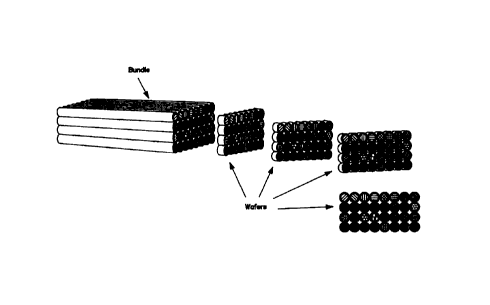
FIGURE 1 illustrates the introduction of reagents into tubes. The figure shows
the introduction of four reagents, numbered 1 through 4, into four empty tubes
to produce
four reagent-filled tubes. The reagents are indicated by patterns in the
filled-tube lumen.
The reagents exemplify array members, empty tubes exemplify structural members
and
the filled tubes exemplify bundle members, as those terms are used to describe
the
invention.
FIGURE 2 depicts the assembly of eight reagent-filled tubes, numbered 1
through
8, into a flat ribbon. The ribbon provides an example of intermediate
structures that may
be useful in the invention.
FIGURE 3 depicts the assembly of four ribbons, numbered 1 through 4, into a
bundle in which the relative positions of the tubes remain the same. The
illustrated
bundle is comprised of bundle members {filled tubes), which are comprised of a
structural
member (tube) and an array member (reagent).
FIGURE 4 depicts the production of wafers from a bundle. Four wafers are
shown, each one at a different viewing angle. The wafers comprise an array of
the
reagents. Note that the disposition of the bundle members (filled tubes)
aligns the array
SUBSTITUTE SHEET (RULE 26)
CA 02306970 2000-04-14
WO 99119711 PCT/US98/21860
_g_
members (reagents) so that they form the desired array in the wafers made by
sectioning
the bundle.
FIGURE 5 depicts several shapes and configurations of tubes.
(a) shows four configurations of hexagonal tube with a circular lumen: (9)
shows reagent filling an untreated lumen; (2) shows reagent filling a surface-
treated
lumen; (3) shows reagent coating an untreated lumen which remains largely
open, and
(4) shows reagent coating a surface-treated lumen which remains largely open.
The
thickness of the surface treatment and reagent-binding layers are not to scale
with the
tube or lumen.
(b) shows several different shapes of tubes and configuration of lumen.
The depiction is merely suggestive of the wide variety of tube and lumen
shapes and
combinations thereof useful in the invention.
FIGURE 6 illustrates assembly of wafers into sub-assemblies and modules. The
top of the figure shows a wafer with 400 array members in a 0.2 cm X 0.8 cm,
10 X 40
array. The middle of the figure shows five wafers containing 2,000 array
members in a
1.0 cm X 0.8 cm sub-assembly. The bottom of the figure shows six sub-
assemblies
containing 30 wafers and 12,000 array members in a 2.0 X 2.4 cm module. The
figure
illustrates the build up of a large device from smaller units, which provides
multiple ways
to incorporate a given tube section into a device, and multiple chances to
correct a faulty
array member section in any one wafer or set of wafers.
FIGURE 7 illustrates a device for contacting a wafer with samples and reagents
for analysis. The device is shown from the top in a and from the side in b. It
is shown
from the side in c, joined to a reagent-delivery manifold. 1 is the wafer
module. 2 is a
sample delivery port. 3 is a reagent delivery port. 4 is a reagent exit port.
5 is the flow
channel for sample and reagent, which runs from the sample and reagent entry
ports
directly over the wafer module to the reagent exit port. 6 is three areas for
human and/or
machine readable information on the device. 7 is sample being loaded into the
sample
loading port, covered by a septum (dark rectangle). 8 is a reagent delivery
manifold with
reagent delivery port 9 and reagent removal port 10. O-ring gaskets (black
partial circles)
provide a fluid-tight seal between the device and the manifold. Disposable
"needles" in
9 and 10 puncture the septa of 2 and 4 to isolate the delivery channels of the
manifold
from the device.
The present invention relates generally to methods of making arrays, to
arrays,
to using arrays, to devices for making arrays, and to devices for using
arrays, among
other things. In particular, the invention relates to producing arrays by
sectioning a
SUBSTITUTE SHEET (RULE 26)
CA 02306970 2000-04-14
WO 99/19711 PCT/US98I21860
-10-
bundle comprising array members, to arrays thereby formed, to using these
arrays, to
devices for making arrays by bundling sectioning methods, and to devices for
using the
arrays formed by these methods, among other things.
The following brief preliminary discussion is provided to facilitate
understanding
some aspects of the invention and terms used to discuss them, by way of
reference to
the specific embodiment of Figures 1, 2, 3 and 4. Figure 1 shows four
individual reagents
introduced into four individual tubes to produce four filled tubes. The
reagents, which will
make up the array, are examples of array members. The tubes, which provide a
structure for holding the liquid reagents, are examples of structural members.
The filled
tubes, which will be combined with other filled tube to form a bundle, are
examples of
bundle members. Figure 2 shows the assembly of fibers into ribbons,
illustrating the
formation of an intermediate structure useful for forming bundles. Figure 3
shows the
assembly of ribbons into a bundle, illustrating the formation of a parallel
coherent bundle
in which the tube maintains the same position relative to other tubes
throughout the
illustrated length of the bundle. Figure 4 shows the bundle again and four
wafers
produced by sectioning the bundle. Each wafer comprises the same array of
reagents,
and the figure illustrates the formation of identical arrays (in the wafers)
by wafering a
bundle. The filled tubes align the reagents in the bundle so that the desired
array is
produced when the bundle is wafered. In this regard, the filled tubes
exemplify the use
of bundle members to align the array members. Since, in the figure the array
members
(reagents) are disposed evenly within the illustrated bundle members (filled
tubes), the
bundle members are disposed identically throughout the bundle and the sections
are cut
identically, the array members are arranged identically in all the wafers in
the illustration.
In sum, the Figures illustrate a simple process of the invention for aligning
array members
in a bundle to produce arrays.
The invention, which is discussed in detail below, is not limited in any
aspect~to
the particulars of the embodiments illustratively set out in Figures 1, 2, 3
and 4. Rather,
the invention can be carried out with practically any shapes or sizes of array
members
and materials, and relates generally to any methods, arrays, and devices
involving
sectioning a bundle of aligned array members. General aspects of the invention
in these
and other regards, as well as many other particulars of specific embodiments,
are
described below. However, the discussion herein is necessarily illustrative,
and a true
understanding of the invention will be possible only by consideration of the
disclosure as
a whole from the point of view of those skilled in the arts to which it
pertains.
SUBST>iTUTE SHEET (RULE 2B)
CA 02306970 2000-04-14
WO 99/19711 PCT/CJS98/21860
-11-
ARRAYS
Generally, as to the invention disclosed herein, an array is an arrangement of
array members. Often it is convenient to define an arrangement by positions of
array
members relative to one another in an array. A given arrangement may be
defined in this
way by the relative positions of some but not necessarily all of the array
members in an
array. In certain preferred embodiments, array members are in fixed positions
in an
arrangement.
In one general aspect, the invention is useful to produce replicate arrays all
having
the same arrangement of array members. In certain preferred embodiments of the
invention, array members are disposed in the same arrangement relative to one
another
in all replicates of a given array. In certain highly preferred embodiments of
the invention,
the array members have the same fixed positions in all replicates of a given
array. In
other embodiments of the invention, some or all array elements in individual
replicates
vary in positions relative to one another. Where the arrangement varies
between
replicates, in preferred embodiments of the invention, the array members can
be
identified by other information.
ARRAY MEMBERS
Array members may be anything to be arrayed or arrayed. For instance, to give
just a few examples, array members may be atoms, molecules, thin films,
ceramics,
glasses, metals, polymers, compounds, compositions, gels, mixtures,
combinations of the
foregoing and just about any other composition of matter. Preferred are those
that have
or are useful to identify or determine in other substances physical,
electrical, magnetic,
electromagnetic, chemical, biochemical, biological and other properties of
interest.
Examples of preferred embodiments in this regard include those that: bind
analytes,
absorb light, fluorescence, quench fluorescence, phosphoresce, those that are
chemiluminescent, electroluminescent, sonoluminescent, piezoelectric, those
that are
polymers, metals, alloys, ceramics, organic compounds, inorganic compounds,
biomolecules and biomaterials of interest, such as those to be screened for
desired
properties or those to be used as screening agents for properties of other
substances,
and combinations of any of the foregoing. Particularly preferred embodiments
in this
regard include polypeptides, including partial or complete proteins and
peptides,
polynucleotides, such as DNAs and RNAs, including relatively long
polynucleotides and
oligonucleotides, compounds that bind to polynucleotides sequence-
specifically, such as
peptide nucleotide acids and DNA sequence-specific polyamides,
polysaccharides,
ligands, ligand-binding biomolecules, molecules of pharmaceutical interest,
chelating
agents or those that bind to chelating agent-derivatives, fractions of cells
or tissues, parts
SUBSTITUTE SHEET (RULE 26)
CA 02306970 2000-04-14
WO 99/19711 PCC/US98I21860
-12-
of cells or tissues, whole cells, whole living cells, derivatives and modified
forms of the
foregoing, and mixtures of any of the foregoing, to name just a few. In fact,
arrays of the
invention are not limited to any particular type of array member, and the
foregoing
examples, as well as the other examples set forth elsewhere herein are
necessarily
merely illustrative.
Particularly preferred in certain embodiments of the invention relating to
binding
assays, as described in greater detail herein below, are binding reagents,
such as, but
not limited to, DNAs, RNAs and other pofynucleotides, polynucleotide-
derivatives, such
as PNAs and other polymeric compounds, such as certain polyamides, that bind
to
polynucleotides in a sequence-specific manner, antibodies and antibody-derived
binding
reagents, antigens, ligands, receptor polypeptides and derivatives thereof,
aptamers, that
bind specifically to cognate compounds or to cognate groups of compounds, such
as
DNA or RNA aptamers and polypeptide aptamers, to name just a few examples in
this
regard.
In general, array members may be any shape. For instance, an array member
may be round, oval, ellipsoidal, triangular, square, rectangular, trapezoidal,
pentagonal,
hexagonal, octagonal, other regular or irregular polygon or any other regular
or irregular
shape. In preferred embodiments, the array members are uniformly shaped
throughout
the bundle. In other preferred embodiments the array members are homogeneous
throughout the bundle. In particularly preferred embodiments the array members
are
both homogeneous and uniformly shaped throughout the bundle. For example, the
array
members in Figure 4 are both homogeneous and uniformly shaped throughout the
bundle. The same would be true for tubes having the cross-section shown in
Figure 5.
In some embodiments, such as those in which an array member itself serves as
the structural member (see below for discussion of structural members) the
array
member may be shaped independently of a separate structural member. In other
embodiments, an array member may be shaped by a structural member. Two
illustrative
specific embodiments in this regard are depicted in Figure 5. The array
members in the
figure are distinct from the structural members. In 5(a){1 ) and 5(a)(2) the
array members
are circular discs. In 5(a)(3) and 5(a)(4) the array members are annular with
circular
inner and outer perimeters. in all four examples the array members are
disposed within
a support having a circular inner perimeter and a hexagonal outer perimeter.
An array member may be formed independently of structural members. In
addition, an array member may be formed within or on a structural member.
Thus, for
instance, to give but one particular example, an oligonucleotide array member
may be
synthesized, purified and characterized first and then loaded into a
structural member,
as depicted for the reagents in Figure 1. An aligonucleotide array member also
can be
SU9STiTUTE SHEET (RULE 25)
CA 02306970 2000-04-14
WO 99/19711 PCT/US98I21860
-13-
synthesized directly in a structural member. For instance, solid phase
oligonucleotide
synthesis can be carried out inside glass structural members to produce a
bundle
member comprising the glass structural member and an oligonucleotide array
member
attached inside the structural member. To mention just one other example in
this regard,
peptide array members also may be similarly synthesized on a structural
member. In
addition, array members can be attached to structural members in a precursor
form and
altered into fnal form after attachment.
Array members, such as those discussed, often cannot be formed into stable
shapes for alignment and incorporation into bundles. Furthermore, many array
members
including many of the array members discussed above are useful only in small
amount,
and typically they are manipulated only in solution. It is desirable to
provide these array
members in a solution, suspension or mixture that can be solidified so that
they can be
formed into shapes for alignment and incorporation into bundles. This is
particularly
desirable when solid wafers are being produced and only the exposed surface of
array
members will be useful in the array. Thus, for instance, binding reagents,
such as those
discussed immediately above, can be dispersed in a gel precursor, such as, for
instance,
a solution of polyacrylamide and bis-acrylamide, introduced into a support,
such as a tube
and fixed therein by polymerizing the gel. Since pofyacrylamide commonly is
introduced
into and polymerized in long narrow bore capillary electrophoresis columns
(see below)
, and it is compatible with polynucleotides and polypeptides, it provides an
apt example
in this regard. A wide variety of other materials that can be gelled,
polymerized or
solidified can be useful in the invention in this regard.
Array members can have a wide variety of sizes and spacing, including but not
limited to the following.
In preferred embodiments of the invention, for instance, there can be 10-100,
50-
250, 200-800, 500-1,000, 750-2,500, 2,000-4,000, 2,500-7,500, 5,000-10,000,
7,500-
15,000, 10,000-50,000, 25,000-75,000, 50,000-150,000, 100,000-300,000, 250,000-
750,000, 500,000-1,500,000, 1,000,000-3,000,000, 2,500,000-7,500,000,
5,000,000-
15,000,000 array members in an array.
Particularly preferred are 100-1,000, 1,000-5,000, 5,000-10,000, 10,000-
50,000,
50,000-100,000, 100,000-500,000, 500,000-1,000,000, 1,000,000-10,000,000 and
more
than 10,000,000 array members in an array. Especially particularly preferred
are less
than 1,000, 1,000-10,000, 10,000-100,000, 100,000-1,000,000 and more than
1,000,000
array members in an array.
In preferred embodiments array members have cross-sectional areas of about
0.0025-0.0075, 0.005-0.015, 0.01-0.03, 0.025-0.075, 0.05-0.15, 0.1-0.3, 0.25-
0.75, 0.5-
1.5, 1.0-3.0, 2.5-7.5, 5.0-15, 10-30, 25-75, 50-150, 100-300, 250-750, 500-
1,500, 1,000-
SUBSTITUTE SHEET (RULE 26)
CA 02306970 2000-04-14
WO 99/19711 PGT/US98/21860
-14-
3,000, 2,500-7,500, 5,000-15,000, 10,000-30,000, 25,000-75,000, 50,000-
150,000,
100,000-300,000, 250,000-750,000, 500,000-1,500,000, 1,000,000-3,000,000,
2,500,000-7,500,000, 5,000,000-15,000,000 and 10,000,000-30,000,000 um2.
Array members can be spaced in arrays to suit a variety of applications.
Preferably in many applications array members are spaced about 0.05-0.15, 0.1-
0.3,
0.25-0.75, 0.5-1.5, 1.0 -3.0, 2.5-7.5, 5.0-15, 10-30, 25-75, 50-150, 100-300,
250-750,
500-1,500, 1,000-3,000, 2,500-7,500 or 5,000-15,000 micrometers apart.
The density of array members in arrays preferably is about 10-100, 50-250, 100
350, 200-400, 150-750, 500-1,000, 750-2,500, 2,000-4,000, 2,500-7,500, 5,000-
10,000,
7,500-15,000, 10,000-50,000, 25,000-75,000, 50,000-150,000, 100,000-300,000,
250,000-750,000, 500,000-1,500,000, 1,000,000-3,000,000, 2,500,000-7,500,000
or
5,000,000-15,000,000 array members per square centimeter of cross sectional
surface
area of the array.
In some preferred embodiments, such as flow through embodiments, the flat
cross sectional surface area of arrays are much different than the total
surface area. In
preferred embodiments in this regard, preferred density of array members in
the arrays
is about 10-100, 50-250, 200-800, 500-1,000, 750-2,500, 2,000-4,000, 2,500-
7,500,
5,000-10,000, 7,500-15,000, 10,000-50,000, 25,000-75,000, 50,000-150,000,
100,000-
300,000, 250,000-750,000, 500,000-1,500,000, 1,000,000-3,000,000, 2,500,000-
7,500,000 or 5,000,000-15,000,000 array members per square centimeter of total
surface
area.
Array members also can be of a variety of depths. In preferred embodiments
array members are 0.1-0.3, 0.25-0.75, 0.5-1.5, 1.0 -3.0, 2.5-7.5, 5.0-15, 10-
30, 25-75, 50-
150, 100-300, 250-750, 500-1,500, 1,000-3,000 or 2,500-7,500 micrometers deep.
STRUCTURAL MEMBERS
Often array members are difficult to manipulate in the manner required for
forming
and using arrays in accordance with the invention. For instance, fluids do not
hold their
shape and cannot be formed into specific shapes. Fluid array members, such as
solutions, thus generally must be put into a container to give them an
appropriate shape
and to align them. Structural member is the term used primarily herein for
structures,
such as containers, that provide support for array members, particularly so
they can be
aligned and assembled into bundles. Structural members can serve other
purposes as
well, such as providing additional support for bundle members or for bundles
(see below),
as alignment members in bundles andlor to facilitate assembly of bundles, as
alignment
members for edge to edge or face to face alignment or stacking of wafers
andlor arrays
SU6STtTUTE SHEET (RULE 25)
CA 02306970 2000-04-14
WO 99/19711 PC'lr/ITS98121860
-15-
or both, providing positional markers in arrays and/or wafers andlor providing
informational elements in wafers and/or arrays, to name just a few.
Structural members can be made of a wide variety of materials, as discussed in
the "Materials" section below.
In general, structural members may be any shape. For instance, an array
member may be round, oval, ellipsoidal, triangular, square, rectangular,
trapezoidal,
pentagonal, hexagonal, octagonal, other regular or irregular polygon or any
other regular
or irregular shape. Structural members that have one or more lumen, such as
tubes, are
particularly useful for aligning array members and incorporating them into
bundles.
Structural members can have no lumen, one lumen, a few lumen, such as 1 to 10
lumen,
or many lumen, such as 11 to 100 or 101 to 200 or 201 to 500 or 500 to 1,000
or more
than 1,000. A very few illustrative embodiments in this regard are set out in
Figure 5(a)
and (b), particularly 5(b). Figure 5(a)(1 ) through 5(a)(4) shows a hexagonal
structural
member with a circular lumen. In 5(a)(1 ) the lumen is filled with an array
member
(exemplified by a reagent). In 5(a)(2) the lumen is coated and filled with an
array
member. In 5(a)(3) the array member is coated on the lumen wall, leaving the
lumen of
the structural member largely open. In 5(a)(4) the inner wall of the lumen is
coated, the
array member is layered on the coating, and the inner portion of the lumen
remains open.
5(b) shows square, triangular, rectangular and circular structural members
with one or
more lumen into which array members can be introduced. As noted above,
practically
any shape can be used for structural members. The particular shape employed,
the
number and size of lumen, the disposition of any coating and of array members
with
respect to a structural member can be adjusted to best suit a given
application and array.
Structural members also may be practically any size, typically dictated by the
desired size of the array members in the array. Thus, in particularly
preferred
embodiments structural members have dimensional properties, such as cross-
sectional
areas, spacings, cross-sectional and total density and depth after wafering
set forth
above and elsewhere herein for array members. In particularly preferred
embodiments,
moreover, structural members have lumen that singly or in groups, provide
array
members with the aforementioned dimensions.
Structural members and array members generally are distinct from one another,
but this need not be the case. Array members can provide their own support
and, if so,
they can be aligned and incorporated into bundles without structural members.
However,
more commonly, array members may be attached to or otherwise associated with
or
loaded onto or into structural members. For instance, the reagents, which
depict array
members in Figure 1 are distinct from the round, hollow ltbers which depict
structural
elements. This is but one particular type of embodiment of the invention,
however. In
SUBSTITUTE SHEET (RULE 26)
CA 02306970 2000-04-14
WO 99/19711 PCT/US98121860
-16-
other particular embodiments an array member may be integral to a structural
element,
such as an array member is dispersed in a structural member. In. other
embodiments of
the invention, an array member itself is a structural member. Combinations of
the
foregoing are also useful in the invention.
BUNDLE MEMBERS
In preferred embodiments of the invention, a plurality of array members or a
plurality of structural members comprising array members are grouped together
to form
a bundle. Each member of the bundle can be referred to as a bundle member. By
way
of example, in certain particular bundle member embodiments, for instance, an
array and
structural member are different andlor an array member itself also is a
structural member
andlor an array member is integral to a structural member. These and other
types of
bundle members may be used alone or in any combination in forming bundles. By
way
of illustration by reference to a specific type of embodiment, for instance,
array members
may be reagents and structural members may be round, hollow fibers, as
depicted in
Figure 1. Bundle members are exemplified thus by the round, hollow fibers
filled with
reagents depicted in Figures 1, 2, 3 and 4.
BUNDLES
In accordance with a preferred embodiment of the invention, arrays are formed
by sectioning a plurality of aligned array members or structural members
associated with
an-ay members. in particularly preferred embodiments, the array members are
aligned
in a bundle. In certain very particularly preferred embodiments of the
invention, the array
members are coherently aligned in the bundle. Coherently aligned means, in
this regard,
that the array members are aligned in the bundle so that they can be
identified and
interrogated in arrays produced by sectioning the bundle. In particularly
preferred
embodiments in this regard, coherent means that array members are aligned in
the same
relative position with respect to one another in at least the portions of the
bundle from
which arrays are formed. In especially preferred embodiments in this regard,
the
members are aligned parallel with one another in the bundle. However, the
alignment of
array members in a bundle need not be parallel; many other arrangements can be
used
that provide for ready identification of array members in the array after
sectioning.
A bundle may comprise both array members and other components. Other
components include structural members, as discussed above, material for
binding array
members or structural members together and material for altering the
properties of
structural members or array members, such as light-reflecting or light-
absorbing
properties. A bundle also may comprise alignment members for aligning sections
with
one another, such as for horizontal or vertical alignment or stacking
sections, or for
SU6STIlTUTE SHEET tRULE 26)
CA 02306970 2000-04-14
WO 99/19711 PCT/US98/21860
-17-
mounting sections in a support or other type of device. Other components may
be
configured the same as, similar to or much different from the array members in
the
bundle. Bundle members may be assembled into bundles in final form or in an
intermediate form. If the bundle members are in intermediate form, the bundle
may be
processed to provide bundle members in their final form for wafering.
Processing the
bundle in this regard preferably employs methods that preserve desired
properties of
array members in the array. One illustrative example in this regard is
provided by a
method for making arrays with nanochannel structural members in accordance
with the
invention.
WAFERS
Wafers, in accordance with the invention, comprise arrays and are produced
from
bundles. Generally, wafers are produced by cutting across a bundle, by which
is
generally meant sectioning a bundle at an angle to axis of alignment of the
bundle
members. In preferred embodiments, a bundle is sectioned so that all array
members
are disposed in the same way in the resulting wafers. Put another way, in
preferred
embodiments a bundle is sectional so that the arrays are the same in each of
the
resulting wafers. In particularly preferred embodiments in this regard the
array members
are in the same positions in the assays in each of the resulting wafers.
In a highly particularly preferred embodiment wafers are made by sectioning a
bundle perpendicular to the axis of bundle member and array member alignment,
much
as illustrated in Figure 4. In other preferred embodiments wafers are produced
by
sectioning a bundle at oblique or acute angles to the axis of alignment.
Sectioning at an
angle may be preferred where it is desirable to expose a larger surface area
of array
elements in the surface of the wafer. For instance, cutting the bundle in
Figure 4 at such
angles would expose ovoid sections of each array member on the wafer surface,
which
would provide greater surface areas than the circular sections shown in the
figure.
Likewise, cutting a bundle at an acute or oblique angle to the alignment axis
provides a
larger wafer than cutting perpendicular to the alignment axis.
Wafers may be formed with planar faces, as illustrated in Figure 4, and as
discussed immediately above, or with any of a very wide variety of other
shapes. For
instance, wafers may be made with a v-shaped surface, a rippled surface, a
grooved
surface, a deeply trenched surface, and the like. In fact, wafers can be made
in
accordance with the invention with just about any shape, particularly those
that can be
made readily by shaping a cutting instrument and controlling its movement as
it sections
a bundle.
SUBSTtTUTE SHEET (RULE 26)
CA 02306970 2000-04-14
WO 99/19711 PCTIUS98/21860
-18-
The faces of a wafer may be the same or different. Wafers with the same front
and back faces can be made by using the same cut to section a bundle on both
sides of
the wafer. Wafer faces can be made different by using different cuts to
section a bundle
on each side of the wafer.
In much the same ways as described above for wafer faces, the wafer sides can
be made symmetrically or asymmetrically in an equally wide variety of shapes,
by, for
instance, processing the sides of the bundle prior to wafering.
Wafers of any given shape, moreover, can be further processed to alter
features
of the faces or the sides or both.
Cutting, milling, drilling, forming, abrading, smoothing, pulling, extruding
and other
forming techniques well known to the fabrication arts, particularly techniques
used to
shape, form and ftnish metal, ceramic, glass and plastic can be employed in
the present
invention to produce and shape wafers to suit a given application.
MATERIALS
Virtually any material can be used for making arrays in accordance with the
invention. The choice of materials for a given array will depend on details of
the array
members, how they will be incorporated or affixed in bundles, how the bundles
will be
assembled and processed, how the bundles will be sectioned for wafer
production, how
the wafers will be processed and how the arrays are to be used, to mention
just a few
considerations. Generally, where an array member is not itself the sole
structural
member of a bundle member or a bundle, there is greater freedom to choose
material to
be used for a structural member.
In general, materials suitable for use in the invention include any materials
that
can be shaped into desired form for structural and bundle members. Generally,
materials
that are relatively easy to form are prefer-ed. Particularly preferred are
materials that can
be shaped to very high precision and very small feature sizes. Thus,
particularly
preferred materials possess the ability to form a desired configuration with
specified
dimensions and properties, including, but not limited to desired thickness and
density
(including having channels); the ability to load it with array members; and
tolerance for
various treatments including for instance, those associated with producing
bundles and
wafers and those associated with use of arrays. Among such particularly
preferred
materials are those that can be formed into long, narrow bore members. for
example
hollow fibers, that can hold array members and can be joined in bundles in
accordance
with the invention herein disclosed. Also preferred are materials that can be
wafered
conveniently, with high precision and very small geometries. Among
particularly
preferred materials, as well, are materials that are compatible with array
members. That
SUHST1TUTE SHEET tRULE 26)
CA 02306970 2000-04-14
WO 99/19711 PCT1US98/21860
-19-
is, materials that do not deleteriously interact with or affect array members
during the
process of loading, bundling, wafering, storage, use or any other condition to
which
arrays may be subjected during assembly, production, storage, shipment or use.
Additionally preferred materials are those that are compatible, in much the
same regard,
with downstream process steps and end uses. In one aspect in this regard,
materials
with a high degree of dimensional stability are preferred. In another aspect,
materials
resistant to solvents and materials used in downstream process steps and end
uses are
preferred. In another aspect in this regard, materials are preferred that
facilitate
detection, particularly for analyte detecting andlor determining applications
of the
invention.
Clearly, the invention can be practiced in too many ways to elaborate more
than
a few herein. Those skilled in the pertinent arts, having understood the
invention, by
taking into account such general considerations as those set out above and
others that
may be pertinent, should be able to choose appropriate materials of
practically any sort
that will be effective to carry out the invention in any particular
application and
circumstance. A few illustrative particulars are set out below as further
guidance in this
regard.
Particularly useful materials for making arrays in accordance with the
invention
include glasses, plastics, ceramics and metals. This is particularly the case
for
embodiments in which hollow fibers (of whatever exterior and lumen shape) are
used to
make arrays, because very long hollow fibers are readily fabricated from these
materials
and in many cases are commercially available. Moreover, particularly for glass
and some
plastics, many surface treatments and chemical derivations are well known that
can be
used to bind array members to structural members, for instance, or to bind
structural
members to one another, or to bind bundle members together to form bundles, to
mention just a few. Similarly, many surface treatments and derivations are
known for
these materials that can be used for other aspects of the invention, such as
detection.
Glasses are particularly preferred for the invention. A variety of well known
fabrication techniques can be used to shape a glass into configurations for
use in the
invention. Likewise, a great many available glass formulations, treatments and
chemical
modification techniques readily can be employed in the invention. Thus, to
mention just
a few types of glasses: standard glasses, functionalized glasses and glass-
ceramics all
may be used in the inventions. Useful information in this regard is provided
in The
Biomedical Engineering Handbook, J.D. Bronzino, ed., CRC Press, 1995,
particularly at
pages 566-580, which is herein incorporated by reference in part pertinent to
using glass
in the invention.
SUBSTITUTE SHEET (RULE 26)
CA 02306970 2000-04-14
WO 99/19711 PCT/US98I21860
-20-
More particularly, long glass hollow tubing is preferred for certain
embodiments
of the invention. Tubing of this type is commercially available in the form of
gas
chromatography ("GC") column tubing, capillary electrophoresis ("CE") column
tubing and
hollow fiber optic tubing. GC column tubing is available off the shelf, in
length of several
meters, with an outer diameter ("OD") of 350 micrometers or less and with
various inner
diameters ("ID") generally in the range of 50 to 200 micrometers for tubing
with an OD
of 350 micrometers. Generally, GC column tubing can be obtained with various
inner wall
coatings designed to facilitate GC analysis. Some of these coatings can be
used
advantageously to increase or decrease interactions of array members with the
inner wall
GC tubing used as a structural member, for instance. Other coatings may be
useful for
immobilization of certain types of array members. GC column tubing is
available in a
variety of glasses, with, as well as without, such coatings. Moreover, the
processes used
to make GC tubing are not limited to the aforementioned dimensions and can be
used to
custom fabricate tubing with other dimensions, including tubing that is meters
or even
hundreds of meters long with much smaller OD and lD.
CE tubing is available with dimensions similar to that of GC and also can be
fabricated in a wide variety of other dimensions. CE tubing is particularly
advantageous
in one regard, since it often is designed to contain a polyacrylamide gel. The
techniques
developed for CE columns for delivering polyacyriamide into CE columns and
then
polymerizing it to form a gel in situ are particularly in certain embodiments
of the present
invention in which an array member is introduced into a structural member in a
solution
that is then solidified in situ.
Hollow glass fiber optic tubing also is available with advantageous dimensions
and
properties. Glass pulling techniques for fiber optic tubing are highly
advanced, and it is
routine to manufacture single tubes several miles long. Although such fibers
typically
have solid cores, similar techniques can be used to produce very long, very
narrow
hollow fibers.
Useful plastics andlor polymers include, among a great many others,
polycarbonate, polyethylene, methylmethacryiate, polypropylene, polyester,
(poiy)tetrafluoroethylene, (poly)vinylidenenedifluoride and the like. Many
other plastics
and polymers that can be used in the invention are well known to those skilled
in the art,
such as those described in, among other well known references, Modern
Plastics,
Encyclopedia '97, Volume 73, Nov. 1996 and The Biomedical Engineering
Handbook,
J.D. Bronzino, ed., CRC Press, 1995 (in which, pages 581-610 are particularly
useful in
this regard), both of which are herein incorporated by reference in their
entirety in parts
pertinent to using plastics andlor polymers in the invention.
SU6ST1TUTE SHEET (RULE 26)
CA 02306970 2000-04-14
WO 99/19711 PCT/US98/21860
-21-
A great variety of plastic fiber and tubing is available for use in the
invention.
Readily available polyethylene ("Intermedic") tubing is available in several
lengths with
an OD less than 500 microns. Hollow plastic fiber optic tubing also is
available,
Moreover, plastic of desired dimensions, such as tubing of particular length,
OD and ID,
generally can be custom fabricated at reasonable cost to just about any size
and
configuration.
Similarly, ceramic and metal tubing for use in the invention can be obtained
commercially in off the shelf dimensions or can be custom fabricated.
Technology developed for manufacturing image pipes can be adapted to and
provides guidance for the assembly of coherent bundles in accordance with the
invention.
Image pipes are bundles of optical fibers that transmit an image from one end
surface to
the other. The optical fibers in the pipe are arranged "coherently," which is
a term of art
meaning that fibers maintain the same position relative to one another in the
cross-
section everywhere along the length of the pipe.
As noted elsewhere herein, optical fibers per se consist of a core and a
cladding,
both solid. Fibers can be made of silicon glass or certain plastics. Fiber of
submicron
diameter can be mass manufactured. Hollow fibers can be manufactured by
similar
techniques either directly or by forming fibers with a core that can be
removed. Some
methods for making fibers, particularly from glass, are set out in Hecht,
UNDERSTANDING FIBER OPTICS, Sams Division of Prentice Hall, Carmel, Indiana
(1987}, which is incorporated herein by reference in its entirety relating to
manufacture,
coating, mating and principles of fiber and fiber optic manufacture and use.
Generally,
as noted elsewhere herein hollow core optical fibers are preferred.
One familiar use of light pipes is in arthroscopic surgical devices to pump an
image from inside the body to the operating physician. The same techniques
used to
assemble individual optical fibers in perfectly parallel arrangement also may
be used to
assemble fibers of other types in this fashion. However, techniques for making
light pipes
that involve pulling arrays of glass tubes down to a narrow bore typically
involve high
temperatures that often are not compatible with array members.
PROCESSING BUNDLES PRIOR TO WAFERING
Some preferred embodiments involve processing a bundle prior to wafering. In
a particularly preferred class of such embodiments bundles are processed prior
to
wafering to alter the dimensions of array members. In embodiments of this
type, bundles
are made of materials that can be pulled (stretched, elongated), preferably
repeatedly,
preferably to form extremely small channels. It also is preferable that
materials allow the
SUBSTITUTE SHEET iiRUILE 26~
CA 02306970 2000-04-14
WO 99119711 PCTIUS98/21860
-22-
bundles to be divided into sections, particularly after pulling and,
preferably, sections from
the same or different bundles joined or fused to one another along their
sides, so that
many bundle members can be pulled in concert. A group of these filled bundle
members
are aligned and affixed in a bundle. The bundle is pulled, without changing
total volumes,
so that the bundle members are greatly elongated and greatly decreased in
cross section.
This process is repeated, combining the same or different bundles after
pulling, to form
bundles of desired geometry. For instance, a circular bundle member 1 cm in
diameter
and 10 centimeters long can be pulled to 100 times its length to form a bundle
member
0.1 centimeters in diameter and 10 meters long. 100 such pulled bundle
members, each
containing a different array member can be aligned in a bundle. This bundle
can be
divided into 100 equal bundles each 10 centimeters long. When pulled to 100
times its
length each of these 10 centimeter long bundles will form a bundle 10 meters
long in
which each bundle member is 100 microns in diameter. 100 such bundles each
containing different array members can be joined into a single bundle
containing 10.000
different array members in 10,000 different bundle members each about 100
microns in
diameter. Sectioning all 10 meters of this bundle into wafers 150 microns
thick, with 50
microns waste between wafers, can provide 50,000 wafers about 150 microns
thick, each
containing 10,000 array members in 10,000 bundle members 100 microns in
diameter.
Forming and sectioning all 100 of the equal bundles in the same way can
provide a total
of 5,000,000 wafers. Thus, 10,000 bundle members originally 10 centimeters
long and
1 centimeter in diameter can provide 5,000,000 wafers each containing
replicate 10,000
member arrays.
One embodiment in this regard, particularly useful to make arrays with lumen,
such as flow through arrays, utilizes two materials. One is resistant to and
the other is
degraded by a process herein referred to as an excavating process. Array
members are
immobilized on the lumen wall of support members formed of the resistant
material. The
lumen then are filled with the material that is degraded by the excavation
treatment.
Once inside the lumen the material is solidified. Pulling, sectioning and
wafering is
carried out as described immediately above, with the same effect. Wafers
produced from
the pulled bundles then are subjected to the excavating process, which
degrades the fill
material and reopens the lumen, now of much reduced cross-section. A technique
of this
types is used to make nanochannel glass wafers that can be used in flow-
through
biochips, such as those being developed by Gene Logic. However, in that case,
the
nanochannel glass is manufactured first and then patterned with
oligonucleotide probes.
The glass manufacturing process involves treating glass wafers with very
strong acid to
remove acid-sensitive glass core material and form nanochannels. The acid is
not
compatible with many array members, such as oligonucleotides. Excavating
treatments
SUBSTITUTE SHEET tiRUL.E 25)
CA 02306970 2000-04-14
WO 99/19711 PCT/US98/21860
-23-
in these embodiments, therefore, preferably are compatible with the array
members and
intended uses of the arrays. Excavating processes that can be useful in this
regard
include light mediated degradation of light-degradable plastic.
$EC,;TIONING BUNDLES TO FORM WAFERS
Wafers can be cut from bundles using any of a wide variety of methods, in a
very
wide variety of ways. As noted elsewhere herein, for example, the attack of
the cut can
be perpendicular to the bundle or it can be at a different angle. Cuts can be
symmetrical
or asymmetrical, both with respect to the bundle itself andlor with respect to
the two sides
of the wafer. Asymmetrical cuts, particularly of the latter type, are useful,
for instance,
especially when the faces of a wafer are desirably different. Cuts can be
planar (flat) or
they can be other shapes. Particularly preferred in this regard, for example,
in addition
to planar cuts, are cuts that increase or facilitate exposure of array
elements desirable
in an end use, such as saw tooth cuts that deeply corrugate array members
thereby
increasing their exposure. Cuts can be complete in themselves or can be
compounded
with one another to produce more complexly shaped sections, as well. These are
but a
few of the variations possible in this regard.
Many types of cutting methods can be used to section bundles to produce wafers
and arrays in accordance with the invention. A number of parameters generally
should
be considered in choosing the method to use in a given application and
circumstance.
First, the cutting method should be effective for all the materials in the
bundle, including
array members, any structural members and any other components of the bundle
that are
to be sectioned. The cutting method should be compatible with the bundle
components,
particularly the array members and any other components important to further
processing
or using the wafer and the array being produced. Methods that minimize waste
are
particularly preferred. Thus, where mechanical cutting is employed, methods
that
minimize kerf are preferred in this regard. Methods that minimize
contamination are
preferred as well. To produce wafers from open bundles (i.e., bundles with
openings in
cross section) cutting methods that do not foul or close the opening are
preferred.
Generally, preferred cutting methods also minimize environmental stress, such
as heat,
exposing the bundle and wafers to abrasives or to lubricants, solvents,
coolants or the
like, especially stresses that may deleteriously effect array members or
functional aspects
of arrays and/or wafers. The following discussion of more specific cutting
methods
further illustrates this aspect of array production in accordance with the
invention. In
general, methods that can cut with greater precision are more highly preferred
than less
precise methods. In particular, for many applications and embodiments, the
thinner the
SU6STIfTUTE SHEET (RULE 26)
CA 02306970 2000-04-14
WO 99/19711 PCT/US98121860
-24-
sections that can be produced the better. In this regard, low vibration,
positionally stable
cutting methods are preferred.
Mechanical methods for cutting, among other things, glass, plastics, ceramics
and
metals are well known. Such cutting devices that can be used to section
bundles to
produce wafers include knife-edge devices. Microtomes are a notable of the
type of knife
edge device that can be used to section bundles to provide very thin sections.
Microtomes are designed to produce serial thin sections of tissue, typically 1
to 10
micrometers thick. Commercially available microtomes designed for sectioning
fixed
materials are useful in some embodiments of the invention in this regard.
Likewise,
cryostats (microtomes designed to cut frozen material) can be used to cut
bundles in
some embodiments of the invention. Both types of microtomes are particularly
advantageous for sectioning bundles, when they are compatible with the bundle
materials. They provide smooth cuts and surfaces. Generally, microtome cuts do
not
produce discernable contamination across the cut surface. The cuts can be made
without distorting shape. Serial cuts are uniform. Spacing of cuts can be
controlled very
precisely and accurately. The cuts do not produce waste. They do not generate
heat
and they do not require lubricant, solvents or cleaning solutions. They can be
readily
automated to cut through a bundle continuously and to place each wafer in turn
onto a
carrier or other device, as desired.
Ultra high pressure liquid cutting is another useful technique for sectioning
bundles to produce wafers in accordance with the invention. Ultrafast, jet
streams of
liquid, such as those used to cut steel and other metals, provide a clean,
precise,
temperature controlled cut that can be quite useful in some embodiments of the
present
invention. Methods of this type are particularly preferred for cutting glass,
metal and
ceramics, particularly when microtomes cannot be used.
Laser cutting also is a preferred cutting technique in certain embodiments of
the
invention.
Other mechanical cutting devices that may be useful in the invention include
rotary and reciprocating cutting devices, including circular saws, band saws
and wire
saws, to name just a few. Tools of this type can be used in the invention, in
keeping with
the foregoing considerations.
The foregoing list is merely illustrative. Clearly, a great many other
techniques,
well known to those of skill in the pertinent arts, can be used to section
wafers in
accordance with the foregoing requirements.
SU9STtTUTE SHEET (taULE 2B)
CA 02306970 2000-04-14
WO 99/19711 PCT/US98I21860
-25-
ILLUSTRATIVE EXAMPLES RELATING TO ANALTYE ANALYSIS
The following discussion illustrates various aspects of the invention, by
reference
to certain specific embodiments useful to detect and, in some cases quantify,
analytes
in samples. The discussion is merely illustrative and discloses general
features of the
invention solely by way of specific examples. The invention is not limited in
any way to
particulars or details of these examples. For instance, the invention is not
limited to
analyte detection or quantification using analyte binding reagents, as is the
discussion in
these examples. Likewise, the invention is not limited to the particular
assays or array
formats discussed below. Rather the examples merely exemplify a few preferred
embodiments of the invention and thereby illustrate aspects of its more
general features.
Detecting and quantitating substances of various sorts in a wide variety of
samples are important components of many economically important activities.
For
instance determining analytes, such as molecular, macromolecuiar and cellular
analytes
is important in biological, chemical, veterinary, clinical, forensic,
agricultural, food,
environmental, consumer products, process stream, quality control, military-
related and
other types of samples. Arrays, array-based devices, and array-related methods
and
apparatuses can be used for analysis of analytes in all of these types of
samples, among
others. Analyte determining arrays can be used in this regard for, to name
just a few
examples, clinical and veterinary diagnostic analyte analysis, forensic
analysis, food
quality monitoring, agricultural monitoring, environmental monitoring,
monitoring of
microbial agents, chemical and biological warfare agent monitoring, and
process control
monitoring. The following discussion illustrates the use of the invention in
regard to
specific embodiments of analyte-determining arrays.
NOMEN~:LATURE IN THE FOLLOWING DISCUSSIC,~N
A variety of terms are used in the following discussion in ways specifically
relating
to the exemplified analyte-determining embodiments of the invention. The
following
discussion provides illustrative explanations of some of the terms, as an aid
to
understanding the discussion and, thereby, the invention. However, the brief
discussion
immediately below does not provide exhaustive definitions, and it is not
intended to
circumscribe limitations of the invention, which can only be understood from
careful
consideration of the disclosure as a whole in light of related and ancillary
knowledge in
the arts to which it pertains.
sample Samples suitable for analysis in the present invention include any
sample that can be brought into contact with assays in a chip for effective
detection or
quantification of an analyte. Preferred samples are homogeneous liquid
samples.
SUBSTITUTE SHEET (RULE 26)
CA 02306970 2000-04-14
WO 99/19711 PCTNS98/21860
-26-
Included are biological fluids such as blood, serum, urine, saliva, spinal
fluid, tears,
lymph, bile, peritoneal, and wound fluids. Also included are homogenized
biological
samples such as homogenized mucous and homogenized bowel samples, as well as
homogenized biopsy samples. Preferred samples include the aforementioned
biological
fluids, of which blood, serum, urine and salvia are particularly preferred.
analvte In the following discussion, any molecule, compound substance,
organism or other thing that is to be detected or quantified is referred to as
an analyte.
gig In the following discussion, a reagent that binds to and is useful for
detecting, quantifying or analyzing one or more analytes is referred to as an
analyte
binding reagent ("ABR"). Generally, an ABR is any entity that binds to and can
be used
to detect the presence or determine the amount of an analyte. An ABR and the
analyte(s) it binds are referred to as cognates. In some preferred embodiments
the ABRs
bind their cognate analytes very tightly and with great specificity. In other
preferred
embodiments, ABRs bind their cognate analytes much less tightly and with much
less
specificity. Such lower affinity and specificity ABRs are particularly useful
in arrays that
implement nose-like sensing paradigms. Analytes can be detected and quantified
by
binding to one or to more than one ABR.
molecule. compound. etc. It will be appreciated that any atom, molecule,
complex of molecules, mixture of molecules or molecular complexes, molecular
aggregates, macromolecular or other complexes, aggregates, combinations of the
foregoing or any other assemblage of matter can be used in accordance with the
present
invention if it is useful to the determination of any other assemblage of
matter (as
illustrated by the foregoing illustrative listing) and it can be incorporated
into the devices
of the invention or used in the methods and apparatus of the invention herein
described.
The terms molecule and compound and related terms generally are used herein to
refer
to any of these.
imp As used below, chip means the same as wafer, and as unit, unit surface
and dice.
elemenf Usually the smallest feature on a chip is referred to as an element.
Most
often it constitutes a defined area that contains a particular analyte binding
reagent. The
signal from an element may be obtained by sampling and calculation. Thus, for
instance,
a laser (or other sensing element) for reading an array can be smaller than
the array
elements, in which case the smallest signal-generating area is defined by the
laser, not
the an-ay.
assay The part or parts of a chip relating to a given assay or test is
referred
to as an assay or assay areas. An assay may comprise one or more elements,
which
may be grouped or distributed in an array. For instance, an assay may comprise
a
SU9STtTUTE SHEET tRULE 26)
CA 02306970 2000-04-14
WO 99/19711 PCT/US98/21860
-27-
graded concentration of an ABR to provide a quantitative curve of analyte
binding. An
assay also may comprise negative and positive controls.
autoanalvser An instrument for automatically processing sample test matrixes,
generally comprising (1 ) a mechanism to transport carriers through the
instrument, (2)
a microprocessor controlled liquid delivery system that delivers appropriate
reagents to
the test matrix according to its type, (3) a system for digitizing all the
assay results within
each element in the matrix, and (4) a computerized analysis system to
determine the
results of each assay, to report the results, and to bill for the requested
tests.
GENERAL CONSIDERATIONS FOR ANALYTE ANALYSES USING ARRAYS
The nature of the ABRs, the analytes and the samples) in which the analytes
are
to be determined largely will determine the analytic chemistries that are used
in a given
type of assay of the invention. Those of skill will appreciate from the
present disclosure
how to adapt particular assay systems for use in the present invention. Many
analytic
chemistries have been described and are well known to those of skill in the
art that can
be usefully employed in accordance with the present invention. These are
described
broadly in, for instance, BIOSENSORS, AN INTRODUCTION, Wiley and Teubner,
Chichester and Stuttgart (1996), HANDBOOK OF BIOSENSORS AND ELECTRONIC
NOSES, MEDICINE, FOOD, AND THE ENVIRONMENT, Erika Kress-Rogers, ed., CRC
Press, Boca Raton (1997) and IMMUNOCHEMICAL ASSAYS AND BIOSENSOR
TECHNOLOGY FOR THE 1990S, Nakamura et al., eds., American Society for
Microbiology, Washington, D.C. (1992), each of which is herein incorporated by
reference
in its entirety in parts pertinent to analyte analysis procedures and
chemistries.
Numerous other publications, such as those cited in the forgoing references,
set out
assay procedures in much greater detail, and are well known to those of skill
in art.
The invention provides several features that will be found advantageous in
most,
or all, types of assays. First, the invention provides a method to analyse
many different
analytes in a sample all-at-once. As set forth above, the method utilizes very
small
amounts of ABR to analyse a sample. In the most highly preferred embodiments,
very
small amounts of sample are used. And where reagents are employed, the most
highly
preferred embodiments of the invention use very small amounts of these
reagents as
well.
Similar considerations apply to the sample.
It will be convenient in many cases to employ an autoanalyser to carry out
assays.
An alternative to liquid or gas reagents delivered by an autoanalyser may be
preferred in low use and/or remote environments. In these situations
development
reagents may be provided as part of the platform which will incorporate a
device for
SUBSTITUTE SHEET (RULE 2B)
CA 02306970 2000-04-14
WO 99/19'711 PCT/US98/21860
_28_
controlling delivery of the reagents to the assays effective for properly
developing results.
In a preferred embodiment of this type the reagents are in a gel in a geometry
that
provides reagent assay contact effective for proper development when the gel
is extruded
unidirectionally across the assays following appropriate exposure to sample.
It will be
appreciated by analogy that the operation of this embodiment of the invention
is akin to
the self-developing films that have been marketed by Kodak and Polaroid, among
others,
although the analogy should not be taken too literally.
STANDARDIZATION
It will be appreciated that there may be differences between the assays in an
array. Therefore, each assay in an array may be designed to perform well under
certain
specified conditions to be employed. For instance, the assays in a given array
might all
desirably be designed to work well with a given autoanalyzer of limited
flexibility and
narrow dynamic range of detection. There are many ways to achieve desirable
operative
similarity of array assays in accordance with the invention, a few of which
are described
below.
The amount of ABR can be adjusted for each assay to work well within the
available dynamic range. In addition, the amount of a detecting reagent or the
amount
of label in the detecting reagent may be adjusted. For instance, in a sandwich
antibody
assay, the amount of frst antibody immobilized on the surface may be varied
for each
assay to work well with the expected sample in the available protocols and
detection
regimes of the analyzer. The amount of second antibody that binds to the
antigen also
can be controlled, by its concentration in the second antibody mix. Also, the
degree of
labeling of a detection reagent, such as a fluorescent tag or biotin affinity
label on a
secondary antibody, can be adjusted to help insure that the signal from each
assay is
within the working range of the analyze. For example, by reference to sandwich
assays
using biotinylation, since each first antibody may be separately immobilized,
each second
antibody can be separately biotinylated, and many assays can be tested
simultaneously
in a given autoanalyser protocol. It will almost always be possible to adjust
the
parameters of any particular assay to a standard protocol.
ILLUSTRATIVE ANALYTE ASSAY METHODS
The invention is useful for, among many other things, carrying out any assay
predicated on binding of one member of a binding to the other, such as binding
of an
analyte binding reagent and cognate analyte. Numerous assays have been
described
and are well known to those of skill in the art that can be usefully employed
in accordance
with the present invention. Many such techniques are set out in some detail
in, for
SU85TiTUTE SHEET (RULE 28)
CA 02306970 2000-04-14
WO 99/19711 PCT/US98121860
-29-
instance, BIOSENSORS, AN INTRODUCTION, Wiley and Teubner, Chichester and
Stuttgart (1996), HANDBOOK OF BIOSENSORS AND Et.ECTRONIC NOSES,
MEDICINE, FOOD, AND THE ENVIRONMENT, Erika Kress-Rogers, ed., CRC Press,
Boca Raton (1997} and IMMUNOCHEMICAL ASSAYS AND BIOSENSOR
TECHNOLOGY FOR THE 1990s, Nakamura et al., eds., American Society for
Microbiology, Washington, D.C. (1992), each of which is herein incorporated by
reference
in its entirety in parts pertinent to assay methods.
In certain preferred embodiments of the invention, immunological reagents are
used, particularly antibody-derived reagents. In other preferred embodiments,
oligonucleotide and/or PNA reagents are used. Other preferred embodiments
relate to
organic affinity reagents (ABRs), such as polyamides that can bind DNAs
sequence-
specifically. Still other preferred embodiments relate to random "sequence"
polymers,
such as random sequence DNAs, screened for analyte-binding ability and then
used as
ABRs.
Some preferred embodiments of the invention relate to high affinity and
specificity
ABRs, while other preferred embodiments relate to lower affinity and Power
specificity
ABRs. Particularly preferred regarding low affinity and/or low specificity
ABRs are
embodiments of the invention in which analytes are determined by patterns of
binding to
sets of ABRs. Still further preferred embodiments relate in this regard to
combinations
of ABRs with differing specificity, affinity and avidity for their cognate
analytes.
Particularly preferred embodiments use information from a variety of such ABRs
to
determine an analyte.
Illustrative analyte assay methods for use in the invention are described
below.
However, the illustrative methods are only a very few among many well known
assay
paradigms that can be practiced in the invention.
Sandwich assays
In a highly preferred embodiment, sandwich assays are used in the invention.
In
certain highly preferred embodiments in this regard, first antibodies specific
for cognate
antigens are immobilized in an array, in accordance with methods described
herein
above. The array is exposed to a sample under conditions effective for
antibodies in the
array to bind cognate antigens in the sample. Thereafter, the array is washed
and then
exposed to second antibodies that bind to the cognate antigens under
conditions effective
for the secondary antibodies to form Ab1-cognateAg-Ab2 sandwiches with cognate
antigens bound to first antibodies in the array. The formation of the
sandwiches then is
detected, thus detecting the presence of the cognate antigens in the sample.
SUBSTITUTE SHEET (RULE 26~
CA 02306970 2000-04-14
W O 99/19711 PCT/US98/21860
-30-
Detection can be qualitative or quantitative. Generally, the second antibodies
in
sandwich assays are detected independently of the first antibodies. Thus, the
first
antibodies might be mouse monoclonals and the second antibodies might be goat
polyclonals. More conveniently, first and second antibodies both may be mouse
monoclonal, but all the second antibodies will have been covalently bonded to
a
detectable label, such as a fluorescent label. Other labels, of which many are
know to
those of skill in the art, can be used. Non-diffusing labels are preferable in
some
situations, where diffusion would preclude accurate localization, for
instance. However,
solution ELISAs also can be used in some embodiments.
Alternatively, second antibodies may be attached to a chemical hook which
subsequently attaches the detectable label. The well known avidin-biotin
system can be
used in this way. For instance, the secondary antibodies can be tagged with
biotin, a
fluorescent label can be attached to avidin, and the presence of cognate
antigens can be
detected by fluorescence of labeled avidin that binds to biotinylated
secondary antibodies
in Ab1-cognateAg-Ab2 sandwiches formed on the array.
Those skilled in the art will appreciate the wide variety of immunoassay
paradigms
and the large number of detectable labels that can be used in much the same
way as
discussed above for sandwich immunoassays and fluorescence or ELISA detection.
A
general description of many such techniques that can be used in accordance
with the
present invention is provided in PRINCIPLES AND PRACTICE OF IMMUNOASSAY, 2nd
ed., Price and Newman, eds. Stockton Press, New York (1997), which is
incorporated
herein by reference in its entirety.
Hybridization assays
Also particularly useful in the invention are hybridization assays and methods
for
detecting hybridization. Such assays can take a wide variety of formats and
are well
known to those of skill in the art. Particularly preferred for use in
accordance with the
present invention are assays that work well in a solid-phase format in which a
capture
probe is immobilized on a solid phase, such as a surface, and localizes
specific
hybridization thereto. A number of formats, assay parameters to consider and
detectors
for chip-based hybridization assays are discussed by Titball and Squirrell in
Probes for
Nucleic Acids and Biosensors, Chapter 4 in HANDBOOK OF BIOSENSORS AND
ELECTRONIC NOSES, MEDICINE, FOOD, AND THE ENVIRONMENT, Erika Kress-
Rogers, ed., CRC Press, Boca Raton (1997), which is incorporated by reference
herein
in its entirety. Several formats for hybridization assays are illustratively
discussed below;
but, many other approaches also can be employed in accordance with the
invention.
SUBSTITUTE SHEET {RULE 26)
CA 02306970 2000-04-14
WO 99/19711 PCTNS98I21860
-31-
One approach to hybridization assays is direct detection of duplex formation.
Several methods for so-doing are well known to those of skill in the art.
Further, several
such methods have been implemented in microchips by companies such as
Affymetrix
and Hyseq. In such approaches polynucleotides in the sample are labeled and
their
hybridization to the probe polynucleotides (or PNAs) on the chip are detected
directly.
The labels generally are fluorescent in common implementations of this
approach; but,
many other types of label can be used, as discussed elsewhere herein.
Another approach to such methods is based on primer elongation, exemplified by
the following method for simultaneous analysis of a plurality of
polynucleotides in a
sample, which comprises the steps of: {A) providing a surface having
immobilized in a
predetermined pattern thereon a plurality of first oligonucleotide probes
stably
hybridizable specifically to one or more polynucleotides, wherein the first
oligonucleotide
probes provide 3' hydroxyl groups for elongation, and wherein each position in
the
predetermined pattern exclusively contains a first oligonucleotide probe or
mixture of
probes specific for a polynucleotide or mixture of polynucleotides of the
plurality of
polynucleotides; (B) contacting the surface with a sample under conditions
effective to
hybridize polynucleotides in the sample specifically to the first
oligonucleotide probes or
mixture of probes immobilized on the surface; (C) removing from the surface
components of the sample other than polynucleotides specifically hybridized to
the
immobilized first oligonucleotide probes on the surface; (D) contacting the
surface with
a solution comprising a polymerase for primer extension and a detestably
labeled
poiymerase substrate under conditions effective to extend hybrids formed by
the probes
and polynucleotides of the sample, thereby detestably labeling the hybrids
immobilized
on the surface; (E) removing from the surface the components of the solution
other than
the labeled hybrids immobilized on the surface; and (F) determining the
detectable label
in each position of the pattern on the surface, thereby determining the
polynucleotides
in sample.
In certain preferred methods of this type the detectable label is a
fluorescent label.
In other preferred embodiments other types of labels are employed. Also
preferred are
mass tags for mass spectral detection and analysis. Also preferred in certain
embodiments of this aspect of the invention are methods wherein the polymerase
is a
DNA polymerase and one, two, three or all four of the deoxyribonucleotide
triphosphates
are detestably labeled with a fluorescent label. In other preferred
embodiments in this
regard the polymerase is a reverse transcriptase and one, two, three or all
four of the
deoxyribonucleotide triphosphates are detestably labeled. In certain preferred
embodiments in both regards, fluorescent labels are preferred. In another
regard, certain
preferred embodiments are those in which the Tm or Td of duplexes formed by
SUBST>TUTE SHEET (RULE 2B)
CA 02306970 2000-04-14
WO 99/19711 PCTIUS98I21860
-32-
hybridization of sample polynucleotides to immobilized probes are within 1, 2,
3, 4, 5 or
degrees centigrade of one another. Particularly preferred are those in which
the
duplexes are within 1, 2 or 3 degrees centigrade under the conditions used for
hybridization.
5 Also useful in the invention are methods for simultaneous analysis of a
plurality
of polynucleotides in a sample, comprising the steps of: (A) providing a
surface having
immobilized in a predetermined pattern thereon a plurality of first
oligonucleotide probes
stably hybridizable specifcally to the polynucleotides, wherein the first
oligonucleotide
probes provide 3' hydroxyl groups, and wherein each position in the
predetermined
10 pattern exclusively contains a first oligonucleotide probe or mixture of
probes specific for
a polynucleotide of the plurality of polynucleotides; (B) contacting the
surface with a
sample under conditions effective to hybridize polynucleotides in the sample
specifically
to the first oligonucleotide probes immobilized on the surface; (C) separating
from the
surface components of the sample other than polynucleotides specifically
hybridized to
the immobilized first oiigonucleotide probes on the surface; (D) contacting
the surface
with a plurality of detectably labeled and ligateable second oligonucieotide
probes stably
hybridizable specifically to the polynucleotides, wherein the second and the
first
oligonucleotide probes are ligateably adjacent when hybridized to a
polynucleotide from
the samples; (E) separating from the surface, components of the sample other
than
second oligonucleotide probes hybridized to the polynucleotides hybridized to
the
immobilized first oligonucleotide probes immobilized on the surface; (F)
contacting the
surtace with a ligase for ligating the ligateabiy adjacent first and second
oligonucleotide
probes hybridized to the polynucleotides under conditions effective for
ligating the first
and second oligonucleotide probes; (G) separating from the surface detectable
label
other than detectable label in second oligonucleotide probes ligated to the
first
oligonucleotide probes immobilized on the surface; and (H) determining the
detectable
label in each position of the pattern on the surface, thereby determining the
polynucieotides in sample.
In certain preferred methods of this type, step (G) additionally comprises
melting
the polynucleotides hybridized to the first and second oligonucleotide probes,
whereby
detectably labeled second oligonucleotide probes ligated to first
oligonucleotide probes
remain bound to the surface via the first oligonucieotide probes immobilized
on the
surface in the predetermined pattern, and the other polynucleotides are
removed.
In still another approach to hybridization assays, the immobilized probe
contains
two labels that interact through an energy transfer mechanism that is affected
by duplex
formation. The energy transfer is detectably altered by probe-target binding
in a way that
enables analyte detection and determination. For instance, the two label can
exchange
SU9ST1TUTE SHEET (RULE 26)
CA 02306970 2000-04-14
WO 99/19711 PCT/US98I21860
-33-
energy by Forster energy transfer. Forster energy transfer efficiency is
proportional to
the inverse sixth power of the distance between the two labels. Accordingly,
it is very
sensitive to their proximity. If duplex formation moves the labels even
slightly apart
energy transfer between them will decline dramatically. The effect is well
known to those
of skill in the art, and it has been used to measure the relative motion of
different parts
of various molecules, such as polynucleotides and proteins. Its application in
accordance
with the present invention can proceed using much the same kinds of
techniques,
adapted to the solid phase array.
DETECTION
A wide variety of detection techniques may be employed in the invention for
reading-out analyte determinations on a chip. The detection techniques,
moreover, may
rely on any of a wide variety of detectable labels. Such detection techniques
and
detectable labels are well know and are described in numerous primary
publications,
technical manuals, laboratory handbooks and textbooks, to name a few. These
detection
technologies are described in such publications both generally and with
respect to
specific types of assays and assay procedures. In general, such techniques can
be
employed in the present invention, particularly those that have already been
adapted to
detection of binding to genechips and other types of solid-state arrays. Such
techniques
are described in, for instance, BIOSENSORS, AN INTRODUCTION, Wiley and
Teubner,
Chichester and Stuttgart (1996), HANDBOOK OF BIOSENSORS AND ELECTRONIC
NOSES, MEDICINE, FOOD, AND THE ENVIRONMENT, Erika Kress-Rogers, ed., CRC
Press, Boca Raton (1997) and IMMUNOCHEMICAL ASSAYS AND BIOSENSOR
TECHNOLOGY FOR THE 1990S, Nakamura et al., eds., American Society for
Microbiology, Washington, D.C. (1992), each of which is herein incorporated by
reference
in its entirety in parts pertinent to detection.
Generally techniques for detection in accordance with the invention can
determine
both the presence of a detectable label and its position, relative to other
positions in an
array on a chip. Both abilities can be attained by a variety of means. For
instance,
detection may involve acquiring an image of a chip that comprises an image of
the
detectable label in each element andlor assay area, and then, by image
processing,
determining the results for each assay. Such image processing may be
quantitative,
threshold-related or qualitative. Alternatively, the chip may be scanned,
raster fashion,
or quasi-raster fashion, or along a path (ray-tracing mode) so detection is
carried out
discretely for each element andlor assay area. Each element andlor assay area
thus
may be detected one or more times in the same or in different portions, and
the detection
may involve averaging or otherwise processing such repeated samplings. The
sampling
SUBSTITUTE SHEET (RULE 2B)
CA 02306970 2000-04-14
WO 99/19711 PCT/US9$/21$60
-34-
furthermore may involve detection of each element andlor assay area along a
beam line,
such as for an absorption assay, or it may involve stimulation by a beam line
and
detection of an emitted signal, such as fluorescence. In the latter case, the
emitted signal
may be measured over a spot or a wide area. In addition, the entire chip (or
portions
thereof) can be excited en banc and the signal coming from elements and/or
assay areas
then measured individually. Of course, several beams and detectors can be
arranged
to work in parallel in any such detection paradigm. Spatial resolution may be
obtained
by tracking the motion and the position of a scanning beam (or other scanning
means)
as it moves with respect to a chip, by tracking the position of the chip as it
moves with
1D respect to the beam, or by a combination of the two. In addition, alignment
markers
integrated into the chip, sub-assembly, matrix and/or matrix carrier can
provide internal
alignment and registration signals that can be used by the detector and its
associated
hardware and software to correlate elements and assays on a chip with the
detected
signals. Such alignment and registration signals can be incorporated into
chips as
pseudo-analytes at the time the chip is made. Alternatively or in addition,
the markers
can be "etched" or written onto the chip outside the elements and the element-
containing
portion of the assay areas at the time the chips are made. A wide variety of
other
approaches also may be usefully employed in the invention. Suitability of
detection
techniques for use in the invention can be assessed by reference to the
following
parameters.
The detection accuracy should be high. Preferably, the accuracy is within 2-3%
deviation or better about a norm for repeated sampiing of the same test
result.
For clinics! applications, and other real-time applications relatively short
read-out
times are preferred. Thus, for instance, for clinical and other real time
applications read
out times under an hour, preferably less than 15 minutes and especially
preferably less
than 5 or I minute are preferred.
To accommodate differing analyte concentrations detection techniques that have
a wide dynamic range are preferable.
At best, analyte binding to every assay area on a chip can be detected andlor
determined for each sample.
The detector must be able to resolve the elements and assay areas, and it must
be able to detect the signal in such areas that samples for analysis will
provide.
As noted elsewhere herein, they need not be square but can be any shape.
Moreover, also as noted elsewhere herein, size is limited not by intrinsic
aspects of the
methods and systems herein disclosed but by technical considerations and
limitations on
fabrication equipment, materials and techniques. Those of skill readily will
appreciate and
SUBSTITUTE SHEET (RULE 2fi)
CA 02306970 2000-04-14
WO 99/19711 PCT/US98121860
-35-
apply to the invention improved materials and techniques as they become
available.
Such application specifically is contemplated by the present invention.
Many detectors for use in the invention presently are available. Suitable
detectors
range from inexpensive scanners for use with PC's to sophisticated photon
counting
imaging microscopes. As noted above, different detectors will be preferred in
different
embodiments of the invention. Thus, for economical mass production greater
economy
will be desirable. For other applications very high resolution, sensitivity
and dynamic
range may be more important. The few examples below, therefore, are merely
illustrative.
Sophisticated and sensitive apparatus for detection is available that can be
used
for clinical and other applications in which large numbers of samples are
analyzed, or
where equipment expense is not as important as sensitivity, speed and
accuracy. Thus,
for instance, fluorescence detectors of the type used on automated DNA
sequences can
be adapted for use in the present invention, for detection of one, two, three,
four or even
more fluorescent dyes. Likewise, the fluorescence detectors described by
Affymax and
Affymetrics for detecting binding to peptide and oligonucleotide arrays are
readily
adaptable for use in accordance with the present invention. Likewise, many
laser
scanning detectors now used for biochip detection, including laser-ablation
mass
spectroscopy scanning detectors, are readily employed as detectors in
accordance with
the present invention.
Another approach might be taken for mass producing detectors, that also
illustrates some considerations for implementing both simple and more
sophisticated
detection regimes and systems. This approach, illustratively discussed below,
is to use
a scanner to capture the results of assays. A variety of scanners are
commercially
available, largely for digitizing text and drawings for entry in a computer
file associated
with document production. Nonetheless, the devices are well suited to
capturing any
image in digitized, computer readable form.
The devices have in common that they scan an image surface with a laser beam
and measure the light reflected from the surface along the scan path. The scan
line
typically is very thin, 11100 to 1/400 inches in inexpensive scanners. The
full image is
digitized by serially scanning the image surface in the direction
perpendicular to the scan
line. Thus, scanners typically move paper in steps after each line scan to
build up the two
dimensional image of the paper surface. With hand-held scanners the
perpendicular
movement is performed manually. It will be appreciated that the scanning
mechanism
is compact and economical in these devices.
A relatively inexpensive hand-held color scanner can resolve 400 dpi in both
dimensions, i.e., 16,000 pixels per square inch. Resolution is in three colors
with a grey
SUBSTITUTE SHEET (RULE 26)
CA 02306970 2000-04-14
WO 99119711 PCT/US98/21860
-36-
scale range of 256 levels. Consumer devices are available for digitizing 35 mm
color
photographs for manipulation on a PC. A typical full color, 12-bit, 2,000 dpi
device
resolves 4,000,000 12-bit pixels per square inch. More expensive models can
achieve
very much higher resolution. One device has been reported that can resolve
25,000 dpi,
i.e., 625,000,000 pixels per square inch.
EMBEDD)~"D DATA
The detection system can read coded information on the chip in addition to
assay
test results. Many types of information can be coded, in many formats. One
type of
information is positional, such as the alignment and registration information
discussed
elsewhere herein. Such information primarily is useful to allow identification
of elements
and assay areas with the detected binding, so that signals can be matched to
corresponding elements andlor assays. Such information generally can be
imprinted at
the time the chip is manufactured. Another type of information provides
information about
the chip itself - its manufacturing lot, for instance. This information, at
least in part, can
be used to match software to chips so that the results of assays can be
calculated and
accurately reported. Thus, for instance, the information about each element
and assay
area in each lot of chips on a given carrier can be recorded in software. The
software
thus can contain the identity. location, standardization curves and other
information about
each chip in the carrier necessary for read-out of assay results. The software
thus allows
great flexibility to chip manufacture, since the location of elements and
assays, as well
as standardization can be changed from lot to lot in a way that is transparent
to the end-
user. The ability to identify carriers and chips and match the software to the
detected Pots
provides a way to do this. Such information can include expiration dates for
elements,
assays and/or carriers that would key an instrument to exclude their use. A
third type of
"embedded" information can be provided by the user at the time of use, such as
a
clinician at the time sample is applied. It is highly preferable for the
instrument of analysis
to be able to capture these types of information, as well as detect the
signals arising from
analyte binding.
Such information can be embedded in chips, sub-assemblies, matrixes, matrix
carriers, and the like in many ways. It can be incorporated during
manufacturing of chips
by the use of pseudo-anafytes. These are signal-generating molecules,
compounds,
compositions, materials, substances or the like, that generate a position-
specific signal
for detection. The signal may be intrinsic thereto or it may arise from the
analytical
process, along with the signals from genuine anaiytes. Such embedding may be
in
elements of an assay area or it may be outside assay areas or both. In fact,
it can in
principle be anywhere on the chip. Specific areas on a chip may be dedicated
to these
SUBSTITUTE SHEET (RULE 26)
CA 02306970 2000-04-14
WO 99/19711 PCTIUS98/21860
-37-
markers, so that the signals always arise from the same areas on chips and/or
the
markers can be incorporated into different places on different chips or chip
runs. These
locations can be dedicated to the markers or they can be areas that could also
contain
ABRs. Moreover, the signal from the markers can be detected in the same way as
analyte binding is detected or it can be detected differently. For instance,
one or more
colors in a multicolor detection scheme can be used exclusively for marker
detection.
When such a multiplexing approach is used, the markers may even be
incorporated with
ABRs in elements of a chip. Particularly accurate alignment can be facilitated
by
multiplexing.
Such information also can be directly imprinted on chips, within a
manufacturing
ribbon, the individual fibers of a fiber array or in a given coherent fiber
bundle.
Particularly, certain kinds of lot and registration information may be so
imprinted. The
information may also be incorporated at the time of dicing or wafering.
Information of this type may take many forms, but preferably is machine
detectable and readable by computer systems. Thus, the information can be in
the form
of shapes, bar codes andlor print, that can be acquired and interpreted by the
detector
and computer analysis methods and systems useful in the invention. Generally
well know
techniques useful for these purposes can be employed in this regard in the
present
invention.
FABRICATING ARRAYS FOR ANALYTE-BINDING ANALYSIS
Fabrication techniques useful in the invention are described in detail
elsewhere
herein. The following discussion exemplifies application of the aforementioned
techniques to fabricating array for analyte binding analysis. The discussion
here is
shorter than the more detailed discussion above, simply for the sake of
brevity. All of the
fabrication methods herein disclosed are useful for making array for analyte
binding
analysis.
In some preferred embodiments for fabricating arrays for analyte binding
analysis
the analyte binding reagents are comprised in fibers. The fibers are assembled
into a
coherent bundle, and chips, comprising arrays (also referred to as wafers and
unit
surfaces) are produced by cross-sectioning the bundle. The fibers define assay
areas
in the chip. The fiber interiors comprising the assay can be hollow, so that
the assay
area is on the inner surface of the fiber where it is exposed to the hollow
interior (also
referred to as the core of the fiber). Alternatively, the inferior, or core,
of the fiber may
be a gel or a matrix or a solid in which the assay areas are embedded and
which become
exposed surfaces upon cross-sectioning the fiber bundle. Moreover, the fibers
may be
unitary or may be formed from sub-fibers or may contain additional interior
surfaces to,
SUBSTITUTE SHEET (!RULE 26)
CA 02306970 2000-04-14
WO 99/19711 PCT/US98I21860
-38-
for instance, increase surface area. For instance, fibers may be drawn for
micro-
channeled material such as "nanochannel" glass. In such embodiments the fibers
are
themselves bundles of fibers (also referred to as sub-fibers and channels).
The fiber
itself may be formed from one or more concentric layers, which may have the
same
appearance on cross-sectioning, or different appearances. The layers may be
uniform
all around the fiber or may be patterned in a manner that can be detected in
cross
section. Such patterning can be used to facilitate registration and alignment
in assembly
and use of the wafers and may be used to facilitate assay identification
during read-out
of sample analyses. The outside of the fibers may be smooth all around, or it
may be
patterned to facilitate assembly of the coherent fiber bundle. For instance,
the outer
surface of the fibers may be formed to present slot and key fittings on
different sides that
define directionally andlor positionally unique matings with other fibers.
Chips can be produced in accordance with the present invention by assembling
fibers comprised or comprising ABRs into a coherent bundle and then making
thin cross
sections of the bundle. The cross sections expose the immobilized ABRs in each
fiber
and provide a surface suitable for sample analysis. The wafers thus produced
may
provide not only a relatively two dimensional surface for sample analysis but
also may
provide a surface with depressions or wells, or a flow-through chip.
In a preferred embodiment of this aspect of the present invention hollow
fibers are
formed. In a particularly preferred embodiment of this aspect of the invention
the ABR
is introduced into the fiber in the form of a curable gel. The ABR must be
stable in the
gel. Also the ABR must be homogeneously dispersed in the gel. The gel must
have
relatively low viscosity to permit flow in the confines of the narrow diameter
fiber. The gel
must be curable by gentle chemical or physical stimuli. Finally, the gel
preferably is
optically clear. The fiber is filled with the ABR homogeneously dispersed in
the gel, and
the gel then is cured.
Many fibers containing different ABRs are fabricated in this way and then
assembled into a coherent fiber bundle. The position of each fiber in the
bundle is
recorded when the bundle is assembled. Later the position of each fiber and
the ABR it
contains is confirmed by quality control tests, as described below.
After it is assembled, the coherent fiber bundle is sliced across its
longitudinal
axis, either perpendicularly or obliquely to produce thin wafers. The gels
within each
hollow fiber in the bundle are exposed on the surface of the wafers. The
position of each
ABR on the wafer surface is determined by its position in the coherent fiber
bundle.
Thus, the wafer provides a surface having immobilized in a predetermined
pattern
thereon the ABRs for simultaneously carrying out multiple analyte
determinations on a
single sample.
SUBSTITUTE SHEET (RULE 26)
CA 02306970 2000-04-14
WO 99119711 PCT/US98/21860
-39-
This manufacturing technique has a number of surprising features in terms of
reagent use and wafer yield. For instance, a fiber with a hollow core having a
diameter
of 20 micrometers will have a cross sectional area of about 1.6 X 10~" mm2.
Since 1,000
mm2 is the volume of a milliliter, one mL would fill a length of this fiber of
about 6 X 10⁶
mm. That is to say, 1 mL of a gel containing an ABR would be enough to fill 6
kilometers
of the fiber.
If fibers of this geometry are assembled into a coherent fiber bundle and
sliced
into wafers of .2 mm thickness, a single coherent fiber bundle {albeit 6 km
long) made
from just 1 mL of each ABR would provide 5,000,000 wafers. The economy is
independent of the length of the fiber bundle, of course. The yields for
larger core
diameters are lower but nonetheless less striking. One mL would fill 254
meters (.245
km) of fiber with a core of 100 micrometers, enough for about 1,275,000 wafers
of .2 mm
thickness. Protein concentrations of about 1 to 5 Nglml are used in most
protocols for
coating ABRs such as antibodies onto plastic surfaces. Therefore, in a surface
binding
procedure using an ABR at 5 Nglml, 5 Ng of the ABR would be enough to
fabricate 1,
275,000 wafers 0.2 mm thick. A gel-filling procedure of the type discussed
below might
use a lower concentration of protein and therefore even less ABR.
An alternative in this approach to gel-filled tubes is surface activated
fibers in
which an ABR is immobilized on the inner surface of the fiber.
Either during fiber formation or thereafter the inner surface of the fiber is
treated
so that it will bind an ABR in a uniform and reliable way. And the ABR is
immobilized on
the inner surface. The uniformity of the ABR coating on the inner surface is
carefully
measured to insure parameters necessary for proper functioning of the ABR in
an assay
are fulfilled.
E~4MPLE 1 OLIGONUCLEOTIDE ARRAY 1
8,000 pieces are obtained of silica tubing with OD 250 micrometers, ID 150
micrometers and length 10 meters. The pieces are precisely shaped all along
their
length. Structural pieces are obtained to facilitate assembly of the tubing
into ribbons and
bundles. The pieces hold the tubing and, in cross section, provide an
asymmetrical
pattern in the wafers and arrays produced from the bundle.
8,000 genes of interest are identified. A set of 8,000 oligonucleotide probes
consisting of 20 probes and 20 paired single base pair mismatch probes per
gene is
designed to detect the gene sequences specifically. The probes are obtained in
purified
form from a commercial supplier of DNA oligonucleotides. Each of the probes is
bound
SUBSTITUTE SHEET (RULE 26)
CA 02306970 2000-04-14
WO 99119711 PCf/US98/21860
-40-
separately to a solution of a monomer. Each monomer solution carrying a
different
probe is introduced into a different tube and polymerized.
The tubes are cut into 1 meter lengths, for convenience, and assembled into
bundle as follows. The tubes first are assembled info ribbons using the
plastic pieces to
facilitate alignment. During assembly, the position of each tube is recorded,
as well as
the location of the plastic pieces so that the asymmetric pattern can be used
to facilitate
identifying oligonucleotides in arrays. The ribbons similarly are assembled
into bundles.
The tubes are aligned side to side, in the same arrangement throughout the
bundle. The
assembly process is carried out much as pictured in Figures 1-4.
The bundle is sectioned perpendicular to the long axis of the tubes (i.e.,
perpendicular to the alignment axis) at intervals of 100 micrometers to
produce wafers
somewhat less than 100 micrometers thick (due to loss during cutting).
Approximately,
100,000 wafers having the same array of 8,000 probes is produced from all 10
meters
of the bundle. The surfaces of the wafers are cleaned and covered with a
preserving
layer of thin plastic.
EXAMPLE 2 OLlGONUCLEOTIDE ARRAY 2
Arrays are produced in much the same way as described in Example 1; but with
the following differences. The probes are not bound to monomers. Instead they
are
introduced into and bound to the inner surface of the tubes.
EXAMPLE 3 gLIGONUCLEOTIDE ARRAY 3
Arrays are produced in much the same way as described in Example 1; but with
the following differences. The probes are not bound to monomers. Instead they
are
introduced into and bound to the inner surface of the tubes. The tubes then
are filled with
an support material and assembled into bundles..After the bundles are
wafering, each
wafer is treated to dissolve the support material.
EXAMPLE 4 OLIGONUCLEOTIDE ARRAY 4
Arrays are produced in much the same way as described in Example 1, with the
following differences. The oligonucleotides are synthesized in the tubes from
a covalently
bound starting nucleotide using standard solid phase oligonucleotide synthesis
techniques.
EXAMPLE 5 OLIGONUCLEOTID~ ARRAY 5
Arrays are produced in much the same way as described in Example 4; but with
the following differences. After synthesis of the oligonucleotides, the tubes
then are filled
with an support material and assembled into bundles..After the bundles are
wafering,
each wafer is treated to dissolve the support material.
SUBSTITUTE SHEET- (F~ULE 26j
CA 02306970 2000-04-14
WO 99119711 PCT/US98I21860
-41-
EXAMPLE 6 EXPRESSION PROFILING
Arrays produced as described in Example 1 is mounted in a device of the type
shown in Figure 7. Replicate cell cultures are cultivated and exposed to
candidate
pharmaceutical agents from a combinatorial library. RNA is prepared from each
culture
and a labeled hybridization sample is prepared from the total RNA. Sample
preparations
from cultures exposed to each candidate are hybridized to arrays under
stringent
conditions. Hybridization of each sample preparation to the array is detected
and
quantified. Candidates that alter expression of genes in the array are
identified.
EXAMPLE 7 ANTIBODY ARRAY
1,000 pieces are obtained of silica tubing with OD 500 micrometers, ID 320
micrometers and length 10 meters. (Scientific Instrument Services). The pieces
are
precisely shaped all along their length. Structural pieces are obtained to
facilitate
assembly of the tubing into ribbons and bundles. The pieces hold the tubing
and, in cross
section, provide an asymmetrical pattern in the wafers and arrays produced
from the
bundle.
A set of 1,000 antibody preparation of interest is obtained. Each antibody
preparation is highly specific for a different human protein. Each of the
antibodies is
bound separately to a solution of a monomer. Each monomer solution carrying a
different antibody preparation is introduced into a different tube and
polymerized.
The tubes then are assembled into ribbons using the plastic pieces to
facilitate
alignment. (To facilitate processing the tubes first are cut into one meter
lengths and
several bundles are assembled as follows. Each bundle contains one length of
tube for
each antibody in this example.} During assembly, the position of each tube is
recorded,
as well as the location of the plastic pieces so that the asymmetric pattern
can be used
to facilitate identifying the positions of the antibodies in the arrays. The
ribbons similarly
are assembled into bundles. The tubes are aligned side to side in the bundle
in the same
arrangement throughout the bundle.
The bundle is sectioned perpendicular to the long axis of the tubes (i.e.,
perpendicular to the alignment axis) at intervals of 100 micrometers to
produce wafers
somewhat less than 100 micrometers thick (due to loss during cutting).
Approximately,
100,000 wafers having the same array of 1,000 probes is produced from all 10
meters
of the bundle. The surfaces of the wafers are cleaned gently and covered with
a
preserving layer of thin plastic.
EXAMPLE 8 ANTIBODY ARRAY 2
Arrays are produced in much the same way as described in Example 7; but with
the following differences. The antibodies are not bound to monomers. instead
they are
introduced into and bound to the inner surface of the tubes.
SU9STiTVT)E SKEET (RULE 28)
CA 02306970 2000-04-14
WO 99/19711 PCT/US98/21860
-42-
E~PLE 9 ANTIBODY ARRAY 3
Arrays are produced in much the same way as described in Example 8; but with
the following differences. After antibodies are bound, he tubes then are
filled with a
support material and assembled into bundles..After the bundles are wafered,
each wafer
is treated to dissolve the support material.
EXAMPLE 10 PROTEOMIC PROFILING
Arrays produced as described in Example 7 is mounted in a device of the type
shown in Figure 7. Replicate cell cultures are cultivated and exposed to
candidate
pharmaceutical agents from a combinatorial library. Protein sample s are
prepared from
each culture and labeled. Sample preparations from cultures exposed to each
candidate
are incubated with arrays under conditions effective for cognate antibodies
and proteins
fo bind one another. The arrays then are washed. Binding of proteins to the
arrays are
detected and quantified. Candidate agents that alter the protein
representation in the
cells are identified.
EXAMPLE 11 CLINICAL PROFILING 1
Arrays are produced as described in Example 1, mounted in a device as shown
in Figure 7 and hybridization assays are carried much as described in Example
6, with
the following differences. The probes are speafic for diagnostic DNA sequences
of HIV.
The samples are prepared from patients to be tested for HIV markers detectable
by
hybridization to the array. Hybridization of samples to the array is
clinically diagnostic of
HIV infection and provides information about the HIV infecting strain and
indicates which
treatments are most likely to be effective.
EXAMPLE 12 CLINICAL PROFILING 2
Arrays are produced as described in Example 7, mounted in a device as shown
in Figure 7 and protein-binding assays are carried much as described in
Example 10, with
the following differences. The antibodies are specific for diagnostic markers
associated
with HIV infection and AIDs. The samples are prepared from patients to be
tested for HIV
markers and profiled for AIDs markers detectable by the antibodies in the
array. Binding
of label from samples to the array is clinically diagnostic of HIV infection
and provides
information about the HIV infecting strain and indicates which treatments are
most likely
to be effective.
SU9STiTUTE SHEET (RULE 28~