Note: Descriptions are shown in the official language in which they were submitted.
CA 02307035 1999-07-29
WO 98/40899 PCT/US98/04988
BILAYER POLYMER ELECTROLUMINESCENT DEVICE FEATURING
INTERFACE ELECTROLUMINESCENCE
Related Ap,i~lication Data
This application claims the benefit of U.S. provisional application No.
60/036,232 filed on March 12, 1997. which is incorporated herein by reference.
Technical Field
This invention relates to light-emitting devices driven by an electric field
and which are commonly referred to as electroluminescent devices.
Back round
Conjugated polymer based light-emitting devices have become a topic of great
interest since the report of electroluminescent (EL) properties in
poly(phenylene
vinylene) (PPV). A large variety of polymers, copolymers, and their
derivatives have
been shown to exhibit EL properties, including a relatively new class:
polypyridines,
1 S and poly(pyridyl vinylene)s. The configurations of these devices may
consist of a
simple single layer. bilayers, or blends used to enhance, efficiency and tune
the
emission wavelength, or multilayers that may allow the device to operated
under an
AC applied voltage.
CA 02307035 1999-07-29
WO 98/40899 PCT/US98104988
In single layer devices, the low efficiency frequently is due to the imbalance
of-
electrons and holes. Inserting a hole-transport (electron blocking) or
electron-
transport (hole-blocking) layer provides a means to enhance minority carriers
and
block the majority carriers and confine them to the emitter layer, which
increases the
probability of recombination. Poly(N-vinylcarbazole) (PVK) has been used as a
hole
transport layer and occasionally in blends with the emitter polymer. PVK is a
well
studied photoconductive polymer which often forms exciplexes with organic
molecules, e.g., dimethyl terephthalate.
Recently, there has been interest in exciplex formation between PVK and
conjugated polymers. Osaheni and Jenekhe have reported PL due to exciplex
formation in bilayers of polyp-phenylene benzobisoxazole) {PBO) and tris(p-
tolyl)amine, but not EL, although they suggest exciplexes may be important in
light-
emitting devices. Even though many groups have studied bilayer and multilayer
devices, EL due to exciplex formation until now has not been reported. For
example,
in highly efficient bilayer devices of CN-PPV and PPV and of PPV and 2-(4-
biphenylyl)-5(-4-tert-butyphenyl)-1,3,4-oxadiazole exciplex formation is not
observed.
It is thus an object of the present invention to provide light emission in
polymer-based light-emitting devices that occurs relatively further away from
the
operating electrodes which tend to quench luminescence.
It is also an object of the present invention to provide polymeric light-
emitting
devices with increased probability of electron-hole recombination, and thereby
increased attendant efficiency.
2
CA 02307035 1999-07-29
WO 98/40899 PCT/US98/04988
Another object of the present invention is to provide polymeric light-emitting-
devices which provide enhanced protection of the emission from environmental
degradation, such as that due to exposure to oxygen.
Finally, it is also an object of the present invention to provide for
polymeric
S light-emitting devices that may optionally be used to produce laser light.
In view of the present disclosure and the practice of the present invention,
other advantages of the present invention may become apparent.
summary Of The Invention
In general terms, the present invention includes an electroluminescent device
comprising (a) a first polymeric layer adapted to act as a hole
transport/electron
blocking layer; and (b) a second polymeric layer adapted to act as electron
transporting emissive layer, wherein the first polymeric layer and the second
polymeric layer are in electrical contact so as to form an interface, the
interface being
capable of producing an exciplex-like emission upon a current being passed
through
the interface.
An exciplex is a transient donor-acceptor complex between the excited state of
the donor and ground state of the acceptor.
The first polymeric layer has a greater hole transport capability than the
second polymeric layer, and the second polymeric layer having greater electron
. transport capability than the first polymeric layer.
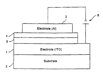
The Hole Tran nort/Elecrrnr, Rl~~kin
g~~
Referring to Figure l, the hole transport/electron blocking layer 5 is shown
in
electrical contact with electrode 1 and electron transporting layer 4. This
layer may
3
CA 02307035 1999-07-29
WO 98/40899 PCT/US98/04988
comprise any appropriate polymer, copolymer or oligomer, or derivative
thereof. .An
example of the polymeric hole transport/electron blocking layer may be any
carbazole-coating polymer, such as polyvinyl carbazole) (PVK).
Figure 2 shows the chemical structure of the repeating units of polymers that
may be used in accordance with one embodiment of the present invention,
structure
(b) being that of a repeating unit of polyvinyl carbazole) (PVK).
The Electron Transportint Layer
Also shown in Figure 1 is the electron transporting layer 4 shown in
electrical
contact with electrode 3 and hole transport/electron blocking layer 5.
The polymeric layer acting as the electron transporting emissive layer may
comprise any appropriate polymer, copolymer or oligomer, or substituted or
wrapped
derivatives thereof, such as poly(pyridyl vinylene phenylene vinylenes),
poly(dithienylene phenylenes), such as shown in the examples below. This layer
may
comprise, for instance, a poly(pyridyl vinylene phenylene vinylene) (PPyVPV)
polymer, copolymer or oligomer, or derivative thereof, such as shown in
structure (a)
of Figure 2, being that of a repeating unit of a poly(pyridyl vinylene
phenylene
vinylene) (PPyVPV) derivative (i.e., PPyVP(COOCi2H,;)zV)
Figure 7(a), 7(b) and 7(c) show other examples of copolymers and their
derivatives that may be used as the electron transporting emissive layer.
The electron-withdrawing nature of the side groups, such as those in the
copolymer PPyVP(COOC,zH2s)2V, render the copolymer more resistive to oxidation
than the unsubstituted copolymer, and are thus preferred.
4
CA 02307035 1999-07-29
WO 98/40899 PCTNS98/04988
The copolymers are soluble in common organic solvents such as w
tetrahydrofuran (TI-IF), xylene, and chloroform.
I-Iole-Injectine Electrodes
With respect to such alternative materials and referring to Figure 1, the hole-
s injecting electrode 1 may be of any appropriate material. Electrodes may be
fashioned from any suitable conductive material including metals, degenerate
semiconductors, and conducting polymers including, but not limited to, a wide
variety
of conducting materials such as ( 1 ) indium-tin-oxide ("ITO"), (2) metals
such as gold,
aluminum. silver, copper, indium and magnesium, (3) alloys such as magnesium-
silver, (4) conducting fibers such as carbon fibers, and (5) highly-conducting
organic
polymers such as highly-conducting doped polyaniline, highly-conducting doped
polypyrrole, polyaniline salt (such as PAN-CSA) or other doped pyridyi
nitrogen-
containing polymer, such as polypyridylvinylene.
Electron-Injecting Electrodes
With respect to such alternative materials and referring to Figure l, the
electron-injecting electrode 3 may be of any appropriate material. Electrodes
may be
fashioned from any suitable conductive material including metals, degenerate
semiconductors, and conducting polymers including, but not limited to, a wide
variety
of conducting materials such as ( 1 ) metals such as aluminum, calcium,
silver, copper,
indium and magnesium, (2) alloys such as magnesium-silver and lithium-
aluminum,
(3) conducting fibers such as carbon fibers, and (4) highly-conducting organic
polymers such as highly-conducting doped polyaniline, highly-conducting doped
polypyrrole, polyaniline salt (such as PAN-CSA) or other doped pyridyl
nitrogen-
containing polymer, such as polypyridyivinylene.
5
CA 02307035 1999-07-29
WO 98/40899 PCT/US98/04988
In typical applications where the device is used for illumination and display,
a~
least one of the electrodes may be fashioned from a transparent material such
as ITO
or a partially transparent material such as highly-conducting doped
polyaniline.
Partially transparent electrodes may be used to advantage to filter or clip
unwanted
frequencies of light coming from the light-emitting material.
It is noted that it is not necessary that the electrode material be
transparent or
even partially transparent. In cases where the electrode materials are opaque
to the
emitted light, light emission from the edge of the device may be utilized in,
for
example, edge-lighted displays or in coupling applications such as in coupling
the
device to an optical fiber.
a strate
For ease of manufacture and safety purposes, it is often desirable to form
the device on a substrate which also serves to protect and often to insulate
(both
physically and electrically) the device during use. The substrate layer may be
any
appropriate material, such as glass or clear electrically insulating plastic
substrates
which are preferred when the device is used for lighting and display purposes.
A DC
driven device is especially suitable for light emission from both sides of the
device in
which case electrode materials, as well as any protective substrates that may
be used
with one or both electrodes, are at least partially transparent. The substrate
layer is
shown in Figure 1 as substrate layer 2.
The Source of 1~ lectrical nPr~v
The devices of the present invention may be operated by any appropriate
source of electrical energy 8 shown in Figure t.
b
CA 02307035 1999-07-29
WO 98/40899 PCT/US98/04988
The first electrode and the second electrode are electrically connected to-a
potential difference. Por instance, the first electrode can be connected to a
positive
potential (anode) while the second electrode is connected to a negative
potential
(cathode)
The electrodes 1 and 2 are connected to a voltage source 8 by means of
suitable electrical connectors or contacts. Such electrical connectors and
contacts are
conventional in the art and may include wire leads, printed circuit
connectors, spring
clips, snaps, solder, wrapped posts, conducting glues, etc. It is also to be
understood
that the electrical connector or contact can be the electrodes 1 and 3
themselves. That
is, the potential difference from voltage source 8 may be applied directly to
the
electrodes in which case electrodes 1 and 3 may become the electrical contact
or
connector.
The devices of the present invention may feature a relatively low turn-on and
operating DC voltage of less than about 24 volts, depending upon polymeric
thickness. More preferably, a turn-on and operating voltage of less than about
12, and
even less than about ~ volts may be achieved. Such low voltages make these
devices
particularly advantageous for use in toys, as commercial light strips such as
found on
airplanes and in theaters, as signs, and as flat panel displays for computer
and
television use. Devices of the present invention may be operated with AC
current in
which case the device will operate when current is flowing in the forward
direction.
Advantages of the devices of the present invention include that the light
emission occurring relatively further away from the electrodes (i.e., such as
the Al and
ITO electrodes), which may tend to quench luminescence.
7
CA 02307035 1999-07-29
WO 98140899 PC'T/US98/04988
Another advantage is that the charge is confined at the polymer/polymer -
interface by the electron blocking nature of the electron blocking layer
(i.e., such as
the PVK layer). This leads to an increased probability of electron-hole
recombination
due to the density of electrons and holes at the interface.
The devices of the present invention also feature a sequestered
polymer/polymer interface that protects the emission from degradation due to
oxygen
that tends to change the vinylene units to carbonyl units which in turn
quenches the
luminescence.
The devices of the present invention may also be used to produce electrically
or optically pumped laser light. By using a polymeric layer arrangement of the
present invention, it is possible to concentrate the energy spatially at the
interface.
This would allow attainment of lasing at relatively low pump thresholds,
whether the
device is electrically or optically pumped. Optically pumped lacing may be
attained
by irradiating the interfacing polymer layers with sufficient light intensity
at
sufficiently short wavelength to cause photoexcitation of the exciplex.
Electrically
pumped lacing may be attained by supplying enough current density to create a
critical density of exciplexes sufficient to cause lasing, which will depend
upon
geometrical factors understood in the art.
The foregoing and other advantages of the invention will become apparent
from the following disclosure in which one or more preferred embodiments of
the
invention are described in detail and illustrated in the accompanying
drawings. It is
contemplated that variations in procedures, processing, structural features,
arrangement of parts, experimental design, ingredients, compositions,
compounds,
8
CA 02307035 1999-07-29
WO 98/40899 PCT/IJS98/04988
and elements may occur to a person skilled in the art without departing from
the scop~-
of or sacrificing any of the advantages of the invention.
brief Description of the Drawin ~
Figure 1 is a general schematic of a tight-emitting device of the present
invention.
Figure 2 shows the chemical structure of the repeatin; units of polymers that
may be used in accordance with one embodiment of the present invention;
structure
(a) being that of a repeating unit of a poly(pyridyl vinylene phenylene
vinylene)
(PPyVPV) derivative (i.e., PPyVP(COOC~.,H2;)ZV), and structure (b) being that
of a
repeating unit of polyvinyl carbazole) (PVK).
Figure 3 is a graph showing the photoluminesence spectra of
PPyVP(COOC~ZH2;),V at 2.8 eV excitation energy (-), a bilayer of PVK and
PPyVP(COOC~,HZs)ZV at 3.6 eV excitation energy (0) and 2.8 eV excitation
energy
(O), and PVK at 3.6 eV excitation energy (...), all on quartz substrates, in
accordance
with one embodiment of the present invention.
Figure 4 is a graph showing the photoluminesence spectra of a bilayer of PVK
and the copolymer PPyVP(COOC,zH2s)ZV in a light-emitting device in accordance
with one embodiment of the present invention, as a function of both excitation
and
emission energy.
Figure ~ shows graphs of the absorption and photoluminesence excitation
(PLE) spectra of (a) a single layer of the copolymer PPyVP(COOCi2H2s)ZV {- _ _
_)~
(b) a single layer of PVK ( . . . . ), and (c) a bilayer of PVK and the
copolymer
9
CA 02307035 1999-07-29
WO 98/40899 PCT/US98/04988
PPyVP(COOC,ZHzs)ZV (-) in a light-emitting device in accordance with one -
embodiment of the present invention.
Figure 6 shows graphs of the electroluminesence and photoluminesence
spectra of a light-emitting device in accordance with one embodiment of the
present
invention. Also shown are the current density vs. voltage and brightness vs.
voltage
data.
Figure 7 shows the chemical structures (a) - (e) of the repeating units of
copolymers that may be used in accordance with several embodiments of the
present
invention; structure (a) shows three alternative derivatives according to
variations in
moiety R; such that R; = OCi~H3;, C,zH,; or COOCi~H~s, designated
structures"ax,"
"ay" and "cx," respectively; structure (b) shows an unsubstituted "wrapped"
copolymer, designated wPPyVPV; structure (c) shows three alternative
derivatives of
"wrapped" copolymers according to variations in moiety R; such that R; =
OCi6H;3,
C~ZH~; or COOC,ZH,;, designated wPPyVPV(ax), wPPyVPV(ay), and
1 ~ wPPyVPV(cx), respectively . Structure (d) of Figure 7 is designated wPTP
and
structure (e) is designated wPDTP.
Figures 8a through 8e are graphs showing the photoluminesence and PLE
spectra of several polymer/copolymer materials that may be used in accordance
with
several embodiments of the present invention.
?0 Figure 9 is a gt'aph ShOWlllg the photoluminesence spectra of several
wPPyVPV(ax)/PVIC blends in accordance with several embodiments of the present
invention; graph (a) showing PL film efficiency as a function of wPPyVPV(ax)
content, and graph (b) showing PL relative intensity and normalized PL
intensity as a
Function of energy.
CA 02307035 1999-07-29
WO 98/40899 PCTNS98104988
Figures I O and 11 show the PL spectra of single layers of PVK and each of the
copolymers along with the corresponding bilayers. Figure 10 shows (a) the film
PL
spectra of PPyVPV (structure ay; solid lines), PVK (~) and a bilayer of
PVK/PPyVPV (structure ay) (dashed lines); and (b) the film PL spectra of
PPyVPV
(structure cx; solid lines), PVK (~) and a bilayer of PVK/PPyVPV(structure ex)
(dashed lines). Figure 11 shows the PL for single layer films (solid lines),
bilayer
films (dashed lines) and PVK(1), for three copolymers wPPyVPV(ax),
wPPyVPV(ay), and wPPyVPV.
Figure 12 shows the EL of two bilayer devices (see caption) along with the
i 0 corresponding PL results. The EL and PL of these bilayer devices are
substantially
the same, demonstrating that the EL originates from the exciplex states formed
at the
interface between the hole- and electron-transporting layers.
Detailed Description of the Preferred Embodiments
In accordance with the foregoing summary of the invention, the following
describes preferred embodiments of the present invention which are presently
considered to be the best mode of the invention.
Example of a Sam lie Pre aration
A conjugated polymer light-emitting device consists of an emitting material
(layer) sandwiched between two electrodes, one of which is preferably
transparent.
Indium-tin-oxide was used as the positive transparent electrode (anode) and
aluminum
was most often used as the negative electrode (cathode). The ITO-coated glass
(commercially available from Donnelly Applied Films or Deita Technologies
Ltd.)
11
CA 02307035 1999-07-29
WO 98/40899 PCT/US98/04988
was purchased in large sheets 12" x 12". The ITO-coated glass was cut into
appropriate size pieces (typically 2 cm x 2 cm) by the glass shop.
Each individual substrate then was etched before use. The etching was done
with a solution of 20 % HCI, ~% HN03, and 75% distilled water, by volume,
heated
to ~50 to 60° C. After etching, the ITO substrates were cleaned.
The emitting polymer was then spin-coated onto the clean etched ITO
substrate or on top of a previously spin coated layer of PVK from the
appropriate
solvents. PPy was cast from formic acid solution and the copolymers of PPyV
and
PPV were cast from tetrahydrofuran (THF), xylene or chloroform.
Solution concentrations of the copolymer were typically s-10 mg/ml. The
powders were weighed on a balance after which the appropriate solvent was
added.
The solutions were stirred with a spin bar for at least 1 hour or until the
powders were
almost completely dissolved. The solutions were filtered with either a 1
micron or 0.2
micron pore filter and stored in a hood until used. In the class 100
cleanroom, the
films were made by dropping 3 - 5 drops of solution from a pipette on to the
ITO
glass substrate. The substrate was then immediately spun at speeds ranging
from
1000 to 2000 rpm. Following spin-coating the top electrode (Al or Au) was
vacuum
deposited (evaporated) at pressures below ~10-6 torr. A mask was used to
evaporate
the appropriate electrode pattern. To prevent damage due to heating during
evaporation, the substrates were
mounted on a cold water cooled stage during deposition. In addition,
evaporation
rates were ~0.5- I .4 ~./s for the first I 00 ~ of deposition and then
increased to ~3-5
~/s until the desired thickness was reached (usually 1000 to 2000 t~).
12
CA 02307035 1999-07-29
WO 98/40899 PCT/US98104988
The device performance was improved by inserting either a hole-transporting-
layer between the anode and emitter or an electron-transporting layer between
the
emitter and cathode. The most commonly used hole-transporting layer, poly(9-
vinyl
carbazole) (PVK), was cast from THF (10 mg/ml) onto the ITO at 3000 rpms. When
fabricating multilayer devices, the choice of solvents is critical. The second
layer
should not dissolve the original layer and the solvents should be compatible
enough to
make uniform films.
Each of the copolymers was treated identically although the solution
concentration may have been slightly different. For the PL experiments the Al
electrodes were not evaporated.
After fabrication some devices are annealed at 80° C for 2 hours.
The photoluminesence and electroluminesence results were as follows:
Figure 3 is a graph showing the photoluminesence spectra of
PPyVP(COOC,2H2;)ZV at 2.8 eV excitation energy (-), a bilayer of PVK and
PPyVP(COOC,ZH2;)ZV at 3.6 eV excitation energy (Cl) and 2.8 eV excitation
energy
(O), and PVK at 3.6 eV excitation energy (...), all on quartz substrates, in
accordance
with one embodiment of the present invention. The PL of single PVK layers
excited
at 3.6 eV has a peak emission energy at 3.05 eV, similar to previous reports
of the PL
of PVK. The PL for single layer copolymer films excited at 3. i eV shows an
emission peak at 2.05 eV. The bilayer when excited at an energy less than the
absorption edge of the PVK, but greater than the absorption edge of the
copolymer,
shows PL peaked at the same energy as for the copolymer along with a low
intensity
tail to the blue side. When the bilayer was excited at energy equivalent to
the
excitation energy for the single PVIC layer (3.G eV), the PL emission spectrum
13
CA 02307035 1999-07-29
WO 98/40899 PCT/US98/04988
contains contributions from both single layers (3.05 eV and 2.05 eV), as well
as fron3--
a completely new species, which may be identified with an exciplex. To the low
energy side of the exciplex PL is a weak shoulder near the PL energy for the
single
layer of the copolymer.
Figure 4 is a graph showing the photoluminesence spectra of a bilayer of PVK
and the copolymer PPyVP(COOC~.,H2;),V in a light-emitting device in accordance
with one embodiment of the present invention, as a function of both excitation
and
emission energy. The 3D plot shows three prominent features: a peak due to the
PVK (excitation energy from 3.6 to 4.2 eV, emission energy 2.8 to 3.4 eV), a
peak
due to the copolymer (excitation energy from 2.4 to 3.0 eV, emission energy
1.8 to 2.2
eV), and the exciplex peak (excitation energy from 3.6 to 4.2 eV, emission
energy 2.2
to 2.8 eV).
At excitation energies above 3.6 eV the PL due to the exciplex and PVK are
apparent,
but if the excitation energy is lowered below 3.4 eV these peaks have
essentially
disappeared. As the excitation energy is further lowered into the peak
absorption of
the copolymer, PL from the copolymer strongly predominates (excitation energy
2.6
to 3.0 eV and principal emission energy I.8 to 2.2 eV). The 3D plot shows
three
prominent features: a peak due to the PVK (excitation energy from 3.6 to 4.2
eV,
emission energy 2.8 to 3.4 eV), a peal: due to the copolymer (excitation
energy from
2.4 to 3.0 eV, emission energy 1.8 to 2.2 eV), and the exciplex peak
(excitation
energy from 3.6 to 4.2 eV, emission energy 2.2 to 2.8 eV).
Figure 5 shows graphs of the absorption and photoluminesence excitation
(PLE) spectra of (a) a single layer of the copolymer PPyVP(COOC~zH25),V, (b) a
single layer of PVI<, anti (c) a bilayer of PVK and the copolymer
14
CA 02307035 1999-07-29
WO 98/40899 PCT/US98/04988
PPyVP(COOCi2H25)ZV, on quartz substrates, in a light-emitting device in
accordance'
with one embodiment of the present invention. The PLEs were recorded at 2.05,
3.05,
and 2.~5 eV, respectively. The copolymer absorption is 5 times less than
shown.
The absorption and photoluminescence excitation (PLE) spectra are shown in
Figures Sa and Sb. The onset of the absorption of the single PVK layer is at
about 3.5
eV and shows two spectral features at 3.6 and 3.75 eV similar to previous
reports.
The PLE of PVK follows the absorption showing nearly identical features. The
absorption and PLE of the copolymer peak at 2.95 eV, with the onset at about
2.4 eV.
The absorption of the bilayer is the sum of the single PVK layer absorption
and the
single copolymer absorption and shows both the copolymer peak at 2.9~ eV and
the
PVK peaks at 3.6 and 3.75 eV. The PLE of the bilayer is also the sum of the
PVK
PLE and the copolymer PLE and shows both the PVK spectral features and the
copolymer peak, although the copolymer peak is shifted to slightly higher
energy.
The lack of any new absorption or PLE features in the bilayer film implies
that the
new species is not directly accessible from the ground state of the copolymer
or PVK.
and is thus consistent with the assignment of an exciplex.
The PL, PLE and absorption were measured on the same films making it
possible to estimate the relative PL quantum efficiencies of the copolymer
emission
and the exciplex emission. The copolymer absolute PL efficiency was reported
previously to be 18%. f~ lower bound on the quantum efficiency of the exciplex
was
calculated to be 1 S-20%, nearly the same as the copolymer efFciency.
Figure 6 shows graphs of current-voltage(-) and brightness-voltage {~)
characteristics of a typical bilayer light-emitting device. Inset: PL (...)
and EL (-)
CA 02307035 1999-07-29
WO 98/40899 PCT/US98/04988
of a bilayer light-emitting device, in accordance with one embodiment of the
present-
invention.
Bilayer devices were fabricated using ITO as the anode and aluminum as the
cathode. The inset of Figure 6 shows the EL spectrum of a typical device with
the PL
spectrum from the same device. The devices can easily be seen in a bright lit
room,
appear bright green to the eye, and have internal duantum efficiencies of ~
0.1-0.~%.
Although the PL efficiencies are comparable, the EL efficiency of the bilayer
configuration ~ 0.1-0.~% is much greater than for a single layer device which
has an
EL efficiency of less than 0.0001%. The similarity between the PL and EL of
the
bilayer device demonstrates that the exciplex is responsible for the EL
emission.
Figure 6 shows the current density-voltage and brightness-voltage
characteristics for a
typical bilayer device. The turn-on voltage of the bilayer devices depends on
the
thickness of the polymer layers and in this case is ~ 18 volts, with the
brightness
following the current. The generality of this concept has been demonstrated
using
1 ~ several other pyridine-based copolymers. Through the use of polyaniline
network
electrodes, the threshold voltage was lowered to below 5 volts while
maintaining the
same efficiency.
The increase in efficiency of the bilayer device compared to the single layer
device appears to be due primarily to charge confinement at the PVK/copolymer
interface. The electrons are injected from the A1 electrode into the
conduction band of
the copolymer, but are conl7ned when they reach the electron blocking PVK.
Also,
the holes are injected into the valence band of the PVK and are confined at
the
interface. The electron and hole blocking at the interface enhances exciplex
emission.
That the electron and holes are unable to easily conduct through both layers
leads to a
16
CA 02307035 1999-07-29
WO 98/40899 PCT/US98/04988
small current density (< or ~ 1 mA/mmz) and hence a greatly increased
efficiency. I-rr
addition, the buried interface implies that most of the radiative
recombination will
occur at the interface and away from the EL quenching electrodes.
A wide range of devices were fabricated with a variety of different emitting
polymers and hole transport layers, including bilayer devices with the
following
emitter layers: poly(pyridyl vinylene), PPyVP(R)zV (R=OC,6H33, R=Cl,H2s,
R=COOC,ZH,;), a strapped copolymer PPyVP(R).,V (with R=H, R=OC,6H3;,
C,,H,;), poly(thienylene phenylene) with a strap, and poly(dithienylene
phenylene)
with a strap. The molecular repeat unit of these copolymers is shown in Figure
7,
structures (a) - (e).
Figures 8a through 8e are graphs showing the electroluminesence and
photoluminesence spectra of several polymer/copolymer materials that may be
used in
accordance with several embodiments of the present invention.
In Figure 8(a) the polymer referred to as "Ci.,H,;" is that shown in Figure
7(a)
where R=CizH,;.
In Figure 8(b), the polymer is that shown in Figure 7(a) wherein
R=COOC, ZHz;.
In Figure 8(c), the polymer referred to as"D40" is that shown in Figure 7(c)
wherein R=OC,GH;3.
In Figure 8(d) the polymer referred to as "D41" is that shown in Figure 7(c)
wherein R= C~ZH2;.
In Figure 8(e), the polymer referred to as ''D 112" is that shown in Figure
7(b).
In each case, the PVI< was used as the hole-transporting layer.
17
CA 02307035 1999-07-29
WO 98/40899 PCT/US98/04988
Blends of these polymers/copolymers with PVK show PL emission due te-
exciplex formation (Figure 9) and are expected to show EL emission from
exciplexes.
The generality of using pyridyl containing polymers as the emitting polymer
thus has been shown and it is expected that the other light-emitting polymers
such as
polyparaphyenylene (PPP), polyparaphenylene vinylenes (PPV), polythiophenes
(PT)
and their derivatives and/or copolymers to behave similarly based on chemical
and
electronic similarities. Other hole-transporters such as PPPs, PPVs,
polymethyl
methacrylate, polystyrene, polyethylene, polyethylene teraphthalate) and
blends of
these materials are expected to behave similar to PVK.
Figure 9 is a graph showing the photoluminesence spectra of several
wPPyVPV(ax)/PVK blends in accordance with several embodiments of the present
invention; graph (a) showing PL film efficiency as a function of wPPyVPV(ax)
content, and graph (b) showing PL relative intensity and normalized PL
intensity as a
function of energy.
Figures 10 and 11 show the PL spectra of single layers of PVK and each of the
copolymers along with the corresponding bilayers. Figure 10 shows (a) the film
PL
spectra of PPyVPV (structure ay; solid lines), PVK (~) and a bilayer of
PVK/PPyVPV (structure ay) (dashed lines); and (b) the fllln PL spectra of
PPyVPV
(structure cx; solid lines), PVK (~) and a bilayer of PVK/PPyVPV(structure cx)
(dashed lines). Figure 11 shows the PL for single layer films (solid lines),
bilayer
films (dashed lines) and PVIC(~), for three copolymers wPPyVPV(ax),
wPPyVPV(ay), and wPPyPV.
Figure 12 shows the EL of two bilayer devices (see caption) along with the
corresponding PL results. The IrL and PL of these biiayer devices are
substantially
18
CA 02307035 1999-07-29
WO 98/40899 PCT/US98/04988
the same, demonstrating that the EL originates from the exciplex states formed
at the
interface between the hole- and electron-transporting layers.
In summary, heterojunctions of PVK and PPyVP polymers show a strong
photoluminescence and electroluminescence feature due to exciplex emission at
the
interface. The absorption and PLE spectra and have shown that the exciplex is
not
directly accessible from the ground state. The exciplex is also the primary
species of
electroluminescence emission in the bilayer devices. The efficiency of the
bilayer
devices is greatly enhanced over single layer devices due to charge
confinement and
exciplex formation and emission at interface.
Thus, the bilayer devices of the described embodiment of the present invention
use PVK as the hole transport layer and a derivative of the copolymer PPyVPV
as the
emitter layer. Absorption, photoluminesence and electroluminesence results are
consistent with emission due to exiplex formation between the PVK and PPyVPV
copolymer. The PL and EL of bilayer films are dramatically different from that
of the
1 S single layer.
The preferred embodiments herein disclosed are not intended to be exhaustive
or to unnecessarily limit the scope of the invention. The preferred
embodiments were
chosen and described in order to explain the principles of the present
invention so that
others skilled in the art may practice the invention. Having shown and
described
preferred embodiments of the present invention, it will be within the ability
of one of
ordinary skill in the art to make alterations or modifications to the present
invention,
such as through the substitution of eduivalent materials or structural
arrangements, so
as to be able to practice the present invention without departing from its
spirit as
19
CA 02307035 1999-07-29
WO 98/40899 PCT/US98/04988
reflected in the appended claims. It is the intention, therefore, to limit the
inventiort-
only as indicated by the scope of the claims.