Note: Descriptions are shown in the official language in which they were submitted.
CA 02307240 2000-OS-O1
MATCHLINE SENSE CIRCUIT AND METHOD
FIELD OF THE INVENTION
The present invention relates to content addressable memory. In particular,
the
present invention relates to a matchline circuit and matchline sensing circuit
for detecting a
signal on a matchline.
BACKGROUND OF THE INVENTION
In many conventional memory systems, such as random access memory, binary
to digits (bits) are stored in memory cells, and are accessed by a processor
that specifies a linear
address that is associated with the given cell. This system provides rapid
access to any
portion of the memory system within certain limitations. To facilitate
processor control, each
operation that accesses memory must declare, as a part of the instruction, the
address of the
memory cell/cells required. Standard memory systems are not well designed for
a content
15 based search. Content based searches in standard memory require a software
based
algorithmic search under the control of the microprocessor. Many memory
operations are
required to perform a search. These searches are neither quick nor efficient
in using
processor resources.
To overcome these inadequacies an associative memory system called Content
2o Addressable Memory (CAM) has been developed. CAM allows cells to be
referenced by
their contents, so it has first found use in lookup table implementations such
as cache
memory subsystems and is now rapidly finding use in networking systems. CAM's
most
valuable feature is its ability to perform a search and compare of multiple
locations as a
single operation, in which search data is compared with data stored within the
CAM.
25 Typically search data is loaded onto search lines and compared with stored
words in the
CAM. During a search-and-compare operation, a match or mismatch signal
associated with
each stored word is generated, indicating whether the search word matches a
stored word or
not.
A CAM stores data in a matrix of cells, which are generally either SRAM based
3o cells or DRAM based cells. Until recently, SRAM based CAM cells have been
most
common because of their simple implementation. However, to provide ternary
state CAMS,
ie. where the match operation returns a "0", "1" or "don't care" result,
ternary state SRAM
based cells typically require 16 transistors compared to DRAM based cell of 6
transistors. As
CA 02307240 2000-OS-O1
a result, ternary state SRAM based CAMs have a much lower packing density than
ternary
DRAM cells.
To provide the desired search and compare function in a DRAM or SRAM based
CAM, matchline sensing circuits are required. Each matchline sensing circuit
returns the
appropriate state of its matchline, and the outputs of each matchline sensing
circuit can be
subsequently processed to determine the existence and address of a match. A
prior art
matchline sensing circuit is disclosed in commonly owned US Patent Application
No.
filed , the contents of which are incorporated herein by reference. In the
matchline sensing scheme of the prior art, each matchline is initially
precharged high to the
1o full VDD supply. A matchline will be discharged to ground if the contents
of its stored word
do not match, or mismatch, the search word, but will remain at the VDD supply
if the stored
word matches the search word. Each matchline potential level is compared to a
fixed
reference voltage, and the matchline sensing circuit generates a result from
the comparison.
There are several disadvantages in the matchline sensing scheme of the prior
art.
Charge sharing between the VDD precharged matchline and the CAM cells will
cause the
matchline potential to fluctuate as a function of the previous cycle search
data. This can
cause a matchline sense circuit to generate a false result from the subsequent
comparison.
This problem becomes increasingly significant as CAM array cell densities
increase.
To attain higher packing density, CAM cell transistors use minimum feature
sizes.
2o Hence the current capacity of a CAM cell to ground a fully precharged
matchline is small,
resulting in very slow discharge of the matchline, and increasing the overall
search and
compare operation of the CAM chip. Inherent parasitic capacitance of the
matchline
compounds this problem, which increases as CAM arrays become larger.
The optimal sensing margin for the matchline sense circuit should be
sufficient for
the circuit to easily distinguish if the matchline potential level is above or
below the reference
voltage. This optimal sensing margin is attained at the time when the
matchline voltage level
has decreased to a potential level well below the reference voltage.
Unfortunately, the poor
voltage discharge rate of the matchline previously described only allows
accurate sensing to
be performed at a prolonged time after the matchline voltage begins to fall.
3o Sensing can be performed at a time shortly after the matchline voltage
drops below
the reference voltage if the reference voltage is maintained at a precise
level. This is difficult
to accomplish due to process variations in the fabrication of the CAM chip,
which can alter
the reference voltage level beyond the original design specifications.
CA 02307240 2000-OS-O1
Power consumption of the prior art matchline sense circuit is high since any
discharged matchlines must be precharged back to VDD level in preparation for
the next
search and compare operation. Power consumption can be expressed as
P ~ CML x VDD x OV x f where CML is the matchline parasitic capacitance, OV is
the
difference between VDD and the discharged potential level of the matchline at
the sensing
time and f is the frequency of operation. If 0V is large, then the power
consumed will be
large, possibly exceeding the power dissipation capability of the package. The
prior art match
line circuit required all search lines to be held at a low logic level during
the match line
precharge phase. Even if search data did not change substantially during
successive search
to operations considerable power was consumed as search lines were brought low
at the
beginning of the match line precharge phase and brought high again for the
actual search
operation.
There is clearly a need for a matchline sensing circuit capable of consuming
very
little power and detecting matchline potential levels accurately at high
speed.
SUMMARY OF THE INVENTION
It is an object of the present invention to obviate or mitigate at least one
disadvantage of the prior art. In particular, it is an object of the present
invention to provide a
less complex sensing circuit, a method of using such a circuit, and a content
addressable
2o memory using such a sensing circuit, that detects voltage levels quickly
and accurately.
In a first aspect, the present invention provides a sensing circuit for
detecting a
voltage. The sensing circuit has a sense line initially precharged to a first
voltage level. A
current source is operatively connected to the sense line, and a timing
circuit is operatively
connected to the current source to switch the current source between an on
state and an off
state to thereby ramp the sense line from the first voltage level to a second
voltage level. A
sense amplifier can then detect the second voltage level to provide a
corresponding output.
Embodiments of the sensing circuit of the present invention provide a
precharge
circuit to precharge the sense line, which can consist of n-channel or p-
channel transistors,
precharged high or low as applicable. In a presently preferred embodiment, the
timing circuit
3o is a reference sensing circuit that includes a dummy sense line initially
precharged to the first
voltage level, and a dummy current source operatively connected to the dummy
sense line,
and to a feedback circuit. The feedback circuit switches the dummy current
source between
the on state and the off state for ramping the dummy sense line between the
first voltage level
CA 02307240 2000-OS-O1
and the second voltage level, in response to a feedback output. A dummy sense
amplifier
detects the second voltage level of the dummy sense line, and provides the
feedback output to
the feedback circuit when the second voltage level is detected. The reference
sensing circuit
can be precharged as described above for the sensing circuit. In the presently
preferred
embodiment, the sense amplifier includes a sense transistor coupled between an
output node
and a source line and having a threshold potential level. The sense transistor
is turned on
when the sense line potential level reaches the second voltage level. The
sense transistor can
also be an n-channel or p-channel transistor, as applicable. In a presently
preferred
embodiment, a propagation delay circuit delays the timing circuit from
switching the current
1o source between the on state and the off state. The propagation delay
circuit can be a non-
inverting buffer, or a capacitor.
The sensing circuit of the present invention can also include a delay circuit
for
inhibiting the sense transistor from turning on. The delay circuit can include
a coupling
circuit for forming a conduction path between a tail line and ground, to raise
the threshold
potential level of the sense transistor. The coupling circuit is at least one
transistor connected
between the tail line and ground. The delay circuit can also include a current
limiting circuit
for reducing the current supplied to the sense line by the current source,
such as a transistor
connected in series with the current source to restrict the supply of current
to the sense line
when a conduction path between the sense line and the tail line is formed.
Generally, the
output of the sensing circuit is maintained by a latching circuit, which can
be either a full or
half latch.
In a further aspect of the present invention, there is provided a method for
detecting
a voltage level. The method consists of precharging a sense line to a first
voltage level,
ramping the voltage level of the sense line for a predetermined time from the
first voltage
level to a second voltage level, detecting the second voltage level of the
sense line; and
providing an output corresponding to the detected second voltage level.
In yet another aspect of the present invention, there is provided a method for
detecting a match or mis-match condition of match lines. This method consists
of setting the
match lines in the mis-match condition by precharging the match lines to a
"miss" voltage
level, and ramping only match condition match lines to a "hit" voltage level.
A further aspect of the present invention provides a sensing circuit for
detecting a
voltage in a content addressable memory. The sensing circuit consists of a
first and second
voltage supplies with first, second and third transistors of a first type
connected in series
between the first voltage supply and a match line, the gate of the second
transistor of the first
CA 02307240 2000-OS-O1
type being connected to a bias voltage. A plurality of pairs of series
connected search and
compare transistors of a second type are connected in parallel between the
match line and a
tail line. The gate of each search transistor is connected to a search line,
the gate of each
compare transistor is connected to a memory cell, and the tail line is
connected to the gate of
the third transistor of the first type. A first transistor of the second type
is connected between
the match line and the second voltage supply. A second transistor of the
second type is
connected between an intermediate output node and the tail line, and the gate
of the second
transistor connected to the match line. A third transistor of the second type
is connected
between the tail line and the second voltage supply. A first enable signal is
connected to the
to gates of the first transistor of the first type, the first transistor of
the second type and the third
transistor of the second type. A first logic gate has a first input connected
to the intermediate
output node, a second input connected to a second enable signal, and an
output. A first
inverter couples the output to the intermediate output node, and a reference
circuit generates
the first enable signal.
Another aspect of the present invention provides a content addressable memory.
The content addressable memory includes an array of content addressable memory
cells
arranged in rows and columns, an address decoder, data access circuitry; and a
matchline
sensing circuit as described above.
2o BRIEF DESCRIPTION OF THE DRAWINGS
Preferred embodiments of the present invention will now be described, by way
of
example only, with reference to the attached Figures, wherein:
Figure 1 shows a block diagram of a CAM according to an embodiment of the
present invention;
Figure 2 shows a schematic of a DRAM based CAM cell;
Figure 3 shows a schematic of a matchline and associated functional circuits
/blocks of the prior art;
Figure 4 shows a plot of sense margin voltage versus time for the schematic of
figure 3;
3o Figure 5 shows a block diagram of the CAM array and matchline sense circuit
block of figure 1 in accordance with a first embodiment of the present
invention;
Figure 6 shows a schematic a CAM array matchline circuitry and reference
matchline circuitry in accordance with a second embodiment of the present
invention;
CA 02307240 2000-OS-O1
Figure 7 shows a generic schematic of a matchline sense circuit in accordance
with
a third embodiment of the present invention;
Figure 8 shows a schematic of a matchline sense circuit in accordance with a
fourth
embodiment of the present invention;
Figure 9 shows a schematic of a matchline sense circuit in accordance with a
fifth
embodiment of the present invention;
Figure 10 shows a schematic of a matchline sense circuit in accordance with a
sixth
embodiment of the present invention;
Figure 11 shows a schematic of a CAM array and matchline sense circuits in
accordance with a seventh embodiment of the present invention;
Figure 12 shows a sequence diagram of the CAM search-and-compare operation
according to the present invention; and
Figure 13 shows a plot of the matchline voltage versus time for a single mis-
match
and match conditions.
DETAILED DESCRIPTION OF THE INVENTION
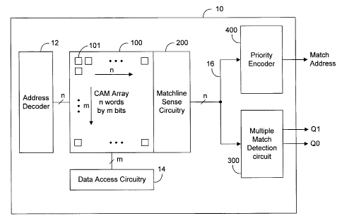
A typical CAM block diagram is shown in Figure 1. The CAM 10 includes a
matrix, or array 100, of CAM cells 101 arranged in rows and columns, where,
for a ternary
CAM, each cell stores one of three states: logic "1 ", logic "0" and "don't
care", actually
2o storing 2 bits of data. A predetermined number of CAM cells 101 in a row
store a word of
data. In the CAM array 100 of Figure 1, there are n rows and m columns, where
n and m are
integer numbers. An address decoder 12 is used to select any row within the
CAM array 100
to allow data to be written into or read out of the selected row although most
commonly, data
is written or loaded into the CAM and searched. The bidirectional data access
circuitry 14
transfers data (DATA) between the CAM array 100 and the data pins (not shown)
of the
CAM chip, for access by an external processor. Located adjacent to the CAM
array 100 for
each row is matchline sense circuitry block 200. Matchline sense circuitry
block 200
comprises n matchline sense circuits and is used during search-and-compare
operations for
outputting an n-bit result 16 indicating a successful or unsuccessful match of
a search word
3o against the stored word. The matchline sense circuitry block results 16 for
all rows are
processed by the priority encoder 400 to generate an address (Match Address)
corresponding
to the location of a matched word. Since it is possible that more than one row
will match the
search word, the priority encoder 400 generates the lowest physical address
corresponding to
a matched word. Acting in parallel with the priority encoder 400 is a multiple
match
CA 02307240 2000-OS-O1
detection circuit 300, which assesses the matchline sense circuit results 16,
and produces a
two bit output Ql, QO representing the cases where there are no matches, only
one match and
two matches or more.
A typical ternary DRAM type CAM cell 101 is shown in Figure 2. Cell 101 has an
n-channel search transistor 102 connected in series with an n-channel compare
transistor 104
between a matchline ML and a tail line TL. A search line SL1 is connected to
the gate of
search transistor 102. N-channel access transistor 106 has a gate connected to
a wordline
WL and is connected in series with capacitor 108 between bitline BL1 and cell
plate voltage
potential VCP. Charge storage node CELL1 is connected to the gate of compare
transistor
104 to turn on transistor 104 if there is charge stored on capacitor 108 i.e.
if CELL1 is logic
"1". The remaining transistors and capacitor, replicate transistors 102, 104,
106 and capacitor
108 for the other half of the ternary data bit, and are connected to
corresponding lines SL2
and BL2 and are provided to support ternary data storage. Specifically, the
three states are
stored by CELLI and CELL2 as follows: (etc...) 0/0, 0/1, 1/0, 1/l. Lines SL1,
SL2, BL1
and BL2 are common to all cells of the column, and lines ML, TL and WL are
common to
all cells of a word in the row. The tail line TL is typically connected to
ground and all the
transistors are n-channel transistors. The description of the operation of the
ternary DRAM
cell is covered in the aforementioned reference which has been incorporated by
reference. In
general, for a match between search and stored data, there must be no
conduction path
2o between the matchline and the tail line, whereas for a mis-match,
conduction will occur
between the matchline and the tail line.
A ternary SRAM type CAM cell consists of 2 SRAM cells, to store each half of
the
ternary bit, and a pair of search transistors and compare transistors which
duplicate the
function of transistors 102 and 104 in Fig.2. From the point of view of search
operations and
matchline functionality, the SRAM cell performs identically to the DRAM type
CAM.
A simplified row schematic from the CAM array 100 and a corresponding prior
art
matchline sense circuit 202 from the matchline sense circuits 240 are shown in
Figure 3. The
access transistors and storage capacitors from Figure 2 are not shown.
Multiple search and
compare transistors (102 and 104 respectively), having gates connected to
their respective
3o search line SLj and cell storage node CELLi, are connected in parallel to
the common
matchline MLi. A matchline sense circuit 202 receives MLi and produces a
matchline
output ML OUTi for the row. The matchline sense circuit 202 of the prior art
requires
control signals DCPL, BIAS, MLPIZE and SEN for proper operation. For purposes
of
comparison with the present invention, a general description of a prior art
CAM matchline
CA 02307240 2000-OS-O1
sensing scheme will now follow with reference to Figures 1 to 4. After data is
written to the
cells 101 of the CAM array 100 via the bitlines, a search for a specific word
of data in the cell
array can be done. Every matchline MLi of the CAM array 100 is first
precharged to a
positive voltage level, such as VDD, through activation of a pulsed MLPRE
signal. During
precharge of the matchline MLi to VDD, all search lines SLj must be grounded
to turn off all
search transistors 102 of every row, isolating the compare transistors 104
from the matchline
MLi, to ensure that the matchlines MLi precharge to the full VDD level once
the precharge
phase terminates. The search word is then loaded onto the search lines SLo to
SLm and each
cell of a word compares its stored data with the data on its respective search
line. Any cell
1o whose stored data does not match the data on its search lines SLj, called a
mis-match
condition, will have both transistors 102 and 104 turned on to form a current
path between
the matchline MLi and ground. Any cell whose stored data does match the data
on its search
lines SLj, called a match condition, will have no affect on the matchline MLi.
Hence, if each
CAM cell of a row has a match condition, then the matchline MLi for the row
will remain at
the precharge voltage level of VDD. However, if at least one cell of a row has
a mis-match
condition, the precharge voltage of the matchline MLi will slowly discharge to
ground over
time. Since the matchline voltage level is neither stable nor suitable for use
in subsequent
logic circuits, a matchline sense circuit 202 will sense and amplify the
matchline voltage
level to full CMOS voltage levels, for example. The output of the matchline
sense circuit
202, ML OUTi, at a high logic level will indicate that the data of the
respective row matches
the search word. ML OUTi at a low logic level will indicate that the data of
the respective
row has not matched in at least one bit.
The prior art circuit of Figure 3 is subject to the previously mentioned
disadvantages. Charge sharing of the MLi with nodes 110 between search and
compare
transistors 102 and 104 respectively, can cause the MLi potential to fluctuate
undesirably.
The matchline sense circuit 202 may generate a false result of the comparison
due to the
fluctuating MLi potential.
The time required by the matchline sense circuit 202 to sense the MLi
potential is
lengthy. Figure 4 is a plot of the matchline voltage VMLi as a function of
time in the case
3o where a current path is formed between the matchline and ground (in the mis-
match
condition). The matchline sense circuit 202 compares VMLi to a reference
voltage VREF at
a predetermined time, to sense if VMLi is above or below VREF. Matchline sense
circuit
202 will generate a high logic level ML OUTi if VMLi is above VREF, and a low
logic
level ML OUTi if VMLi is below VREF. Sensing can be performed at time tl, but
the
CA 02307240 2000-OS-O1
sense margin is very small and a precise VREF voltage generator is required. A
better sense
margin can be achieved at later time t2 without the need for a high precision
VREF voltage.
However, the time between the start of VMLi falling to t2 is wasteful because
the CAM
remains idle while waiting for the result of the comparison. Contributing to
the prolonged
sense time is the minimum feature size of search and compare transistors 102
and 104. One
conducting pair of search and compare transistors 102 and 104 has a small
current capacity,
hence the discharge of MLi (which begins in a high precharged state) to ground
is very slow.
Shrinking feature sizes will extend the optimal sense time past t2 because the
discharge rate
of VMLi will be further diminished.
to After sensing occurs at time t2, all discharged matchlines MLi must be
precharged
back to the VDD voltage supply by an amount of 0V. All searchlines SLj must be
grounded
during MLi precharge before selected searchlines SLj are raised to the VDD
supply for the
sensing operation. Hence, power consumption will be high due to the repeated
discharge and
precharge of matchlines MLi and searchlines SLj.
Reference will now be made to embodiments of the invention. Generally, the
sensing circuit of the present invention is a low power matchline sense
circuit for fast
detection of a match between a search word and a stored word in the CAM cell
array 100.
This is achieved by setting all matchlines to the default miss voltage level
and only pulling up
the matchlines with a match to the hit voltage level. The matchline sense
circuit 200 of the
2o present invention employs a self timing circuit to generate a control
signal. The control
signal is self activated a$er a predetermined amount of time to end sensing of
the matchlines.
Figure 5 depicts a detailed hierarchical view of the CAM array 100 in
accordance
with a first embodiment of the present invention. CAM cells 101 of the CAM
array 100 are
arranged in rows and columns. CAM cells 101 of a row are connected to a common
matchline Mli, word line WLi and tail line TLi, and CAM cells 101 of a column
are
connected to a common pair of search lines SLj and a common pair of bitlines
BLj, where i
is an integer value between 0 and n, and j is an integer value between 0 and
m. Matchlines
MLi and tail lines TLi are connected to their respective matchline sense
circuits 210. The
matchline sense circuits Z10 also receive control signals ENl, EN2* and BIAS,
and produce
a match signal ML OUTi for its respective row.
At least one row of the CAM array 100 is a reference matchline row 270 having
dummy components constructed identically to the components of a normal
matchline ML
and matchline sense circuit 210. The reference matchline 270 will act as a
timing circuit in
CA 02307240 2000-OS-O1
this embodiment as will be described in more detail below. The reference
matchline row 270
will have a dummy sense, or matchline, a dummy current source, dummy cells, a
dummy tail
line and a dummy matchline sense circuit. The dummy matchline sense circuit
will include a
dummy current source. In Figure 5, the dummy match line is a reference
matchline RML,
the dummy cells are reference CAM cells 150, the dummy tail line is a
reference tail line
RTL, and the dummy matchline sense circuit is a reference matchline sense
circuit 272. The
dummy current source is a current source of the reference matchline sense
circuit 272. The
reference matchline sense circuit 272 receives the same control signals as
matchline sense
circuits 210 but inputs the reference match signal RML_OUT to a current
control circuit
274. The current control circuit 274 acts as a feedback circuit which also
receives control
signal EN2* and generates the ENl control signal.
The reference matchline row 270 generates a self timed control signal, EN1 for
controlling all the matchline sense circuits 210. The time required for RML to
rise between
ground and a predetermined voltage level will be used as a reference time to
compare normal
matchline ML rise times between ground and the same predetermined voltage
level. A
matchline sense circuit 210 will therefore determine if its corresponding
matchline ML rises
at the same rate as the reference rise time, or at a slower rate than the
reference rise time.
This comparison is achieved by resetting all matchlines ML to ground at a cut-
off time
signalled by ENl after RML reaches the predetermined voltage level. At this
cut-off time,
2o any matchline ML voltage rising at the same rate as the RML voltage will be
detected by its
corresponding matchline sense circuit 210 for output of an appropriate signal.
All slower
rising matchlines ML will not have reached the predetermined voltage level.
A detailed schematic of one matchline and associated circuitry from the CAM
array 100 and the reference matchline row 270 is shown in Figure 6 according
to a second
embodiment of the present invention. Only the search transistor 122 and
compare transistor
124 from the CAM cell 101 (Fig.S), and the search transistor 152 and compare
transistor 154
from the reference CAM cell 150 (Fig.S), are shown to simplify the schematic.
The search
and compare transistors 122, 152 and 124 operate in the same fashion as the
prior art search
and compare transistors from Figure 3, however, compare transistors 154 are
configured such
3o that their gates are wired to ground. In such a configuration, reference
matchline RML will
never be connected to ground by the reference CAM cells 150. With the
exception of control
signal EN1D, all remaining control signals are configured identically to the
scheme shown in
Figure 5. Control signal EN1D is a non-inverted version of control signal EN1
delayed by
buffer 276. Buffer 276 can be any even number of inverters or inverting logic
elements, for
to
CA 02307240 2000-OS-O1
example, for coupling EN1D to EN1. Note that signal EN1D is used to control
all other
matchline sense circuits 210 to simultaneously enable and disable all the
matchline sense
circuits. The delay of EN1 (EN1D) ensures that all matchlines with voltages
rising at the
same rate as the reference matchline RML will have been detected prior to
being reset.
Figures 7-10 show different circuit embodiments of the matchline sense circuit
210
and the reference matchline sense circuit 272. The matchline sense circuit 210
and the
reference matchline sense circuit 272 will use the same circuit embodiments
shown in
Figures 7-10. Figure 7 shows a generic schematic of a matchline sense circuit
in accordance
with the present invention. The matchline sense circuit has a current source
212 connected to
1o a high voltage supply, such as VDD for example, and is connected in series
with switch 214.
Switch 216 is connected in series between switch 214 and a low voltage level,
such as
ground. Signal EN1 controls switch 214, and is inverted by inverter 218 to
control switch
216. The matchline ML is connected to common node 215 of switches 214 and 216,
and is
further connected to the gate of n-channel sense transistor 222. Sense
transistor 222 is
connected in series between precharge switch 220 and the ground level, where
signal EN2*
controls precharge switch 220. The input of inverter 224 is connected to the
drain of sense
transistor 222 and its output is used to generate signal ML OUT. The circuit
combination of
switch 220, sense transistor 222 and inverter 224 acts as a sense amplifier to
sense and
amplify the state of the matchline ML.
2o The matchline sense circuit operation of Figure 7 will now be described.
Switch
216 is closed, or turned on during a precharge phase, such that the matchline
ML is
precharged to a low potential level such as ground to turn off sense
transistor 222. Switch
214 is open to restrict the application of current to the matchline ML. Also
during the
precharge phase, switch 220 is closed and the input to inverter 224 is charged
to the VDD
level, or the high logic level. ML OUT is therefore at the low logic level.
During the course
of a search and compare operation, in the sensing phase, switches 216 and 220
are opened, or
turned off, and switch 214 is closed to turn on the current source 212, to
apply current to the
matchline ML. Application of current to the matchline ML by the current source
212 will
eventually raise its voltage level over time. When the voltage level of ML
reaches the
3o threshold voltage (minimum voltage required to turn on a transistor) for
the n-channel sense
transistor 222 of about 0.7V, transistor 222 will turn on to connect the input
of inverter 224 to
ground. ML OUT subsequently becomes a high logic level. To reset the circuit
to the
precharge phase, control signal EN1 will become inactive to turn off switch
214 and to turn
on switch 216 after a predetermined duration of time. This time is set by a
reference
11
CA 02307240 2000-OS-O1
matchline sense circuit which will be discussed in more detail later. In
summary, the
matchline sense circuit 210 of Figure 5 will determine the potential level of
matchline ML
relative to the threshold potential level of sense transistor 222. If this
voltage level on ML is
detected, then signal ML OUT becomes a high logic level, which can be used by
subsequent
logic circuits.
The matchline sense circuit of Figure 8 is a practical CMOS implementation of
the
generic circuit of Figure 7. Current source 212 is replaced with p-channel
transistors 230 and
232, and switches 216 and 220 are replaced with n-channel transistor 234 and p-
channel
transistor 238 respectively. Inverter 218 can be removed from the circuit
since p-channel
transistor 230 and n-channel transistor 234 form a complementary pair. An
analog BIAS
voltage is applied to the gate of p-channel transistor 232 to control the
current supplied to the
matchline ML.
In the operation of the matchline sense circuit of Figure 8, signal ENl is at
a high
logic level and EN2* is pulsed to a low logic level during a precharge phase
to turn on
transistors 234 and 238 respectively, such that the matchline ML is connected
to ground to
turn off sense transistor 222. To ensure that no current is applied to the
matchline ML during
the precharge phase, the high logic level ENl will turn off p-channel
transistor 230 of the
current source. With the input to inverter 224 charged to the VDD level, or
high logic level,
ML OUT is therefore at the low logic level. In the sensing phase, EN1 is at a
low logic
level to turn on p-channel transistor 230 and to turn off n-channel transistor
234, to allow
current source 212 to apply current to the matchline ML. When the voltage
level of ML
reaches the threshold voltage for the n-channel sense transistor 222 of about
0.7V, transistor
222 will turn on to connect the input of inverter 224 to ground. ML OUT
subsequently
becomes a high logic level. The circuit would then be reset in the precharge
phase in a
manner similar to way the circuit of Figure 7 is reset.
The current source 212 can also be implemented as a single p-channel
transistor
with its source connected to VDD, its drain connected the matchline ML, and
its gate
connected to ENl, eliminating the requirement for the analog BIAS voltage
level. In this case
the current will be determined solely by the dimensions of the transistor and
the VDD supply
level.
The floating input of inverter 224 in the circuit of Figure 8 during the
sensing
phase before sense transistor 222 turns on is generally undesirable. If the
voltage on node
ML OUT* falls below the inverter's switching point, inverter 224 will
incorrectly flip and
12
CA 02307240 2000-OS-O1
subsequently output a high ML OUT logic level even though sense transistor 222
is turned
off.
A modified matchline sense circuit of Figure 8 is shown in Figure 9. The
configuration of the circuit of Figure 9 is the same as the circuit of Figure
8, with the
exception of a 2-input NOR gate 242 which replaces inverter 224. NOR gate 242
has a first
input connected to the drain of sense transistor 222 and a second input
connected to EN2*.
The output ML OUT from NOR gate 242 is also fed back to the gate of p-channel
precharge
transistor 244. NOR gate 242 and p-channel precharge transistor 244 form a
conventional
half latch to hold the drain of sense transistor 222 at the high potential
level. Since both p-
lo channel transistor 244 and sense transistor 222 are turned on if the
matchline ML reaches the
threshold voltage of transistor 222, Vt, p-channel transistor 244 is designed
to be weaker than
sense transistor 222. This allows sense transistor 222 to overnde the on state
of transistor
244. The circuit of Figure 9 functions equivalently to the circuit of Figure 8
during the
precharge and sense phases. It should be noted that the half latch circuit of
Figure 9 is not
capable of latching a low logic level on the first input of NOR gate 242
during the sensing
phase.
A modified matchline sense circuit of Figure 9 is shown in Figure 10. The
configuration of the circuit of Figure 10 is the same as the circuit of Figure
9, except a full-
latch circuit that replaces the half latch circuit of Figure 9. Inverter 240
replaces p-channel
transistor 244 from Figure 9, allowing the full-latch circuit to latch both
low and high logic
levels on the first input of NOR gate 242. The circuit of Figure 10 functions
equivalently to
the circuit of Figure 9 during the precharge and sense phases.
A description of the matchline sensing operation in accordance with the
present
invention will now follow with reference to Figures 6, 10 and 13. In
conjunction with
operation of the matchline sense circuit 210, a search word is applied with
the appropriate
search lines (SLO-SLm) set to the high potential level prior to, or during,
the precharge
phase. By turning on selected search transistors 122, any previously stored
charges at the
source drain junctions of transistors 122 and 124 that do not have a discharge
path to ground
through compare transistors 124, are released to the matchline MLn and
immediately
3o transferred to ground via precharge transistor 234 in matchline sense
circuit 210. Current is
then applied to the matchline MLn during the sensing phase. In the case of a
match, no
current path is formed between MLn and ground, thus allowing the voltage of
MLn to rise
quickly over time. In the case of a single bit mis-match, where one current
path is formed
between MLn and ground through a single pair of transistors 122 and 124, the
rate at which
13
CA 02307240 2000-OS-O1
the voltage of MLn rises over time is slower than if there were multiple paths
to ground
because only a small amount of charge is continually discharged from the
matchline MLn by
the current path to ground. Therefore the rising rate of the matchline MLn
voltage over time
is slower than the rising rate in the case where there is a match. This rising
rate becomes
even slower due to the existence of multiple parallel current paths between
the matchline
MLn and ground in the case of a multiple bit mis-match in the word, since the
current source
212 must overcome multiple pull down paths.
Figure 13 shows a plot of MLn voltage versus time for the single mis-match
case
and the match case. From the plot of Figure 13, the time of interest is at tl,
when the match
to case MLn voltage ramps up to a threshold voltage Vt to turn on sense
transistor 222 from the
matchline sense circuit 210 of Figure 10. Although for the single bit mis-
match case MLn
does not reach the Vt level at tl, it will reach Vt some time after tl at time
t2 to turn on sense
transistor 222 erroneously. Hence time tl is the earliest and most accurate
time for detecting
a match or mis-match condition for any given row, and it becomes necessary to
disable
slower ramping matchlines from rising after time tl. Although a linear
relationship between
the MLn voltage and time is shown, the rising rate of MLn with respect to time
does not
necessarily have to be linear. In other words, using this process according to
the invention, all
matchlines begin to rise when current is provided, but depending on the state
of each
matchline, (i.e. containing a match or a mismatch) each matchline will rise at
one of two rates
(either at the "hit" or match rate or at a slower mismatch rate). It is
important to capture this
rate of voltage rise in the matchline circuit and thereafter disable the
current source thereby
preventing further charging of the mismatched lines and conserving power.
The reference matchline 270 from Figures 5 and 6 generates a self timed signal
EN1, EN1D
for disabling the current sources of all normal rows associated with the
reference matchline
row, after the sensing phase commences. Once it has sensed a match or
mismatch, it shuts its
current source off and all others in the memory array. With the gates of all
compare
transistors 154 of the reference matchline 270 grounded, the rising rate of
the RML voltage
will mimic the rising rate of an MLn voltage having a match. By the time RML
reaches Vt,
all normal rows having a match will also have reached Vt and set their
respective
3o ML OUTn signals to the high logic level. Once RML reaches Vt to turn on
sense transistor
222 of matchline sense circuit 272, signal RML_OUT will be set at the high
logic level. The
current control circuit 274 detects the high logic level of RML_OUT to set EN1
at the high
logic level, which in turn, after passing through buffer 276, EN1D resets all
matchline sense
circuits 210 to the precharge phase, i.e. all current sources 212 are turned
off to discontinue
14
CA 02307240 2000-OS-O1
the application of current and all matchline precharge transistors 234 are
turned on.
Therefore, all matchlines (MLn and RML) stop receiving current and accumulated
charge is
transferred to ground, preventing any mis-match matchlines' voltage levels
from rising
further after RML has reached the Vt level.
An example of the matchline sense circuit operation will now be discussed in
detail
with reference to Figures 5, 10 and 12. The sequence diagram shown in Figure
12 illustrates
the logical transitions in the output of two matchlines represented by ML OUTO
and
ML OUT1, as they are affected by control signals EN2* and EN1, the reference
matchline
row output RML_OUT, and their respective matchlines MLO, ML1 and RML.
1o ML OUTO*, MLOUT1* and RML OUT* are the signal names for the input of NOR
gate
242 connected to the drain of sense transistor 222 for each respective row.
The beginning of
an arrow indicates the signal transition that causes an event, and the end of
an arrow indicates
the effect of the signal transition on another signal. Hatched lines represent
"don't care"
states.
15 In the precharge phase, ENl remains at the high logic level to keep
matchlines
MLO, ML1 and reference matchline RML grounded by turning on respective
precharge
transistors 234. First transition arrow 500 indicates the beginning of the
EN2* precharge
pulse which simultaneously drives and latches ML OUTO, ML OUT1 and RML_OUT to
the low logic level, and latches ML OUTO*; ML OUT1* and RML OUT* to the high
20 logic level. While ENl remains at the high logic level, a search word is
introduced to the
search lines SLO-SLm to turn on selected search transistors 122 and 152. In
this example,
the stored word for the row corresponding to ML OUTO does not match the search
word in
at least one bit, and the stored word for the row corresponding to ML OUTl
will match the
search word. ENl will eventually drop to the low logic level, as indicated by
second
25 transition arrow 502, to end the precharge phase and start the sense phase.
By enabling the
current sources 212 of the matchline sense circuit 210 and reference matchline
sense circuit
272, the voltage of RML, MLO and ML1 will begin to rise. The voltage of MLl
and RML
reach the Vt voltage simultaneously to turn on sense transistors 222 of their
respective
matchline sense circuits 210 and 272. Now RML_OUT* and ML OUT1 * will drop to
the
30 low logic level as indicated by third transition arrow 504 and fourth
transition arrow 506
respectively. The low logic level transition of RML_OUT* and ML OUT1 * will
cause
RML_OUT and ML OUTl to be latched at the high logic level. The high logic
level of
ML OUT1 indicates that the corresponding word stored in the row matches the
search word.
Because MLO has not reached the voltage of Vt yet, ML OUTO and ML OUTO* will
CA 02307240 2000-OS-O1
remain in their precharged logic levels. Upon receiving the high logic level
of RML OUT,
the current control circuit 274 will change EN1 to the high logic level at the
fifth transition
arrow 508. A high logic level ENl and its delayed version EN1D will turn off
all current
sources 212 via transistor 230, and turn on all precharge transistors 234 to
quickly pull down
matchlines MLO, ML1 and RML to ground. The matchline sense circuit is now
reset to the
precharge phase and ready to perform another sense operation. The reference
matchline
RML effectively sets the low logic level duration of EN1, giving the circuit a
self timed
attribute.
As mentioned previously, the scheme described above is improved by introducing
to a small delay in the propagation of the high logic level transition of ENl
to ensure that all
other matchlines MLn having a match will turn on their respective sense
transistors 222
immediately prior to being reset in the precharge phase. Figure 6 shows a non-
inverting
buffer 276 inserted into the path of signal ENl to produce a delayed signal,
EN1D. EN1D is
received by all matchline rows associated with the reference matchline row
270. The delay
provided by buffer 276 can be varied according to design specifications by
using any even
number of cascaded inverting logic elements. Capacitors in place of buffer 276
will also
delay the propagation of EN1.
To obtain high packing density of the CAM array 100, CAM cells 101 and 150
will
employ transistors with minimum width/length (W/L) feature sizes. In the case
of a single bit
2o mismatch between the search word and the stored word in a row, the pull
down strength of
one pair of search and compare transistors 122 and 124 is relatively weak
since the current
capacity of a transistor is directly dependent on its W/L ratio. Hence the
difference in rise
time between a matchline with a match and a matchline with a single bit mis-
match is very
small. Therefore it is desirable to have a matchline sense circuit which
delays turn on of the
sense transistor 222 for as long as possible in the case of a mis-match
condition.
Figure 11 shows a modified matchline sense circuit of Figure 10 and a modified
matchline row of Figure 6. According to another embodiment of the invention,
compare
transistors 124 and 154, and sense transistor 222 are no longer connected to
ground potential,
but are connected to a tail line TLn common to the row. N-channel tail-line
precharge
3o transistor 252 connects the tail-line TLn to ground in response to control
signal ENl.
Current limiting p-channel transistor 246 is connected in series between
transistor 232 and
the matchline MLn. The gate of current limiting p-channel transistor 246 is
connected to the
tail-line TLn. The same modifications are implemented in the reference
matchline row 270.
Current control circuit 274 is shown to consist of NOR gate 254 and
inverter/driver 256.
16
CA 02307240 2000-OS-O1
NOR gate 254 receives RML-OUT and EN2* as inputs and drives the input of
inverter/driver 256. Inverter/driver 256 generates the ENl signal.
The operation of the circuits of Figure 11 will now be described. The
precharge
phase for matchline sense circuit 210 and reference matchline sense circuit
272 when ENl is
at the high logic level, is the same as previously described for Figures 7-10,
with the addition
of the tail-line TLn also being precharged to the ground potential. During the
sense phase, a
matchline MLn with no conduction path to the tail-line TLn (match condition)
will behave
identically as described previously. However, a matchline MLn with at least
one conduction
path to the tail-line TLn (mis-match condition) will be inhibited from turning
on its
corresponding sense transistor 222. With TLn coupled to MLn, when a single bit
mis-
match occurs, current supplied to MLn will also raise the potential level of
TLn. Current
limiting transistor 246 will start to restrict the current supplied to MLn as
the potential level
of TLn increases. This effectively increases the time required for MLn to rise
to Vt because
less current is supplied to MLn. Current limiting transistor 246 remains fully
turned on in the
match condition for a matchline since TLn remains at the precharged potential
level of
ground. Additionally, the rising potential of TLn also raises the source
potential level of
sense transistor 222 to shift the threshold potential of transistor 222 to a
higher level. To turn
on an n-channel transistor, (Vgate - Vsource) >_ Vtn , where Vgate and Vsource
are the
transistor gate and source potentials respectively. Thus, if Vsource
increases, then Vgate
must be at least Vsource + Vtn to turn the transistor on.
Therefore, the delayed rise of the MLn potential level and the upward shift of
the
threshold potential of sense transistor 222 combine to delay turn-on of sense
transistor 222
when at least a single bit mis-match occurs, providing more margin for the
matchline sense
operation.
The matchline sense circuit of the present invention has the following
advantages.
Lower power is consumed because matchlines MLn only rise to a Vt and not to a
full VDD
level before being fully discharged to ground. Since the sensing phase ends
after the
reference matchline RML reaches the Vt level, the sense operation is fast.
Precharging
matchlines to ground eliminates the effects of charge sharing to the common
source drain
node of the search and compare transistors.
Precharging matchlines to the mismatch level rather than the match level
allows
search data to be present on the search lines and eliminates the need to force
search lines to
Vss during precharge. This saves significant CV (resulting from the
relationship dynamic
17
CA 02307240 2000-OS-O1
power = freq. x capacitance x voltage2) power by not charging and discharging
search lines
during every cycle.
Because the reference matchline row is constructed identically and adjacently
to
the normal matchline rows, any process variations affecting the CAM array will
equally
affect the reference matchline row.
A further advantage is a reduction in hot carriers generated in the search and
compare devices. Hot carriers are generated when high source drain currents
are induced in
short channel devices with high source drain potential. This leads to a
portion of the source
drain current entering the substrate. In the case of a DRAM type CAM this can
be a serious
problem since Garners in the substrate can corrupt stored data. In the present
invention the
matchline voltage only reaches the level of an n-channel threshold, rather
than VDD as in the
prior art, and the hot carrier problem is very much reduced.
Of course, numerous variations and adaptations may be made to the particular
embodiments of the invention described above, without departing from the
spirit and scope of
the invention, which is defined in the claims.
While the matchline sense circuit of the present invention has been
implemented
and simulated using CMOS technology on silicon, alternative embodiments can be
implemented in other technologies such as BiCMOS.
Although the matchline sense circuits of Figures 8-10 have been implemented to
2o precharge matchlines to ground, the circuits can be inverted in order to
precharge matchlines
to the VDD voltage supply. Transistors would be replaced with their respective
complementary type of transistor and the voltage supply polarities would be
swapped with
each other. For example, n-channel transistors would be replaced with p-
channel transistors,
and p-channel transistors would be replaced with n-channel transistors. The
inverted
matchline sense circuit would precharge matchlines to the VDD supply voltage
and detect
falling rates of the matchline. A negative current source will discharge the
precharged
matchline to ground, and any mismatching cell will form a current path to the
VDD supply
voltage via a conducting pair of search and compare transistors. Hence in a
mismatch
condition, the falling rate of the matchline will be slower than the falling
rate of a matchline
3o having a match condition.
In addition, a p-channel cell with p-channel search and compare transistors
could
be contemplated, however the matchline sense circuit will function equally
with any type of
CAM cell.
1s
CA 02307240 2000-OS-O1
This matchline sensing scheme can be used in both SRAM and DRAM based
CAMS. The circuit technique disclosed can also be used in flash memory
applications where
it is necessary to verify that data has been correctly written into the
memory. Typical flash
cells are programmed by writing a logical 1 into the cell to raise its
threshold to a voltage
level which is greater than a read voltage applied to the gate of the cell.
Hence the cell will
not conduct current when the read voltage is applied to its gate. However, if
the cell has not
been properly programmed, the cell may conduct some current, resulting in
incorrect read out
of data. Flash memory includes write verification circuitry in which the
written logical 1 is
read out and compared. If the data read out does not match the written data,
then the
to programming must be repeated until the read out data matches the written
data. The circuits
of the present invention could be useful to detect faulty bits in a flash
memory device.
Additionally, in associative cache memory applications where a microprocessor
searches the cache for an address and data it wants to access, a search and
compare operation
can be implemented, and the results of the search, i.e. a match or miss can be
detected using
circuits and principles described in this invention.
The above-described embodiments of the invention are intended to be examples
of
the present invention. Alterations, modifications and variations may be
effected the
particular embodiments by those of skill in the art, without departing from
the scope of the
invention which is defined solely by the claims appended hereto.
19