Note: Descriptions are shown in the official language in which they were submitted.
CA 02307248 2000-04-27
Doc. No l0-339 CA Patent
Optical Switch
Field of the Invention
This invention relates to optical switches and in particular to an optical
switch having a
plurality of switching positions.
Background of the Invention
In optical communication systems it is often necessary to switch an optical
signal
between different optical paths, be it along an optical waveguide such as an
optical fiber,
or in free space. Optical switching devices may generally be classified into
moving-beam
switches and moving-fiber switches. Moving-beam switches redirect the optical
signal
~ 5 path between stationary waveguides or in free space. Moving-fiber switches
physically
change the location of optical fibers to be switched.
Different categories of optical switches for switching optical signals include
electrical
switches, solid-state switches, mechanical switches, and optical switches and
2o combinations therebetween.
Electrical switches convert an optical signal to an electrical signal and then
switch the
electrical signal by conventional switching techniques. Electrical switches
then convert
the electrical signal back into an optical signal. Electrical switches are
faster then
25 existing mechanical switches but are also significantly more expensive.
Furthermore,
electrical switching of optical signals is bandwidth limited since a converted
electrical
signal can not carry all the information in an optical signal. This bandwidth
limitation of
electrical switches severely limits the advantages of using fiber optics.
3o Solid-state optical switches have fast switching speeds and the same
bandwidth capacity
as fiber optics. However, the cost for solid-state optical switches is 30 to
100 times more
CA 02307248 2000-04-27
Doc. No 10-339 CA Patent
than those for existing mechanical switches. Another disadvantage of solid-
state optical
switches is that they incur insertion losses exceeding 20 times those for
existing
mechanical optical switches.
Mechanical optical switches are typically lower in cost than electrical or
solid-state
optical switches, provide low insertion loss, and are compatible with the
bandwidth of
fiber optics
The activation mechanism used in the optical deflection switch of the present
invention is
1o a moving-beam switch mechanism.
An exemplary optical fiber switch that utilizes a moving mirror to perform the
switching
function is disclosed by Levinson in United States Patent No. 4,580,873 issued
April 8,
1986 which is incorporated herein by reference. Although this invention
appears to
adequately perform its intended function, it is believed too costly and
somewhat complex.
There have been several designs of optical deflection switches using
Frustrated Total
Internal Reflection (FTIR) to accomplish switching or modulation of an optical
signal. In
almost all cases these systems begin with air gap which produces total
internal reflection,
2o and then rapidly drives the material to less than one tenth wavelength
spacing to produce
frustrated total internal reflection. Such systems are disclosed in United
States Patent
Nos. 4,249,814; 3,649,105; 3,559,101; 3,376,092; 3,338,656; 2,997,922; and
2,565,514.
In all of these systems there is a problem in overcoming friction and damage
to the glass.
Another exemplary moving-beam optical switch that redirects the optical signal
path
between stationary waveguides is disclosed in U.S. Patent No. 5,444,801 to
Laughlin
incorporated herein by reference. The invention described therein teaches an
apparatus
for switching an optical signal from an input optical fiber to one of a
plurality of output
optical fibers. This apparatus includes means for changing the angle of the
collimated
3o beam with respect to the reference so that the output optical signal is
focused on one of
the plurality of output optical fibers. Similar mechanical optical switches
are disclosed in
2
CA 02307248 2000-04-27
Doc. No 10-339 CA Patent
U.S. Patent Nos. 5,647,033; 5,875,271; 5,959,756; 5,555,558; 5,841,916; and
5,566,260
to Laughlin incorporated herein by reference.
Laughlin teaches switching of optical signals between input fibers and output
fibers
through shifting of one or more virtual axis of the system by changing the
position of a
second reflector between multiple positions. This second reflector has a wedge
shape to
change the angle of the collimated beam by a selected amount to direct the
beam to
different output locations. However, the output locations are all lying along
a diameter in
the output focal plane of the GRIN lens as shown in Figure 1.
to
Another optical switch based on total internal reflection is described in
United States
Patent 4,988,157 in the name of Jackel et al. issued January 1991. This patent
teaches the
use of changing the refractive index of a region by providing electrodes
positioned
adjacent slots which are selectively activated to electrolytically convert the
fluid to
15 gaseous bubbles, thereby destroying the index matching across the slot and
causing light
to be reflected by the slot rather than propagating across the slot. In the
presence of a
catalyst, a pulse of opposite polarity or of sufficient size and of the same
polarity will
destroy the bubble. Although Jacket's invention appears to achieve its
intended function,
it is complex and costly to manufacture.
As of late, monolithic waveguiding devices have gained popularity. These
devices tend to
be compact and cost effective to manufacture. Such devices are described by
the
applicant in United States Patent 5,470,692 entitled Integrated optic
components issued
November 28, 1995. In the '692 patent an integrated optic component comprises
a
substrate carrying a layer of polymeric material. The component may be poled
so as to be
an active component and may be in the form of a ridge guide.
Many monolithic devices having, for example polymer waveguides disposed
therein
provide a single guided mode, similar to single mode optical fibre. Another
class of
3o monolithic waveguiding devices are comprised of waveguides disposed in
glass wherein
CA 02307248 2000-04-27
Doc. No 10-339 CA Patent
an ion diffused region or a reactive-ion-etched structure overcoated with a
cladding can
serve as a waveguide core.
Polymer waveguides disposed on a substrate offer some advantages over
inorganic glass
such as silica, however, low levels of signal loss i.e. high transparency of
inorganic glass
is desirable and preferred to polymer. Polymer waveguides are noted for low
transparency, i.e. significant loss; polymer waveguides have a high co-
efficient of
expansion and, associated with that a high (negative) thermo-optic co-
efficient, and a low
thermal conductivity. In contrast, inorganic glass has a high transparency, a
high thermal
1 o conductivity, and a low (positive) thermo-optic coefficient.
This invention utilizes these differences in the two materials in a
synergistic manner by
providing an inorganic glass/polymer hybrid core structure that highly
advantageous.
15 Typically, optical fibers comprise a light-carrying core, for example an
inorganic glass
such as fused silica or a polymer such as polymethyl methacrylate, and a
cladding
material having a lower refractive index than the core. The cladding material
serves to
confine the light energy within the core and thereby allows propagation of
light by a
phenomenon generally known as "total internal reflection."
It is an object of this invention, to provide a waveguide that uses the
beneficial
characteristics of inorganic glass such as silica, and as well the beneficial
characteristics
of polymer waveguides, while minimizing the unwanted characteristics of these
materials.
For example, it is desired to have a optical waveguide with an active region
which is
highly thermo-optic active, so that it may be switched, or modulated with low
power.
Notwithstanding, it is desired to have an optical waveguide that under normal
transmission is highly transparent, i.e. has little signal power loss. Yet
still further, it is
3o desired to have a waveguide wherein the refractive index can be changed
relatively
efficiently and significantly with minimal power. And yet still further, it is
desired to
CA 02307248 2000-04-27
Doc. No 10-339 CA Patent
have a waveguide with two different regions, having guided light transmitting
cores that
have relatively different refractive indices, yet that can be modified by the
application of
a suitable energy, to increase the refractive index difference between the two
regions.
It is an object of this invention, to provide a waveguide that uses the
beneficial
characteristics of inorganic glass such as silica, and as well the beneficial
characteristics
of polymer waveguides, while minimizing the unwanted characteristics of these
materials.
It is an object of this invention to provide an optical switch that requires
low power.
Summary of the Invention
In accordance with the invention there is provided, an optical switch
comprising: a first
waveguide having a first core of a first material having a first input end and
a first output
end;
and a second waveguide having a second core of the first material having
second input
end and a second output end, the first input end being spaced from the second
input end
2o by a distance d2, and a coupling region between the first input end and the
first output
end, wherein the first and second waveguide cores are very closely spaced by a
distance
d,, wherein d, « d2; and
a second material contacting the first and second waveguide cores in the
coupling region,
the second material being different than the first material; and,
means for providing a refractive index difference between the first and second
materials
to providing switching of light launched into one of the input ports.
In accordance with the invention there is further provided, an optical switch
comprising
two waveguides having separate cores that together form an X pattern, the
cores being
3o close together at an active region where they converge and the cores
diverging outward
therefrom, the cores having a region of a different material disposed
therebetween and
CA 02307248 2000-04-27
Doc. No 10-339 CA Patent
contacting therewith, and means for changing a refractive index difference
between the
different material region and the cores.
This invention is not limited to waveguides having a core of a particular
shape, however
s this invention is related to waveguides formed of materials having different
optical
properties contiguously disposed one beside the other.
Instead of switching by thermal means as described in a preferred embodiment
hereafter,
switching can be achieved by applying a voltage to vary the refractive index
if an electro-
l0 optic polymer is used, or compression may be used as a means of varying the
polymers
refractive index and providing an index difference between the polymer and
adjacent
glass region.
Brief Description of the Drawings
Exemplary embodiments of the invention will now be described in conjunction
with the
drawings, in which:
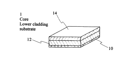
Fig. 1 is an isometric view of a two-layered planar structure on a flat
substrate serving as
a base for fabricating a waveguide device;
Fig. 2 is an isometric view of the device shown in Fig. 1 including a metal
mask disposed
atop an upper layer for use in providing grafted parts;
Fig. 3 is an isometric view of the device shown in Fig. 2 wherein three
grafting parts are
shown after removing unmasked material around the parts;
Fig. 4 is an isometric view of the device shown in Fig. 3 including an
additional spin
coated layer;
Fig. 5 is an isometric view of the device shown in Fig. 4 having a mask upon
the grafting
parts and adjacent polymer material for forming a longitudinal core section;
Fig. 6 is an isometric view of the device shown in Fig. 5, wherein the
composite core
3o with grafted sections are shown after removal of the unmasked surrounding
material,
awaiting a final upper cladding layer to be spin-coated thereon;
6
CA 02307248 2000-04-27
Doc. No 10-339 CA Patent
Fig. 7 is an isometric view of a waveguide device having a grafted core
surrounded by a
cladding;
Figs 8 through 11 are isometric views of a grafting process for providing
polymer core
sections into a silica core waveguide;
Figs. 12a through 12d illustrate different etch back states;
Fig. 13 is a cross sectional view from a prior art patent EP 0707113A1 in the
name of
Bosc et al assigned to France Telecom wherein a planar waveguide is disclosed
having
silica core and a polymer cladding region.
Fig. 14 is an isometric view of a hybrid core of an optical waveguide in
accordance with
to an embodiment of the invention;
Fig. 15 is an isometric view of an alternative hybrid core of an optical
waveguide;
Fig. 16 is a top view of an optical switch in accordance with a preferred
embodiment of
the invention; and,
Fig. 17 is a cross sectional view of the optical switch shown in Fig. 17 taken
along the
line a-a' in accordance with a preferred embodiment of the invention;
Detailed Description
The grafting of planar polymeric waveguides is known and is described in a
publication
2o entitled Novel "serially grafted" connection between functional and passive
polymer
waveguides, by Watanabe et al Appl. Phys. Lett. 65 (10), 5 Sept. 1994, pp.
1205-1207
The process steps required to create inlay-structures are shown in the figures
and begin
with spin-coating a lower cladding layer 12 onto a silicon substrate 10
followed by
coating the core polymer 14 as is shown in Fig. 1. This core layer is used to
create parts
to be grafted. Fig. 2 illustrates the application metal structures 16 used as
a mask for the
grafting parts and realized onto lift off resist by evaporation of a metal
layer, resist
spinning and definition~by photo-lithography. The grafting parts 18 are shown
in Fig. 3
after reactive ion etching (RIE) to remove the unmasked core layer material.
After a lift-
off step to remove the metal mask, a second core layer 20 is spin coated. The
remaining
3o portion of the waveguide core is formed by this layer. Conventional etch-
back
planarization is performed to reach a flat surface. A planarization layer is
spin-coated
7
CA 02307248 2000-04-27
Doc. No 10-339 CA Patent
onto the second core layer 20 and then etched back until the preferred
waveguide height
is reached. The topography of the upper surface of the planarization layer is
transferred
to the underlying layer. In this manner a polymer stack with grafted parts and
a flat
surface is reached as shown in Fig. 4. After this, another metal structure 22
is defined
onto lift-off resist, by evaporation of a metal layer, resist spinning and
definition by
photo-lithography with the final waveguide pattern as shown in Fig. 5. Fig. 6
illustrates
the waveguide consisting of grafted parts 18, 19 after reactive ion etching.
Fig. 7
illustrates the polymer stack after a final spin-coat 24 of upper cladding is
applied.
1 o Although optical devices made of two different polymer cores such as the
grafted cores
described heretofore are useful in certain optical applications, it is
believed that this
structure can greatly be improved upon.
This invention relates to the provision of an optical waveguide having a core
wherein a
15 region of the core is a polymer material and wherein an adjacent contiguous
region of of
the waveguide is inorganic glass preferably silica. Since silica is highly
transparent, and
less attenuating than polymer materials, it is preferable in most instances to
manufacture
devices wherein the core is substantially made of silica, and wherein a much
smaller
lesser portion is made of polymer. Furthermore, many of the benefits of
polymer can be
2o utilized by using only a small amount of polymer in these devices. For
example in an
active device such as an optical switch, the switching region itself can be
realized with a
small polymer grafted insert. In temperature stable devices, where the
advantageous
combination of combining a core of polymer with a core of silica is provided,
the ratio of
polymer to silica or glass is about 1:10, hence only a small amount of polymer
is required
25 in many instances in smaller devices. Polymer silica hybrid core waveguides
as
described hereafter are particularly suitable in optical switch or in-line
Bragg grating
applications for a plurality of reasons. Since a polymer silica core hybrid
waveguide can
be provided wherein the refractive index is the same at ambient temperature,
or at a
predetermined temperature, gratings can be manufactured which are
substantially
30 transmissive at a particular temperature and which are highly reflective at
other higher
temperatures for predetermined wavelengths of light. Hence such an optical
waveguide
CA 02307248 2000-04-27
Doc. No 10-339 CA Patent
would act as a reflective (or forward coupling) filter when heat is applied
and would act
as if the grating was absent when the heat was removed. Instead of the
multiple polymer
silica sections that are used in the gratings, a single polymer section would
act as a
wavelength insensitive reflector when heat is applied and would act as if the
reflector was
absent when the heat was removed.
Thus, practicable, useful active and passive optical devices can be made from
the
waveguides in accordance with this invention.
1o Figs. 1 through 7 as shown relate to the formation of a hybrid grafted core
section having
two different polymer materials adjacent one another forming the core of the
waveguide.
This process can be extended to yield a hybrid silica/polymer core in
accordance with this
invention. Referring now to Figs. 1 through 7 again, the initial base layers
12 and 14 are
now made of silica; these layers can be created by flame hydrolysis deposition
(FHD)
process or a chemical vapour deposition (CVD) process; these layers precede
polymer
layers because they fabricated at temperatures well above the degradation
temperature for
polymers. Initially the lower silica cladding layer 12 is deposited onto the
silicon
substrate 10, followed by the silica care layer 14. This is illustrated in
Fig. 1 Channel
waveguide core sections will be etched out of the core layer by means of
reactive ion
etching (RIE) in CHF3, Ar gas mixtures using a Cr mask. This mask 16 is
created by Cr
layer sputtering onto the core layer followed by standard photolithographic
resist
patterning and wet chemical etching. Hence openings for the polymer channels
section to
be disposed are provided as is illustrated in Fig. 2. After RIE, the mask is
removed by a
wet chemical etching process and the silica grafting parts 18 are ready for
polymer
overcoating as can be seen in Fig. 3 .
This is illustrated in Fig. 4 where a solution of cross-linkable polymer for
the core
sections has been spin-coated onto the wafer to embed the remaining silica
core sections
18 in the core polymer 20. Dependent on the polymer that is used, thermal or
photocuring
3o is used to make the polymer layer insoluble. Additional cured polymer
layers can be
deposited over this layer to further planarize the surface. The polymer
surface is then
9
CA 02307248 2000-04-27
Doc. No 10-339 CA Patent
etched down to the upper core surface using RIE with OZ. A continuous Ti mask
pattern
22 for the hybrid channel waveguide is formed onto this surface by means of a
standard
photolithographic resist patterning followed by dry etching using RIE with
SF~.This is
shown in Fig. 5 The Ti is evaporated onto a photoresist layer that is
spincoated first onto
the surface. Fig. 6 shows the continuous hybrid channel 18+19 that is created
by polymer
etching using OZ-RIE. The mask pattern is removed by a lift off procedure.
Finally a
polymer upper cladding layer 24 having a refractive index that is lower than
the refractive
index of the polymer core sections is spin-coated over the hybrid channel
waveguide
structure as illustrated in Fig. 7. After curing it forms an insoluble upper
cladding layer.
to The final waveguide is formed of core sections of silica 18 and adjacent
core sections 19
of polymer.
Fig. 8 to 11 show an alternative process that begins from silica channel
waveguides 34
including the upper silica cladding 32 (Fig. 8). Sections for the polymer core
are
provided by etching out the silica down to the lower silica cladding using a
metal mask
(Fig.9) to make grafting gaps in the silica core by RIE (Fig. 10). The gaps
are filled first
with the core polymer by spincoating and curing. This polymer is then etched
down by
RIE with 02 to the upper core interface. This process can be carried out
without the use
of a mask , because the silica is not etched in the RIE process for the
polymer. A
2o polymer cladding is applied thereafter (Fig. l l ).
Referring now to Figs 12a through 12d the etch back principle is illustrated.
To
successfully etch back the planarization material has to have the same etch
speed as the
core or grafting material. The initial situation is a layer stack which is
built up to the
planarization layer as show in 12a. When the etch rate of the planarization
material vp is
larger than the etch rate of the core materials v~ a bump will remain as
illustrated in Fig.
12b. When the etch rate of the planarization material is smaller than the etch
rate of the
core material a dent can arise as shown in Fig. 12c. Preferably as shown in
Fig. 12d, vp =
v~.
10
CA 02307248 2000-04-27
Doc. No 10-339 CA Patent
Fig. 13 shows in a prior art European patent application EP 0797113A1 in the
name of
Bosc et al. a planar waveguide having silica core and a polymer cladding
region.
Although there are advantages to such a structure, in contrast the instant
invention
provides a planar optical waveguide that provides an entirely new class of
optical
devices.
This invention provides control of and within the core of a waveguide itself.
Hence by using these two very compatible materials having significantly
different
1 o properties within a core of an optical waveguide, a host of new devices
are practicable;
devices which can route, switch, multiplex and modify channels or wavelengths
of light;
devices essential for optical communications. The core of the waveguide need
not be
confined to small dimension typically associated with single mode propagation
of light;
core dimensions may in fact be considerably larger, for example for use in
applications
such as multimode interference devices.
Referring now to Fig. 14, a core of an optical waveguide is shown, in
accordance with
this invention, having a polymer portion 12, grafted between two silica
sections 10. Of
course a suitable cladding is required (not shown) around the waveguide core
in Fig. 14
2o to ensure that light is confined within the core. Although the polymer
portion 12 and
silica sections 10 are adjacent and contiguous to one another in a
longitudinal sense,
serially one portion after the other, this invention is not confined to
longitudinal
contiguous sections or portions of silica and polymer within a core of a
waveguide. For
instance, in Fig. 15 a core is shown having two contiguous portions of silica
40 and
polymer 42, wherein there are no longitudinal abutting portions.
Mufti-mode interference couplers are well known and are described in the
following text:
L. B. Soldano and E. C. M. Pennings, Optical mufti-mode interference devices
based on
self imaging: principles and applications, J. Lightwave Technolgy. 13 (4), 615-
627
(1995).
CA 02307248 2000-04-27
Doc. No 10-339 CA Patent
Turning now to Fig. 16, an optical switch is shown having two optical
waveguides 176a
and 176b having input ends 172a 172b and output ends 174a and 174b. A cladding
layer
178 having a refractive index n~i, lower than the refractive index n~ of the
waveguide
cores is applied over the cores and over a mid-region. The mid-region is shown
as a
dotted rectangle and includes glass waveguides 176a and 176b as well as a thin
region of
a different material such as polymer 179. Since the switch is bi-directional,
input ends
may serve as output ends and output ends as input ends. When heat is applied
by a
heating element 180 in an active region defined by the dashed line indicating
the heating
element, the refractive index difference between the polymer and the glass
within the
to mid-region increases. Thus in the absence of heat, the refractive index of
the polymer is
the same as the refractive index of the glass and so that the refractive index
difference
between n~ and n2 is zero. It is preferred to have the mid-region as small as
possible while
maintaining the mode field of the cores. Thus, the horizontal second shown in
the mid-
region are made as small as possible. At the same time, it is preferred that
the waveguide
A be in line with the waveguide section B and that the waveguide section A' be
in line
with the waveguide section B'.
Total internal reflection ensures that light launched into end 172a will
propagate within
waveguide 176a and will continue along 176a until it reaches the output port
174a. For
2o this to occur, the polymer region 179 has to be of a refractive index n2,
wherein sin B ~ >_
n2/nl . Of course once the geometry of the X-pattern is established, switching
from one
path to another is accomplished by varying the refractive index difference
between the
polymer and the glass waveguide.
The circuit is preferably designed such that when no heat is applied, at
ambient
temperature, the polymer has the same refractive index as the waveguide core
and light
launched along A couples into B. In the presence of heat, light launched into
A remains
within the same waveguide and couples into B'. In this instance the refractive
index of
the polymer is less than that of glass and through total internal reflection
light remains in
waveguide 176a. In this mode light can be launched into both ends 172a and
172b
simultaneously and will be simultaneously be output at ends 174a and 174b
respectively.
12
CA 02307248 2000-04-27
Doc. No 10-339 CA Patent
Since the switch is a binary switch having a switched or unswitched state,
according to
Snell's law, when the conditions for total internal reflection apply the
switch will be in
one of two switching states, and when the conditions to not apply the switch
will be in the
other of the two switching states.
Of course the optical switch can be used as a two state modulator.
Fig. 17 shows a cross-section of the switch at the mid-region. A top cladding
is shown
1 o having a heating element over top and having an undercladding support
layer.
13