Note: Descriptions are shown in the official language in which they were submitted.
CA 02307340 2000-04-17
1
DESCRIPTION
ARRAYED WAVEGUIDE GRATING TYPE OPTICAL
MULTIPLEXER/DEMULTIPLEXER
Technical Field
The present invention relates to an arrayed waveguide
grating type optical multiplexer/demultiplexer used in
optical wavelength devision multiplexing communications,
and more particularly, to an arrayed waveguide grating type
optical multiplexer/demultiplexer of which the spectrum
response at output waveguides shows satisfactory flatness
in the vicinity of a center wavelength and which ensures
high yield during manufacture.
Background Art
Recently, in the field of optical communications,
researches have been intensively made on optical frequency
devision multiplexing communication techniques for
transmitting through a single optical fiber a plurality of
sets of information at different wavelengths of light, in
order to greatly increase the information transmission
capacity. To attain such multiplexing communications, an
optical multiplexer/demultiplexer is needed which
multiplexes and demultiplexes a large number of light waves
used.
The optical multiplexer/demultiplexer used for such
applications is required to have the performance stated
below.
First, using a large number of light waves with the
narrowest possible wavelength spacing is effective in
increasing the information transmission capacity, and
therefore, the optical multiplexer/demultiplexer should be
CA 02307340 2000-04-17
2
able to multiplex and demultiplex such a large number of
light waves. For example, the multiplexer/demultiplexer is
required to multiplex and demultiplex light waves with
100 GHz frequency spacing, which is equivalent
approximately to 0.8 nm wavelength spacing in 1.55 um band.
The optical multiplexer/demultiplexer is also required
to have satisfactory passband flatness in the vicinity of
passing wavelength.
For example, where an inexpensive LD is used as a
light source in constructing an optical frequency devision
multiplexing communication system with a view to reducing
costs, the oscillation wavelength of the light source is
liable to change with time or due to variations in
temperature or humidity of the environment in which the
light source is used. If the oscillation wavelength of the
light source undergoes such a change, a loss variation
occurs when light is propagated through the optical
multiplexer/demultiplexer in the system, by an amount
corresponding to the wavelength change depending on the
spectrum response of the multiplexer/demultiplexer. The
loss variation not only deteriorates the loss uniformity
among wavelengths to be multiplexed/demultiplexed but also
the S/N ratio, and eventually increases the cost of
constructing the system.
In view of the foregoing, the loss variation of the
optical multiplexer/demultiplexer should preferably be as
small as possible. The optical multiplexer/demultiplexer
is therefore required to have a characteristic such that
the loss variation is, for example, 1 dB or less, that is,
1 dB bandwidth is large.
As such optical multiplexer/demultiplexer, an arrayed
waveguide grating type is disclosed in Unexamined Japanese
Patent Publication (KOKAI) No. 8-122557.
CA 02307340 2000-04-17
3
FIG. 8 is a plan view schematically showing the
optical multiplexer/demultiplexer. This multiplexer/
demultiplexer has a substrate 1 on which are arranged one
or a plurality of input waveguides 2, an input-side slab
waveguide 3 connected to the input waveguide(s) 2, a
diffraction grating 4 connected to the input-side slab
waveguide 3 and comprising a plurality of arrayed channel
waveguides 4a, an output-side slab waveguide 5 connected to
the arrayed waveguide grating 4, and a plurality of output
waveguides 6 connected to the output-side slab waveguide 5.
In this optical multiplexer/demultiplexer, the
junction between the input waveguide 2 and the input-side
slab waveguide 3 is formed as shown in FIG. 9.
Specifically, the input waveguide 2, which is
surrounded by a cladding material 10 and has a path width
W1, has a tapered end portion expanded in the width
direction of the path, and a slit 7 is formed in the center
of the tapered portion, thus defining two waveguide
portions 2a and 2b of equal width. The input waveguide 2
is connected to the input-side slab waveguide 3 at the
tapered portion, or the two waveguide portions 2a and 2b.
In the input waveguide 2 constructed in this manner,
light propagated through the input waveguide 2 enters the
input-side slab waveguide via the tapered portion. At this
time, the two waveguide portions 2a and 2b of the tapered
portion equivalently function as a core. Consequently, at
a location just in front of the input-side slab waveguide 3,
the electric field distribution of light is spread as a
whole in the width direction and has a bimodal shape with
two maximal values.
This optical multiplexer/demultiplexer is allegedly
capable of attaining 3 dB bandwidth of about 0.8 nm with
respect to about 1 nm wavelength spacing.
CA 02307340 2000-04-17
4
In the prior art device, however, almost no
consideration is given to the passband flatness of light
output from the output waveguides 6, or more specifically,
to 1 dB bandwidth which is an important characteristic when
the optical multiplexer/demultiplexer is applied to an
actual optical frequency devision multiplexing
communication system.
The inventors hereof therefore actually fabricated an
optical multiplexer/demultiplexer as shown in FIGS. 8 and 9
and examined its spectrum response.
Specifically, an optical multiplexer/demultiplexer
with silica-based waveguides was produced, wherein the
input waveguide 2 had a path width W1 of 6.5 um, the
connecting portion of the input-side slab waveguide 3 had a
width W2 of 15.0 dam, the trapezoidal slit 7 had a
connection width CW of 1.0 pm on the input waveguide 2 side
and a connection width SW of 2.0 ~.un on the slab waveguide 3
side, the tapered portion was tapered at an angle 8 of 0.4°,
and the waveguides had a relative index difference of 0.8%
and a path height of 6.5 um, to derive light with 100 GHz
wavelength spacing, that is, about 0.8 nm wavelength
spacing in 1.55 um band. With light of 1.55 dun band input
to the input waveguide 2, the spectrum response was
examined.
FIG. 10 shows the electric field distribution of light
observed at a location just in front of the input-side slab
waveguide 3, and FIG. 11 shows the spectrum response at the
output waveguide 6.
In FIG. 10, the horizontal axis represents the width
direction of the path at a location immediately in front of
the input-side slab waveguide 3, and the position °0"
indicates the center along the width direction, that is,
the center point of the width W2 shown in FIG. 9. In FIG.
CA 02307340 2000-04-17
11, the horizontal axis represents wavelength of light
propagated through the output waveguide 6, and the position
"0" indicates the center wavelength of the propagated light.
To actually measure the electric field distribution,
5 the fabricated optical multiplexer/demultiplexer must be
destroyed, but in the experimentation, the electric field
distribution was estimated/calculated by means of
simulation according to beam propagation method (BPM),
instead of destroying the device.
As is clear from FIG. 10, the electric field
distribution showed a bimodal shape having maximal values a
and b and a minimal value c therebetween. The spacing
between the two maximal values a and b was 7.0 dun and the
ratio c/a was 0.59.
With regard to the spectrum response, 1 dB bandwidth,
which is a wavelength range 1 dB higher than a minimum
insertion loss, was found to be 0.37 nm, and 3 dB bandwidth
was 0.50 nm.
In the aforementioned Unexamined Japanese Patent
Publication No. 8-122557, it is stated that 3 dB bandwidth
can be further increased by setting the ratio SW/W2 of the
junction between the input waveguide and the input-side
slab waveguide shown in FIG. 9 to 0.2 to 0.6.
The inventors therefore fabricated an optical
multiplexer/demultiplexer with a junction having the same
parameters as the aforesaid ones, except that the
connection width SW of the junction shown in FIG. 9 was set
to 3.0 dun, and measured the electric field distribution and
the spectrum response under the same conditions. The
junction of the fabricated multiplexer/demultiplexer had an
SW/W2 ratio of 0.2.
FIG. 12 shows the electric field distribution of light
observed at a location just in front of the input-side slab
CA 02307340 2000-04-17
6
waveguide, and FIG. 13 shows the spectrum response of light
from the output waveguide.
In this device, the spacing between the maximal values
a and b shown in FIG. 12 was 10.3 um, which is greater than
the spacing (7.0 um) observed in the case of FIG. 10.
However, the ratio c/a was 0.27, showing an increased
difference between the maximal and minimal values in the
electric field distribution. Also, in the spectrum
response shown in FIG. 13, 3 dB bandwidth was 0.63 nm,
which is greater than the value (0.5 nm) observed in the
case of FIG. 11. However, the flatness of the output light
was so poor that the insertion loss at the center
wavelength was higher than the minimum loss by more than 1
dB, dividing 1 dB bandwidth into two with the center
wavelength missing. Namely, 1 dB bandwidth failed to be
widened.
The foregoing reveals the following.
(1) Where the electric field distribution of light at
a location immediately in front of the input-side slab
waveguide is made to have a bimodal shape with increased
spacing between the maximal values a and b, 3 dB bandwidth
of the spectrum response increases.
(2) If, in such a bimodal electric field distribution
of light at a location immediately in front of the input-
side slab waveguide, the difference between the maximal and
minimal values is large, the spectrum response of the
output waveguide shows increased insertion loss at the
center wavelength, with the result that 1 dB bandwidth
divides into two with no center wavelength.
The fact (2) poses a serious problem when the optical
multiplexer/demultiplexer is used in constructing an
optical frequency devision multiplexing communication
system, as mentioned above.
CA 02307340 2000-04-17
7
Thus, although the optical multiplexer/demultiplexer
disclosed in Unexamined Japanese Patent Publication No. 8-
122557 is effective in widening 3 dB passing bandwidth, it
is still associated with a problem that 1 dB bandwidth
fails to be widened satisfactorily.
Also, in this optical multiplexer/demultiplexer, the
slit structure formed at the junction between the input
waveguide and the input-side slab waveguide for
transforming an electric field distribution of the input
light into bimodal shape has a Y-branch configuration
constructed in closed space. It is therefore difficult to
form the slit structure with high precision, thus lowering
the yield during manufacture.
An object of the present invention is to provide an
arrayed waveguide grating type optical multiplexes/
demultiplexer which solves the aforementioned problems with
the optical multiplexer/demultiplexer disclosed in
Unexamined Japanese Patent Publication No. 8-122557 and
whose 3 dB and 1 dB bandwidths can both be widened,
compared with the prior art optical multiplexes/
demultiplexer. Another object of the present invention is
to provide an arrayed waveguide grating type optical
multiplexer/demultiplexer which ensures high yield during
manufacture, compared with the prior art optical
multiplexer/demultiplexer.
Disclosure of the Invention
To achieve the above objects, the present invention
provides an arrayed waveguide grating type optical
multiplexer/demultiplexer comprising: an input waveguide;
an input-side slab waveguide connected to an end portion of
the input waveguide; a diffraction grating including
arrayed channel waveguides connected to the input-side slab
CA 02307340 2000-04-17
8
waveguide; an output-side slab waveguide connected to the
arrayed waveguide diffraction grating; and output
waveguides having end portions connected to the output-side
slab waveguide, wherein a junction between the input
waveguide and the input-side slab waveguide or between each
output waveguide and the output-side slab waveguide is
tapered in a manner such that the end portion of the input
or output waveguide gradually widens in a width direction
of path toward the input-side or output-side slab waveguide,
and the junction includes two separate small-width
waveguide portions separate from the end portion of the
input or output waveguide and extending in a line with
taper of the tapered end portion, and a single large-width
waveguide portion separate from the small-width waveguide
portions.
The large-width waveguide portion constituting the
junction may be formed integrally with an input end portion
of the input-side slab waveguide or with an output end
portion of the output-side slab waveguide.
Alternatively, the large-width waveguide portion may
be arranged separately from the input end portion of the
input-side slab waveguide or from the output end portion of
the output-side slab waveguide.
The present invention also provides an arrayed
waveguide grating type optical multiplexer/demultiplexer
comprising: an input waveguide; an input-side slab
waveguide connected to an end portion of the input
waveguide; a diffraction grating including arrayed channel
waveguides connected to the input-side slab waveguide; an
output-side slab waveguide connected to the arrayed
waveguide diffraction grating; and output waveguides having
end portions connected to the output-side slab waveguide,
wherein a junction between the input waveguide and the
CA 02307340 2000-04-17
9
input-side slab waveguide or between each output waveguide
and the output-side slab waveguide is provided with input
means or output means for transforming an electric field
distribution of light into bimodal shape in a width
direction perpendicular to a propagation direction of light
at a location immediately in front of the input-side slab
waveguide or immediately behind the output-side slab
waveguide, and a connecting portion between the input means
and the input-side slab waveguide or between the output
means and the output-side slab waveguide is provided with a
waveguide for obtaining a bimodal electric field
distribution with a shallower central trough than that of
the first-mentioned bimodal electric field distribution.
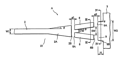
FIG. 1 is a schematic plan view showing an example of
an optical multiplexer/demultiplexer according to the
present invention, and FIG. 2 is a plan view showing
Example A of junction between an input waveguide and an
input-side slab waveguide.
In the optical multiplexer/demultiplexer according to
the present invention, waveguides formed on a substrate 1
are buried in a cladding material 10 with low refractive
index, the waveguides including one or a plurality of input
waveguides 2 having an end portions) connected to an
input-side slab waveguide 3, a diffraction grating 4
consisting of arrayed channel waveguides 4a connected to
the input-side slab waveguide 3, an output-side slab
waveguide 5 connected to the arrayed waveguide grating 4,
and a plurality of output waveguides 6 having end portions
connected to the output-side slab waveguide 5. This
structure is identical with that of the optical
multiplexer/demultiplexer of FIG. 8, disclosed in
Unexamined Japanese Patent Publication No. 8-122557.
The principal feature of the present invention is as
CA 02307340 2000-04-17
follows .
As shown in FIG. 2, the input waveguide 2 with a path
width W1 has a tapered end portion 2A which gradually
expands in the width direction of the path at an angle 8
5 with respect to an optical axis, and the tapered portion
has a distal end face 2B perpendicular to the optical axis.
Two separate small-width waveguide portions 8, 8 are
arranged near the end face 2B with a gap gl therebetween.
Specifically, as shown in FIG. 3 which is a sectional
10 view taken along line III-III in FIG. 2, the two small-
width waveguide portions 8, 8 are arranged in a manner
buried in the cladding material 10.
The small-width waveguide portions 8, 8 have
respective end faces 8A parallel to the end face 2B and
extend toward the input-side slab waveguide 3 at an angle 8
equal to the angle 8 at which the tapered end portion 2A of
the input waveguide is tapered. The small-width waveguide
portions 8, 8 have distal end faces 8B parallel to the end
faces 8A.
The input-side slab waveguide 3, which is located next
to the small-width waveguide portions 8, 8 in the direction
of propagation of light, has a large-width waveguide
portion 9 protruding therefrom toward the end faces 8B of
the small-width waveguide portions 8, 8 and having a
trapezoidal shape with a length H in plan view. The large-
width waveguide portion 9 serves as a connecting portion
for the small-width waveguide portions 8, 8.
The large-width waveguide portion 9 is formed as an
input end portion of the input-side slab waveguide such
that it is entirely buried in the cladding material 10, as
shown in FIG. 4 which is a sectional view taken along line
IV-IV in FIG. 2.
The large-width waveguide portion 9 has an end face 9A
CA 02307340 2000-04-17
11
separated from the end faces 8B of the small-width
waveguide portions 8, 8 with a gap g2 therebetween, and has
side faces 9B inclined at an angle equal to the
aforementioned taper angle 8.
Where the input waveguide 2 is one in number, it is
connected to the input-side slab waveguide by means of one
set of junction consisting of the two small-width waveguide
portions 8, 8 and the large-width waveguide portion 9. On
the other hand, where there are provided a plurality of
input waveguides 2, each of the input waveguides is
connected by means of such junction.
With the junction A constructed in this manner, the
optical power propagated through the input waveguide 2 is
spread in the width direction in the tapered portion 2A,
then propagated through the two small-width waveguide
portions 8, 8, and input to the large-width waveguide
portion 9 to be propagated through the input-side slab
waveguide 3.
At the junction A, the two small-width waveguide
portions 8, 8 are buried in the cladding material 10 with
low refractive index. Consequently, after passing through
the tapered portion 2A of the input waveguide 2 and the
small-width waveguide portions 8, 8, the light shows a
bimodal electric field distribution having a deep trough in
a central portion c thereof, as shown in FIG. 5, at a
location immediately behind the small-width waveguide
portions 8, 8.
Also, the junction A has the gaps gl and g2
respectively between the end portion 2A of the input
waveguide and each small-width waveguide portion 8 and
between each small-width waveguide portion 8 and the large-
width waveguide portion 9. Accordingly, the light
confinement effect is lost at each of these gaps, producing
CA 02307340 2000-04-17
12
a light diffraction effect, and thus the light comes to
have a bimodal electric field distribution having a
slightly shallower trough with the minimal value c
relatively increased, and falls upon the large-width
waveguide portion 9 to be propagated therethrough. Namely,
the large-width waveguide portion 9 serves as a connecting
portion for connecting the input waveguide 2 to the input-
side slab waveguide 3 or a connecting portion for
connecting the output-side slab waveguide 5 to the output
waveguide 6.
The large-width waveguide portion 9, which is a high
refractive index layer, functions as a three-dimensional
waveguide and the light having the aforementioned minimal
value c in its electric field distribution is propagated
through this waveguide portion 9. Consequently, as the
light having the bimodal electric field distribution with a
deep center trough as shown in FIG. 5 is propagated through
the large-width waveguide portion 9, the minimal value c at
the center trough relatively increases and the light
eventually comes to have an electric field distribution
with a reduced difference between its maximal and minimal
values, as shown in FIG. 6, at a location just in front of
the input-side slab waveguide 3. The spectrum response at
the output waveguide therefore shows satisfactory flatness
in the vicinity of the center wavelength.
Since the junction A is provided with the gaps gl and
g2, variations in shape of the individual waveguides can be
lessened when the waveguides are formed by etching, and
thus high yield can be attained compared with the case of
forming slits during the manufacture of the conventional
optical multiplexer/demultiplexer shown in FIG. 9.
As described above, in the optical multiplexer/
demultiplexer according to the present invention, the
CA 02307340 2000-04-17
13
junction between the input waveguide and the input-side
slab waveguide is provided with input means, or the small-
width waveguide portions, for transforming the electric
field distribution of light into bimodal shape, and also
with the large-width waveguide portion for shallowing the
center trough in the bimodal electric field distribution,
whereby the spectrum response at the output waveguide can
be flattened in the vicinity of the center wavelength.
FIG. 7 illustrates another junction B according to the
present invention.
As distinct from the junction A described above, the
junction B has a structure wherein the large-width
waveguide portion 9 is separated at a distance of a gap g3
from an input end portion 3a of the input-side slab
waveguide 3. Also with this structure, the difference
between maximal and minimal values of the bimodal electric
field distribution of light is reduced at a location
immediately in front of the input-side slab waveguide 3,
whereby the flatness of pass band improves.
The foregoing description is given with reference to
the case where the aforementioned junction is provided
between the input waveguide and the input-side slab
waveguide, but also in the case where the junction is
provided between the output-side slab waveguide and the
output waveguide, the optical multiplexer/demultiplexer of
the present invention can perform a similar function.
Brief Description of the Drawings
FIG. 1 is a schematic plan view of an optical
multiplexer/demultiplexer according to the present
invention;
FIG. 2 is a plan view showing a junction A of the
optical multiplexer/demultiplexer according to the present
CA 02307340 2000-04-17
14
invention;
FIG. 3 is a sectional view taken along line III-III in
FIG. 2;
FIG. 4 is a sectional view taken along line IV-IV in
FIG. 2;
FIG. 5 is a graph showing an electric field
distribution of light at a location just in front of a
large-width waveguide portion of the optical multiplexes/
demultiplexer according to the present invention;
FIG. 6 is a graph showing an electric field
distribution of light at a location just in front of an
input-side slab waveguide of the optical multiplexes/
demultiplexer according to the present invention;
FIG. 7 is a plan view showing another junction B of an
optical multiplexer/demultiplexer according to the present
invention;
FIG. 8 is a schematic plan view of a conventional
optical multiplexer/demultiplexer;
FIG. 9 is a plan view showing a connecting portion of
the optical multiplexer/demultiplexer shown in FIG. 8;
FIG. 10 is a graph showing an electric field
distribution of light at a location just in front of an
input-side slab waveguide;
FIG. 11 is a graph showing a spectrum response at an
output waveguide;
FIG. 12 is a graph showing another electric field
distribution of light at a location just in front of the
input-side slab waveguide; and
FIG. 13 is a graph showing another spectrum response
at the output waveguide.
Best Mode of Carrying out the Invention
Example 1
CA 02307340 2000-04-17
An optical multiplexer/demultiplexer as shown in FIGS.
1 and 2 was fabricated on an Si substrate by using a
combination of flame hydrolysis deposition,
photolithography and etching such that 100 GHz wavelength
5 spacing, that is, about 0.8 nm wavelength spacing in 1.55
um band, was obtained.
Specifically, a lower cladding layer (main component:
Si02) and a core layer (Si02 as a main component admixed
with Ti) were successively formed by flame hydrolysis
10 deposition on the Si substrate, and the entire structure
was heated so as to change into transparent glass.
Subsequently, the core layer was dry-etched using a
photomask, and after an upper cladding layer (main
component: Si02) was formed by flame hydrolysis deposition
15 such that the dry-etched core layer was buried therein, the
structure was heated so as to change the upper cladding
layer into transparent glass, thereby obtaining an optical
multiplexer/demultiplexer.
The optical multiplexer/demultiplexer had a junction A
configured as stated below.
The input waveguide 2 had a path width W1 of 6.5 pm,
and the large-width waveguide portion 9 had a width W2 of
15.0 pm and a protrusion length H of 30 um. The taper
angle 8 of the individual elements was 0.4°, a distance CW
between the end faces 8A of the small-width waveguide
portions was 3.0 um, a distance SW between the end faces 8B
of the same waveguide portions was 3.5 ucn, and the gaps gl
and g2 were both 5.0 dun. The individual waveguides had a
relative index difference of 0.8~ and a path height of
6.5 pm.
With light of 1.55 pm wavelength band input to the
input waveguide 2, the spectrum response was examined.
First, the electric field distribution of light at a
CA 02307340 2000-04-17
16
location immediately in front of the input-side slab
waveguide 3 was observed by means of simulation according
to beam propagation method, and it had a bimodal shape
identical with that shown in FIG. 6. The spacing between
the maximal values a and b was 11.7 dam and the ratio c/a
was 0.64, showing a shallow trough at the minimal value.
The spectrum response at the output waveguide showed a
small loss in the vicinity of the center wavelength and was
flat as a whole. The 3 dB bandwidth was 0.59 nm and the 1
dB bandwidth was 0.47 nm.
Example 2
An optical multiplexer/demultiplexer was produced
which had a junction B whose gap g3 was 5 um and whose
other parameters were identical with those of the
aforementioned junction A.
With regard to this optical multiplexer/demultiplexer,
the electric field distribution of light just in front of
the input-side slab waveguide and the spectrum response
were examined in the same manner as in Example 1.
In the observed electric field distribution of light,
the spacing between the maximal values a and b was 11.8 pm
and the ratio c/a was 0.63. The 3 dB bandwidth was 0.60 nm
and the 1 dB bandwidth was 0.48 nm.
Industrial Applicability
In the arrayed waveguide grating type optical
multiplexer/demultiplexer according to the present
invention, the electric field distribution of light shows a
bimodal shape at a location immediately in front of the
input-side slab waveguide and yet the difference between
the maximal and minimal values is small, so that the
spectrum response has satisfactory flatness. As a
consequence, both the 3 dB bandwidth and the 1 dB bandwidth
CA 02307340 2000-04-17
17
can be made wider than in the case of the conventional
arrayed waveguide grating type optical multiplexer/
demultiplexer.
Accordingly, the optical multiplexer/demultiplexer has
high industrial value as a component to be used in
constructing an optical frequency devision multiplexing
communication system.